


 Программирование
Похожие презентации:


")
Overview
1.
Overview2.
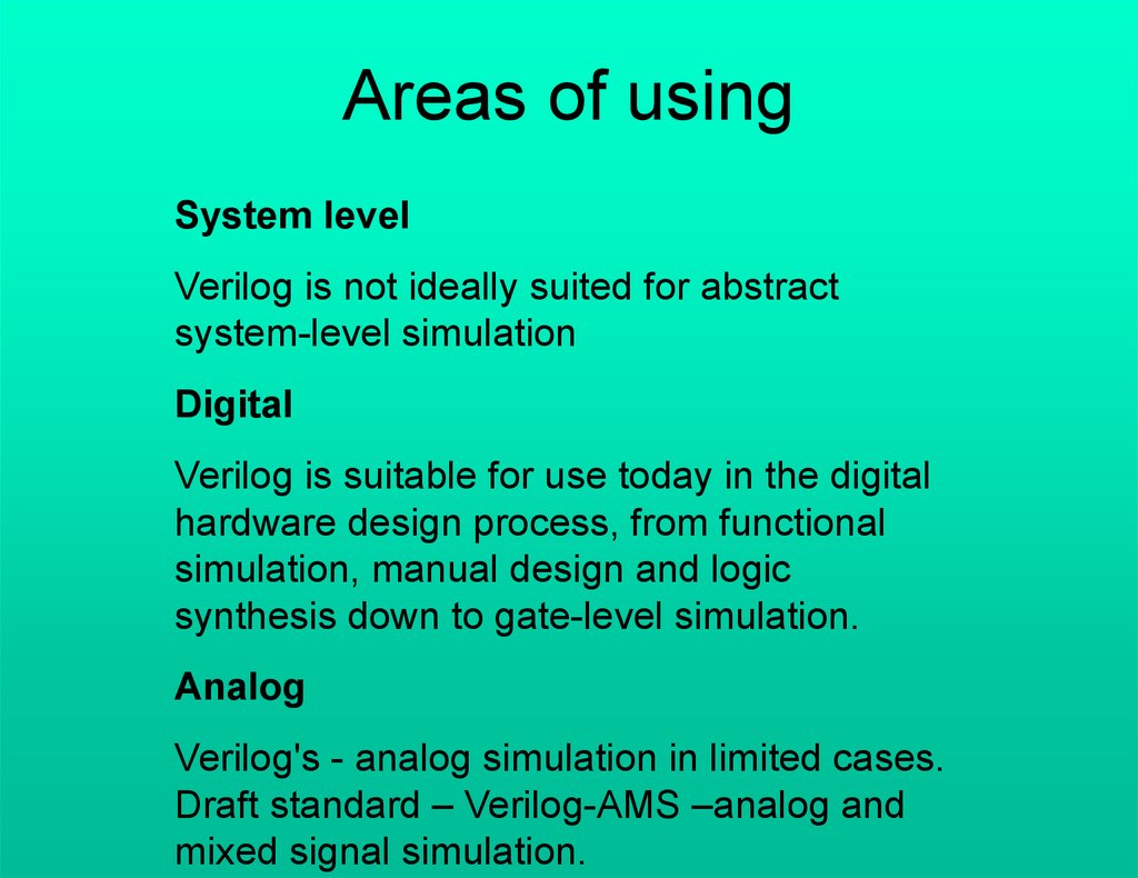
Areas of usingSystem level
Verilog is not ideally suited for abstract
system-level simulation
Digital
Verilog is suitable for use today in the digital
hardware design process, from functional
simulation, manual design and logic
synthesis down to gate-level simulation.
Analog
Verilog's - analog simulation in limited cases.
Draft standard – Verilog-AMS –analog and
mixed signal simulation.
3.
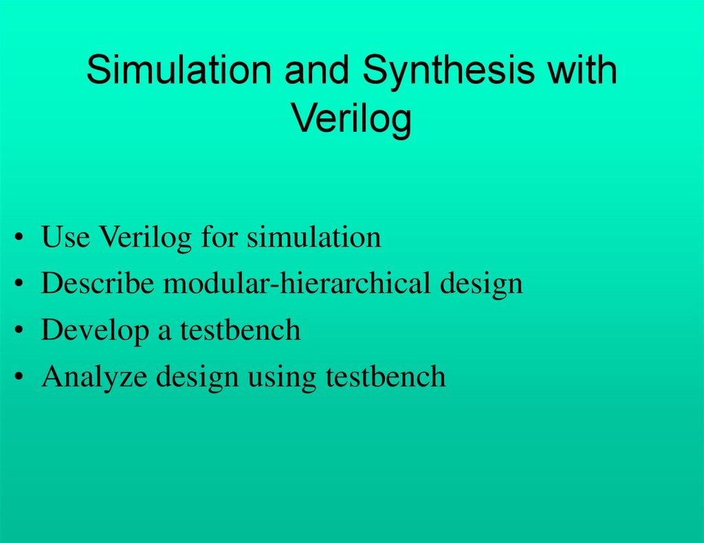
Simulation and Synthesis withVerilog
Use Verilog for simulation
Describe modular-hierarchical design
Develop a testbench
Analyze design using testbench
4.
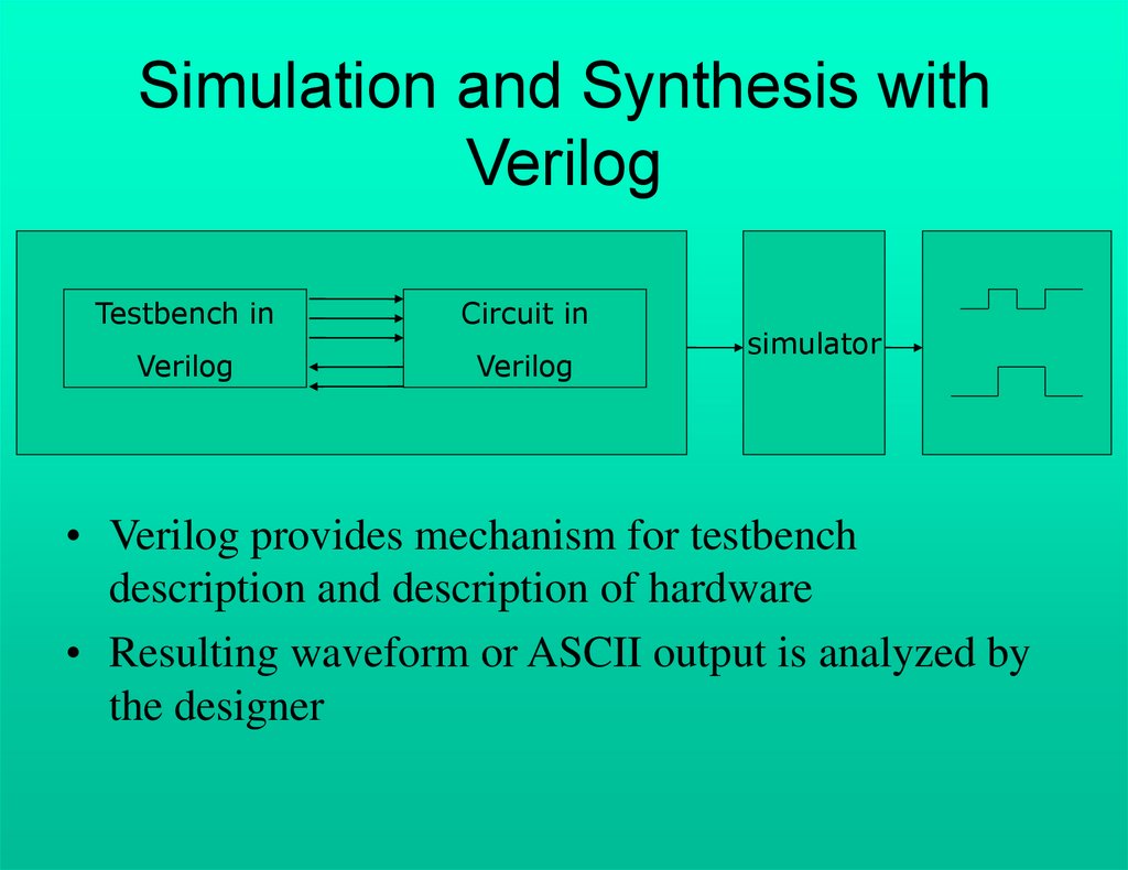
Simulation and Synthesis withVerilog
Testbench in
Circuit in
Verilog
Verilog
simulator
• Verilog provides mechanism for testbench
description and description of hardware
• Resulting waveform or ASCII output is analyzed by
the designer
5.
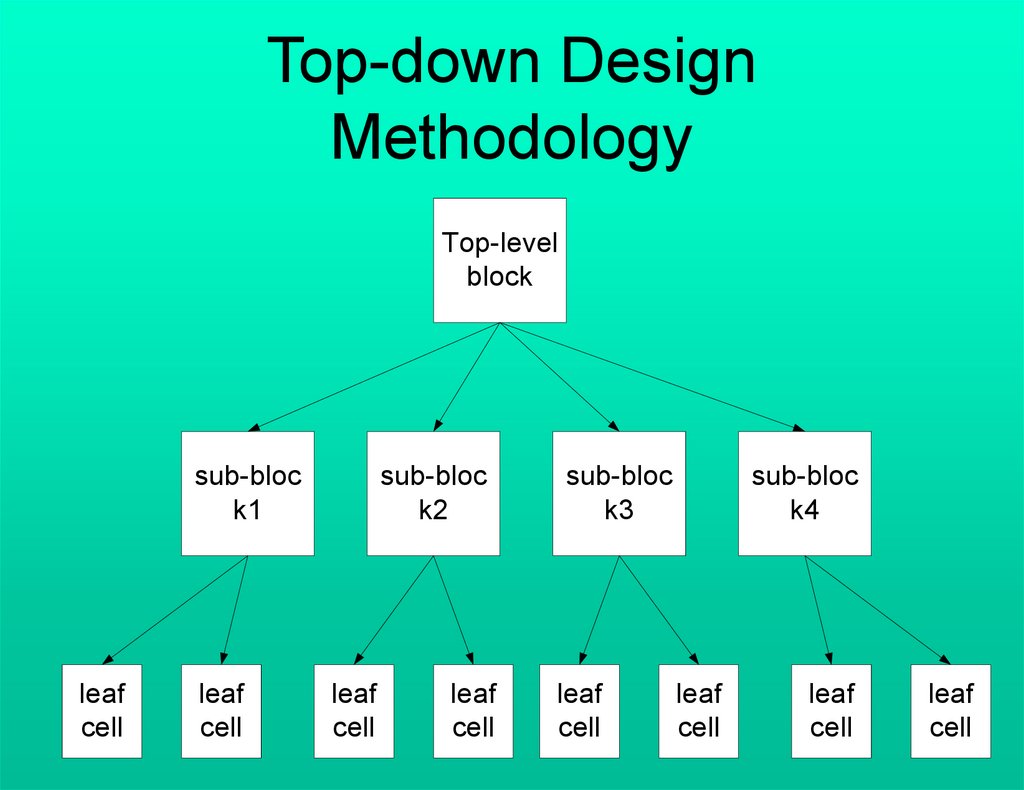
Top-down DesignMethodology
Top-level
block
sub-bloc
k1
leaf
cell
leaf
cell
sub-bloc
k2
leaf
cell
leaf
cell
sub-bloc
k3
leaf
cell
sub-bloc
k4
leaf
cell
leaf
cell
leaf
cell
6.
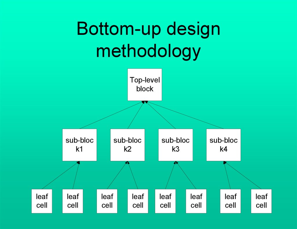
Bottom-up designmethodology
Top-level
block
sub-bloc
k1
leaf
cell
leaf
cell
sub-bloc
k2
leaf
cell
leaf
cell
sub-bloc
k3
leaf
cell
sub-bloc
k4
leaf
cell
leaf
cell
leaf
cell
7.
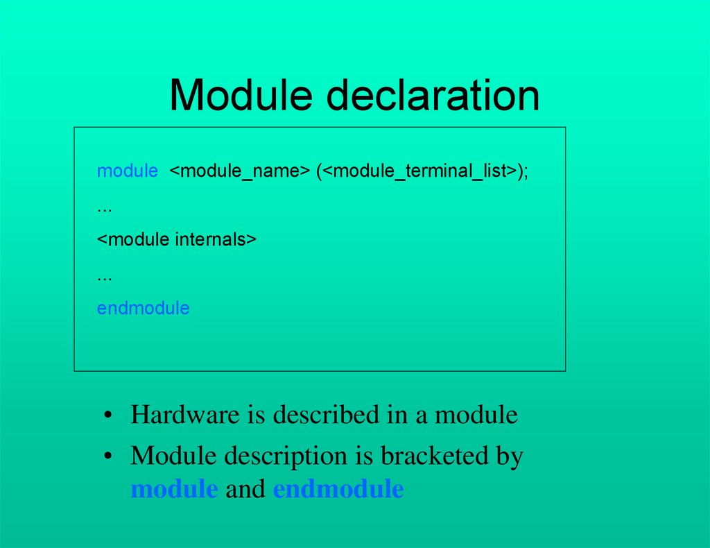
Module declarationmodule <module_name> (<module_terminal_list>);
...
<module internals>
...
endmodule
• Hardware is described in a module
• Module description is bracketed by
module and endmodule
8.
Module examplemodule T_FF (q, clock, reset);
.
.
<functionality of T-flipflop>
.
.
endmodule
9.
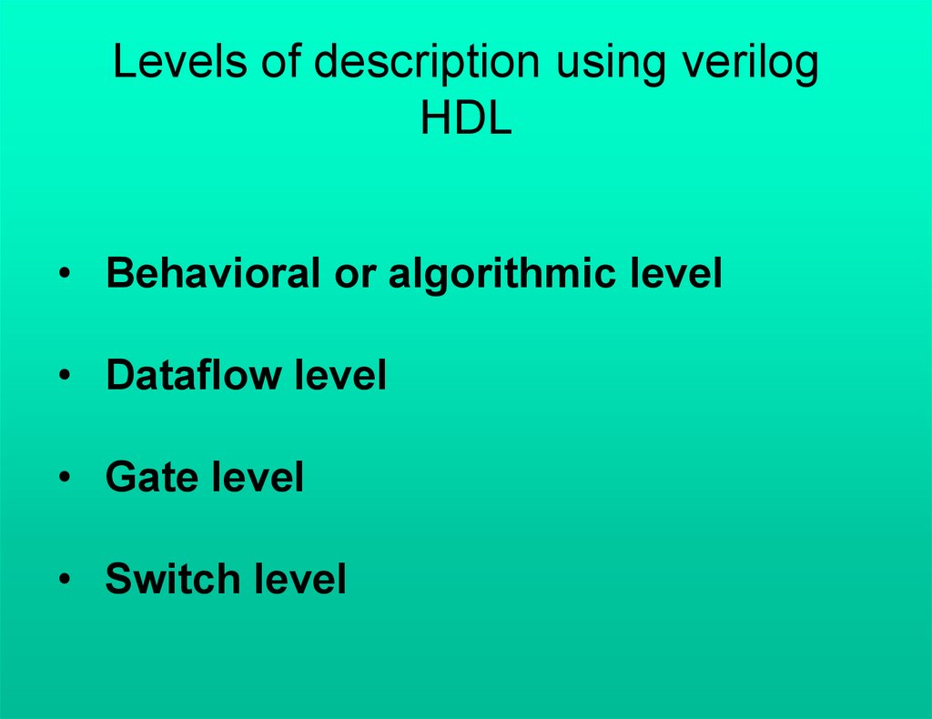
Levels of description using verilogHDL
• Behavioral or algorithmic level
• Dataflow level
• Gate level
• Switch level
10.
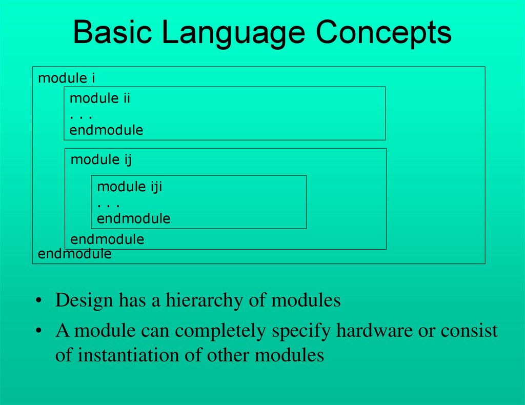
Basic Language Conceptsmodule i
module ii
...
endmodule
module ij
module iji
...
endmodule
endmodule
endmodule
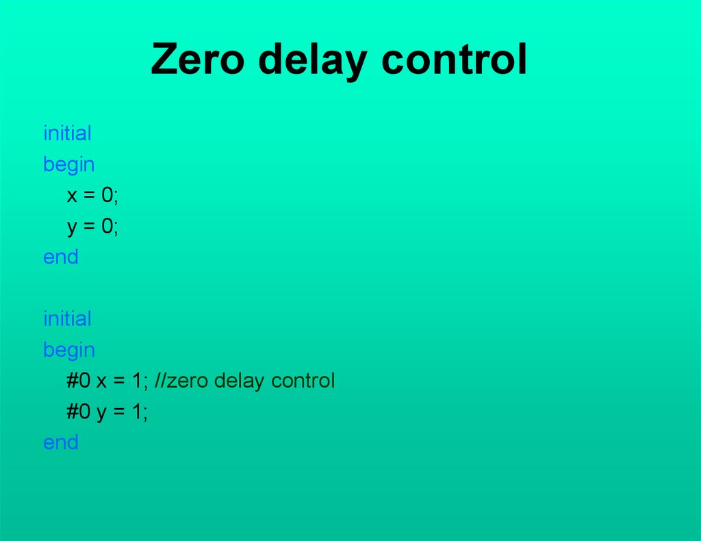
• Design has a hierarchy of modules
• A module can completely specify hardware or consist
of instantiation of other modules
11.
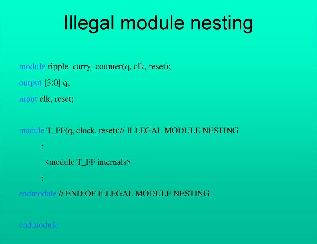
Illegal module nestingmodule ripple_carry_counter(q, clk, reset);
output [3:0] q;
input clk, reset;
module T_FF(q, clock, reset);// ILLEGAL MODULE NESTING
:
<module T_FF internals>
:
endmodule // END OF ILLEGAL MODULE NESTING
endmodule
12.
Instancesmodule i
module ii
...
endmodule
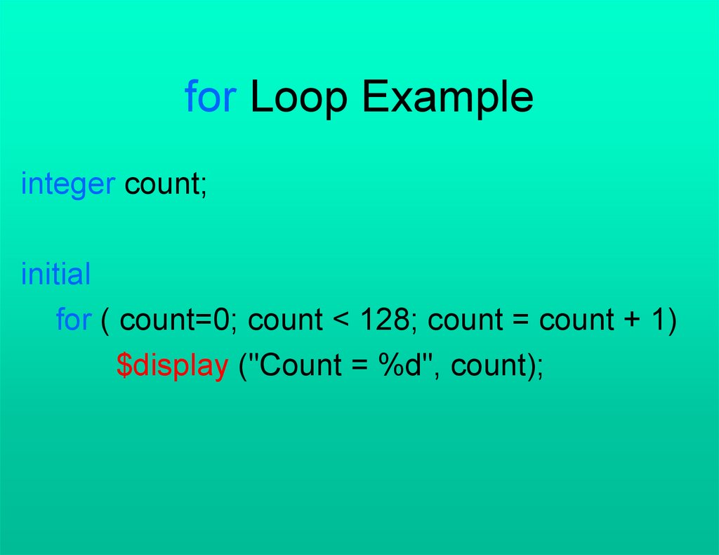
module ij
module iji
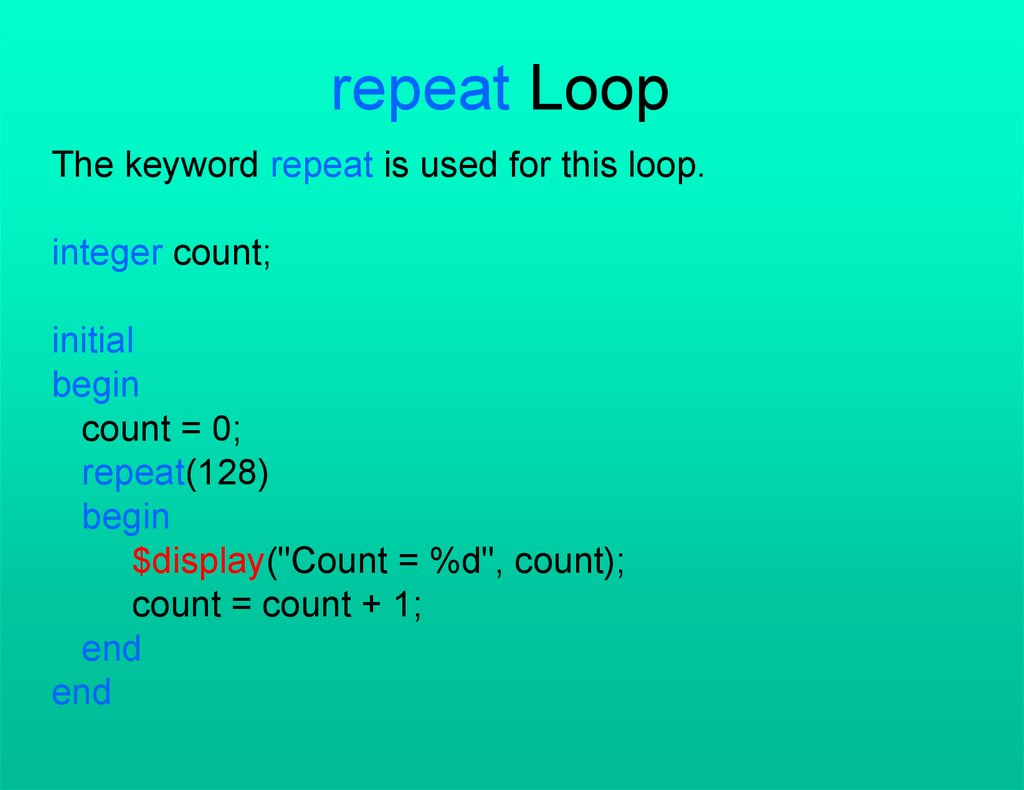
...
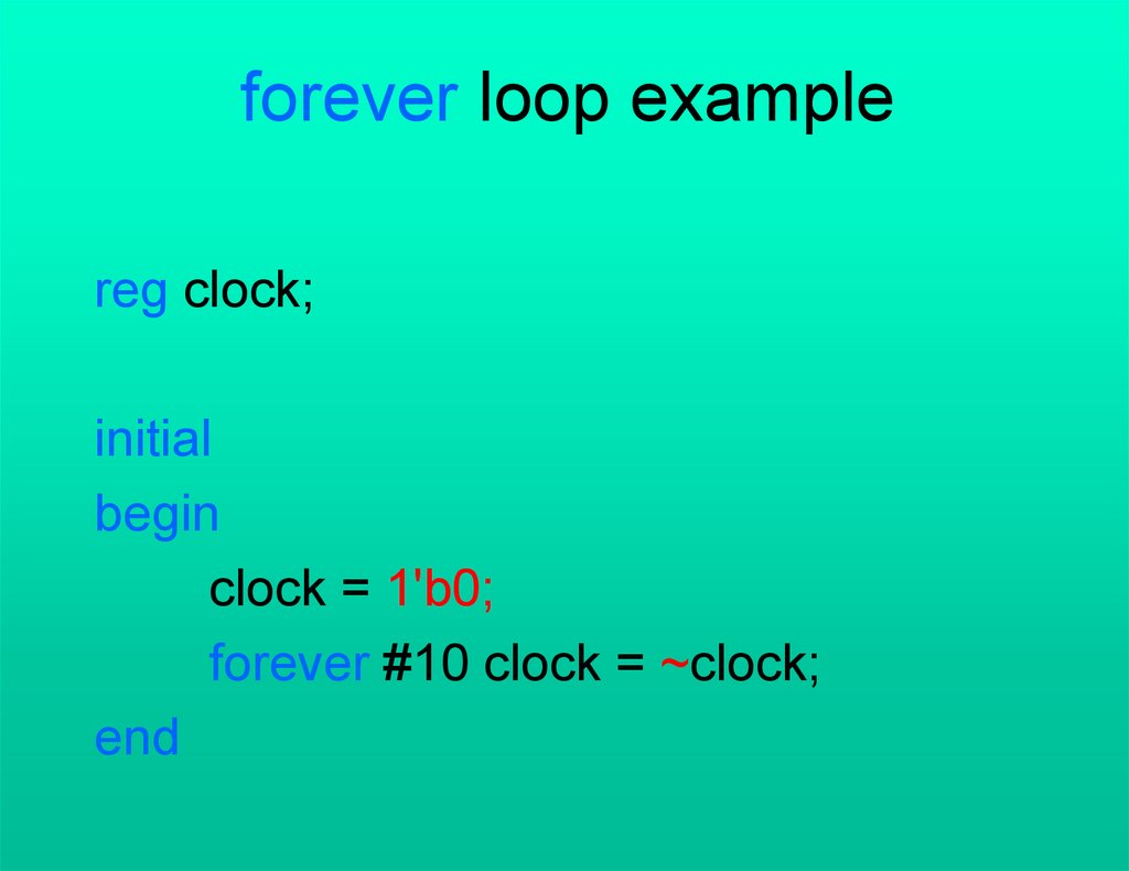
endmodule
endmodule
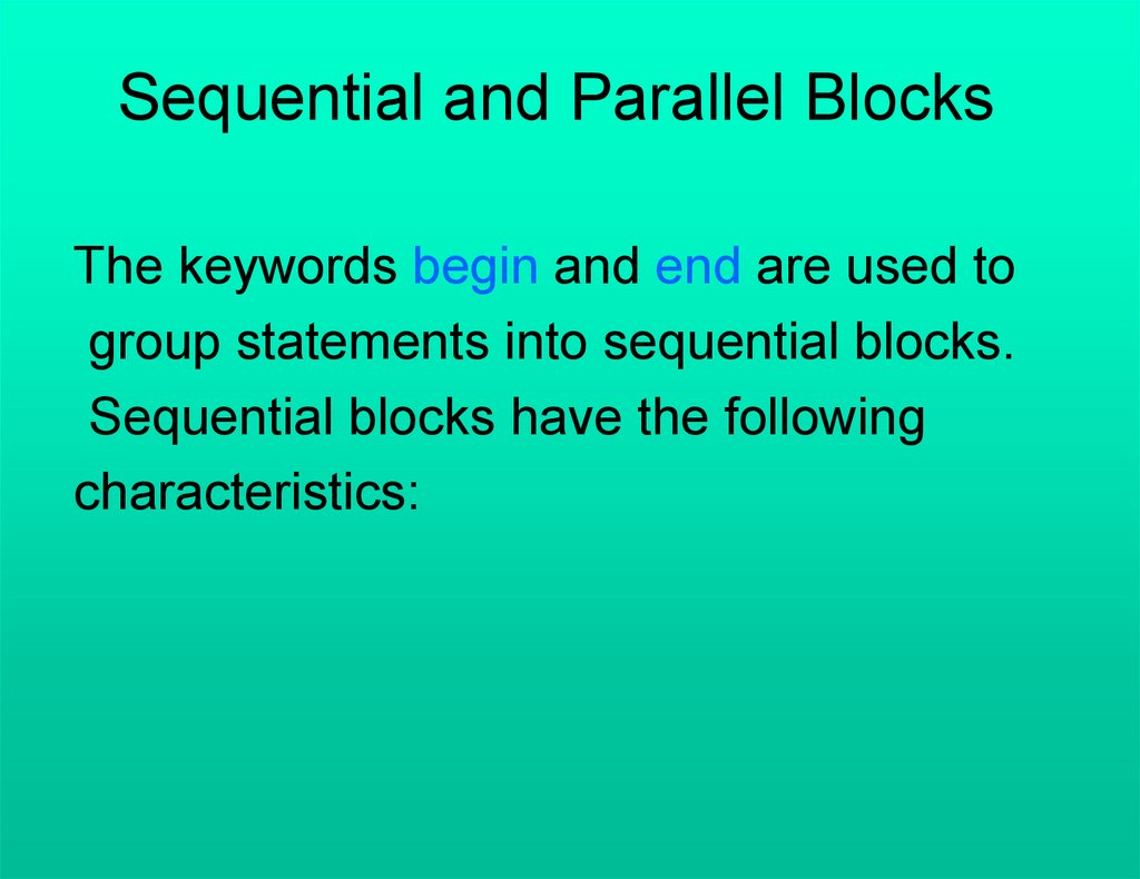
endmodule
• Design has a hierarchy of modules
• A module can completely specify hardware or consist
of instantiation of other modules
13.
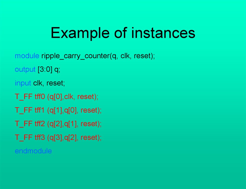
Example of instancesmodule ripple_carry_counter(q, clk, reset);
output [3:0] q;
input clk, reset;
T_FF tff0 (q[0],clk, reset);
T_FF tff1 (q[1],q[0], reset);
T_FF tff2 (q[2],q[1], reset);
T_FF tff3 (q[3],q[2], reset);
endmodule
14.
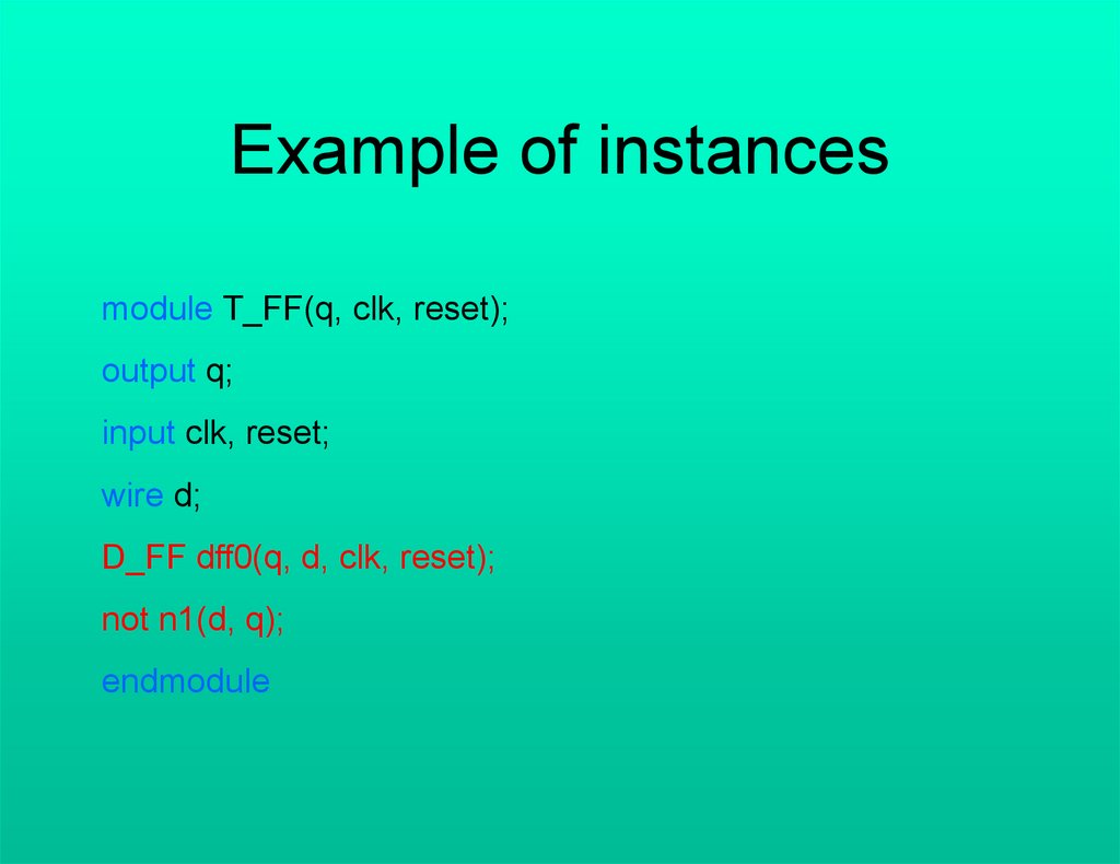
Example of instancesmodule T_FF(q, clk, reset);
output q;
input clk, reset;
wire d;
D_FF dff0(q, d, clk, reset);
not n1(d, q);
endmodule
15.
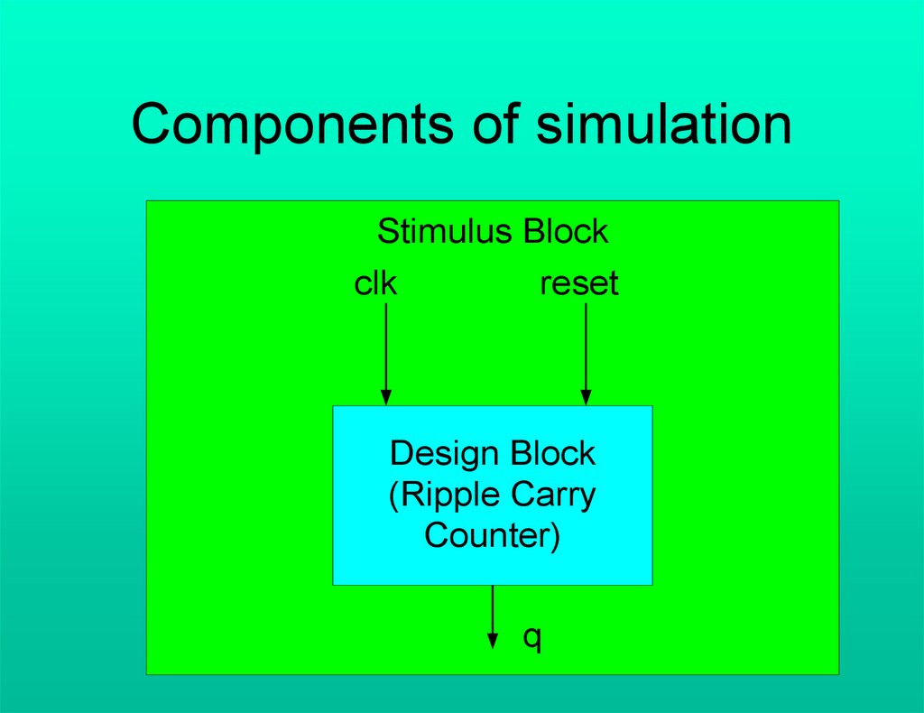
Components of simulationStimulus Block
clk
reset
Design Block
(Ripple Carry
Counter)
q
16.
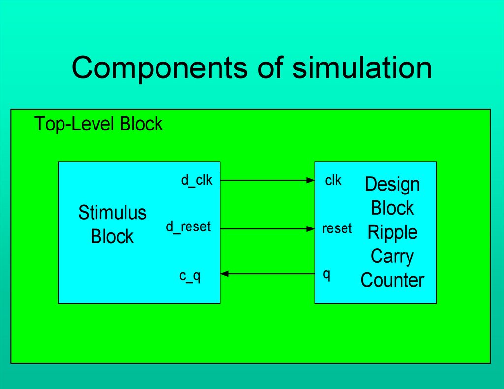
Components of simulationTop-Level Block
d_clk
Stimulus
Block
d_reset
c_q
clk
reset
q
Design
Block
Ripple
Carry
Counter
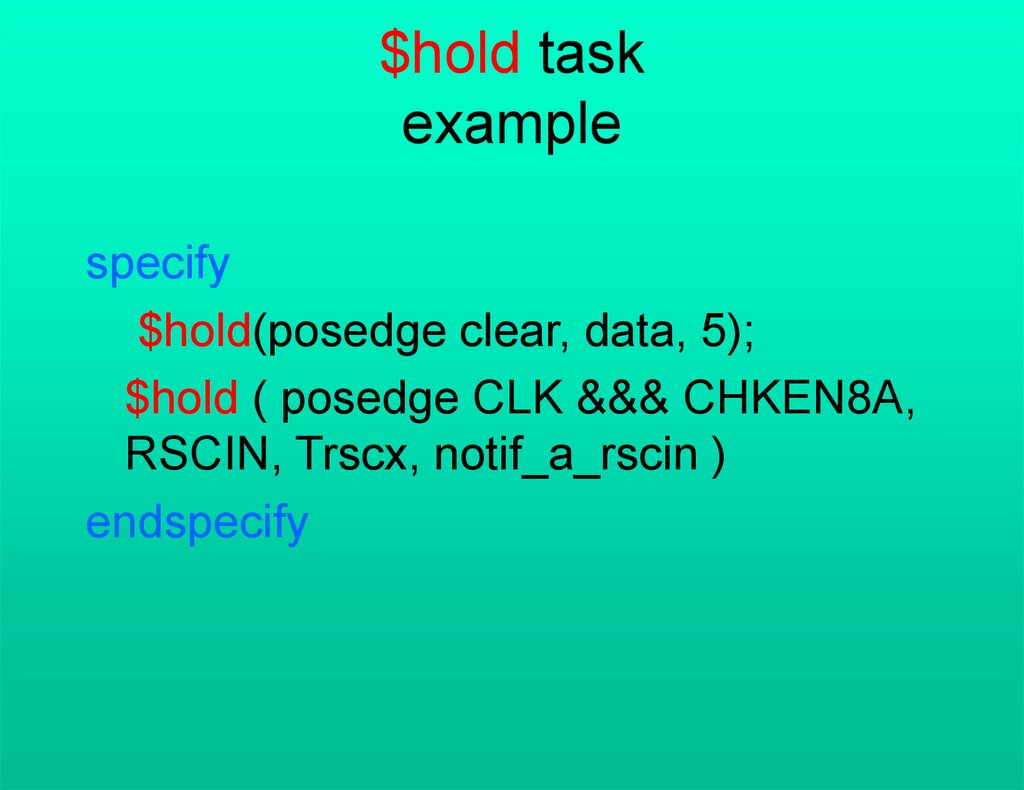
17.
Summary•Two kinds of design methodologies are used for digital
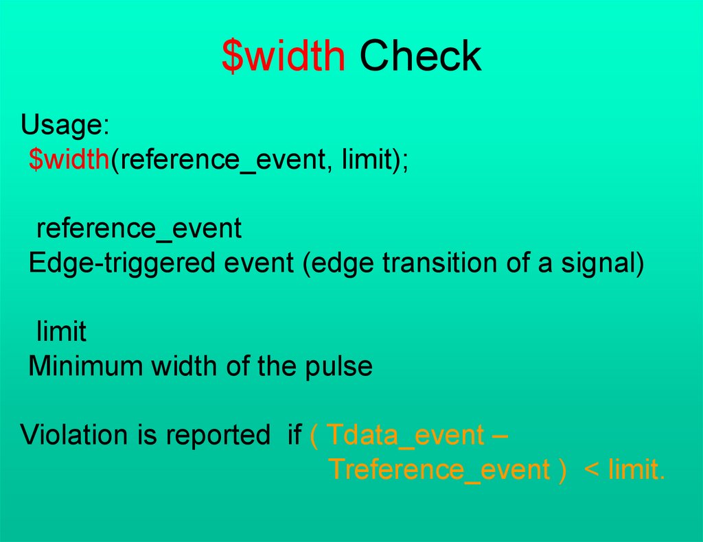
design: top-down and bottom-up
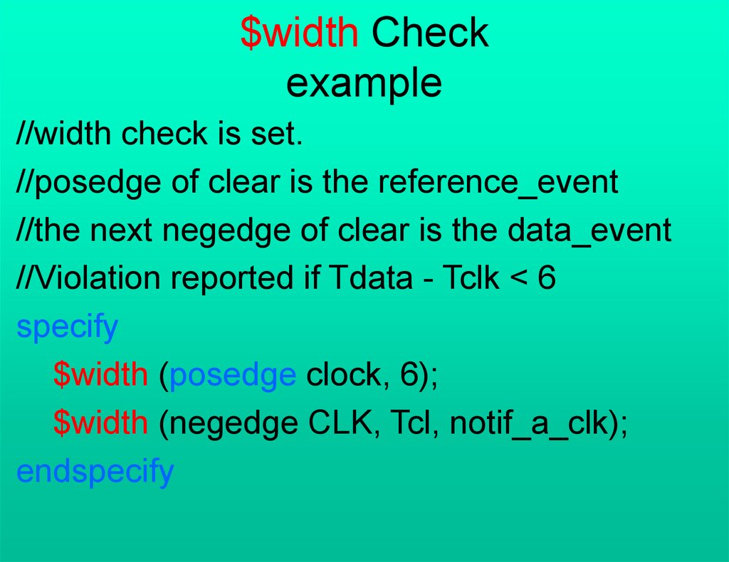
•Modules are the basic building blocks in Verilog.
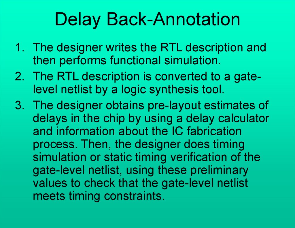
Modules are used in a design by instantiation. An
instance of a module has a unique identity and is different
from other instances of the same module. Each instance
has an independent copy of the internals of the module.
•There are two distinct components in a simulation: a
design block and a stimulus block. A stimulus block is
used to test the design block. The stimulus block is
usually the top-level block. There are two different styles
of applying stimulus to a design block.
18.
Lexical ConventionsComments
A one-line comment - //
A multiple-line comment or block
comment "/*" and ends with "*/".
a = b && c; // This is a one-line comment
/* This is a multiple line comment */
19.
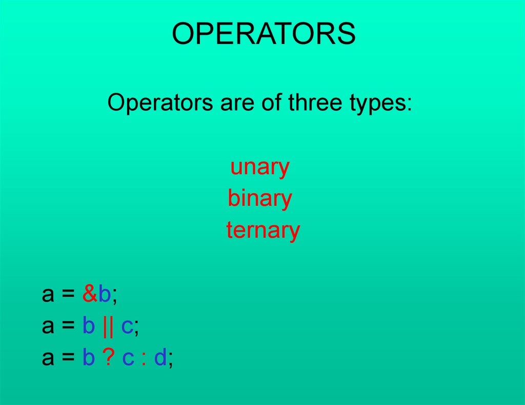
OPERATORSOperators are of three types:
unary
binary
ternary
a = &b;
a = b || c;
a = b ? c : d;
20.
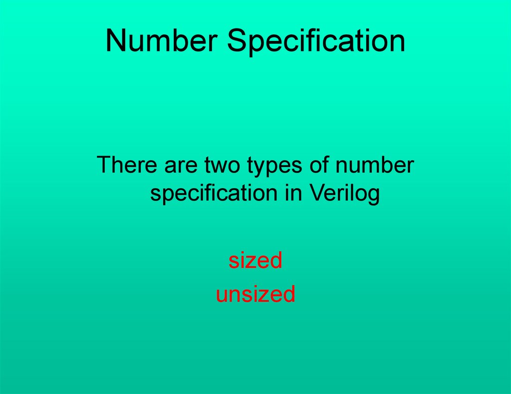
Number SpecificationThere are two types of number
specification in Verilog
sized
unsized
21.
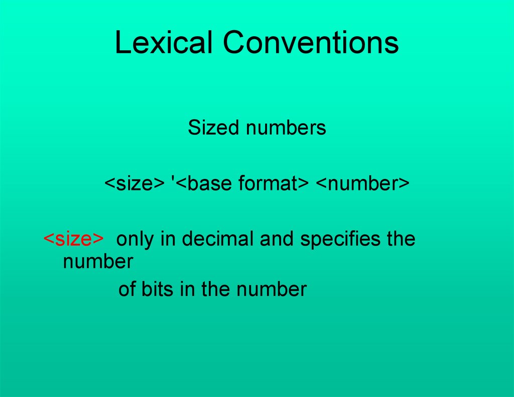
Lexical ConventionsSized numbers
<size> '<base format> <number>
<size> only in decimal and specifies the
number
of bits in the number
22.
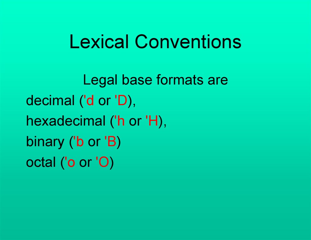
Lexical ConventionsLegal base formats are
decimal ('d or 'D),
hexadecimal ('h or 'H),
binary ('b or 'B)
octal ('o or 'O)
23.
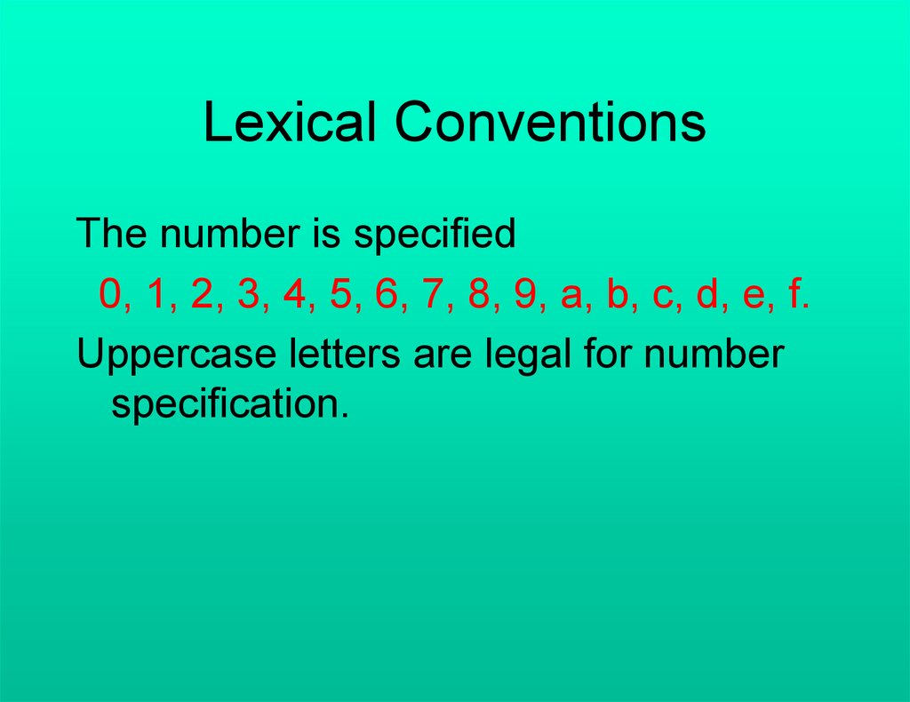
Lexical ConventionsThe number is specified
0, 1, 2, 3, 4, 5, 6, 7, 8, 9, a, b, c, d, e, f.
Uppercase letters are legal for number
specification.
24.
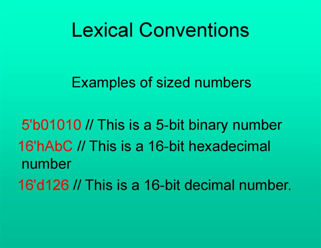
Lexical ConventionsExamples of sized numbers
5'b01010 // This is a 5-bit binary number
16'hAbC // This is a 16-bit hexadecimal
number
16'd126 // This is a 16-bit decimal number.
25.
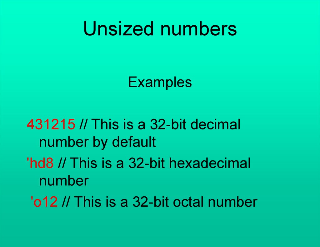
Unsized numbersExamples
431215 // This is a 32-bit decimal
number by default
'hd8 // This is a 32-bit hexadecimal
number
'o12 // This is a 32-bit octal number
26.
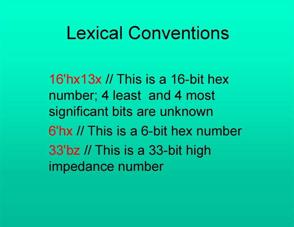
Lexical Conventions16'hx13x // This is a 16-bit hex
number; 4 least and 4 most
significant bits are unknown
6'hx // This is a 6-bit hex number
33'bz // This is a 33-bit high
impedance number
27.
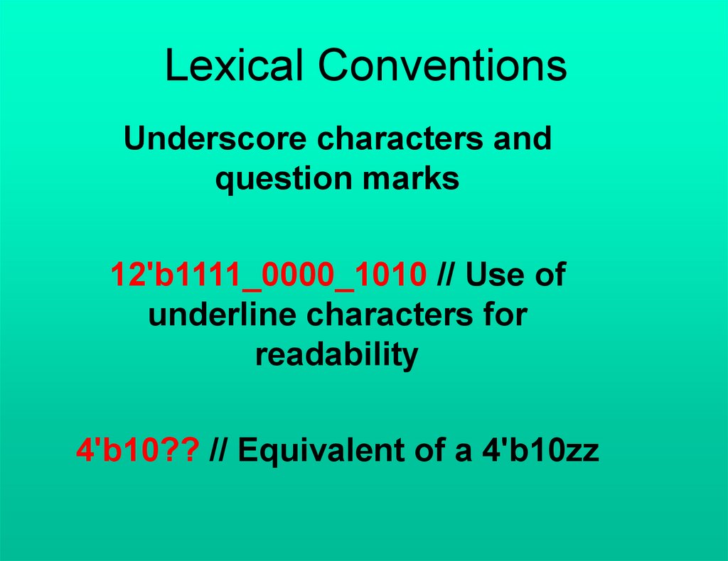
Lexical ConventionsUnderscore characters and
question marks
12'b1111_0000_1010 // Use of
underline characters for
readability
4'b10?? // Equivalent of a 4'b10zz
28.
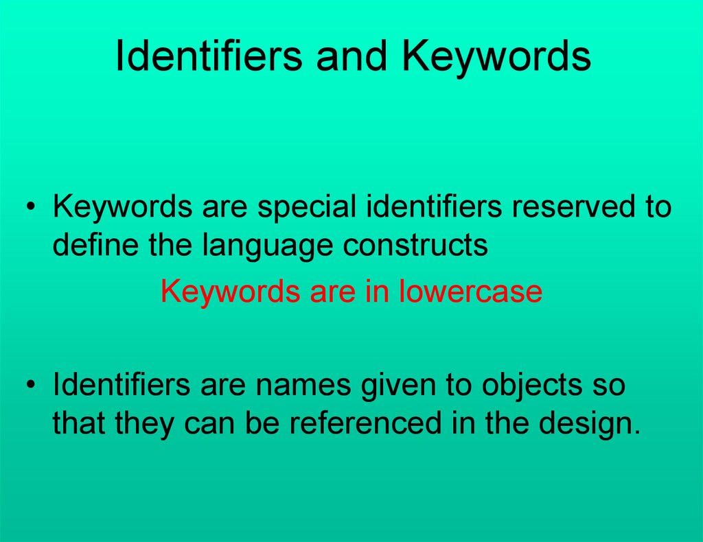
Identifiers and Keywords• Keywords are special identifiers reserved to
define the language constructs
Keywords are in lowercase
• Identifiers are names given to objects so
that they can be referenced in the design.
29.
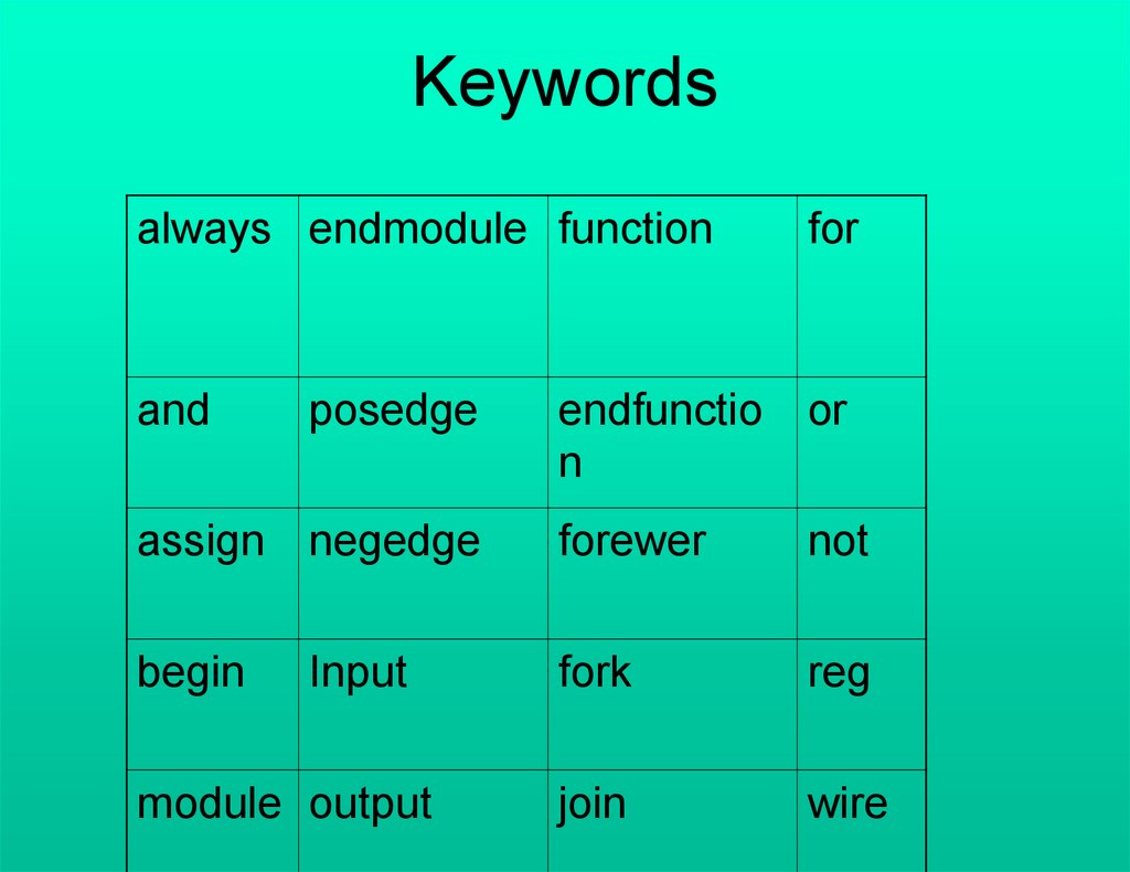
Keywordsalways endmodule function
for
and
endfunctio
n
or
assign negedge
forewer
not
begin
fork
reg
join
wire
posedge
Input
module output
30.
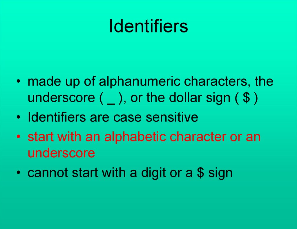
Identifiers• made up of alphanumeric characters, the
underscore ( _ ), or the dollar sign ( $ )
• Identifiers are case sensitive
• start with an alphabetic character or an
underscore
• cannot start with a digit or a $ sign
31.
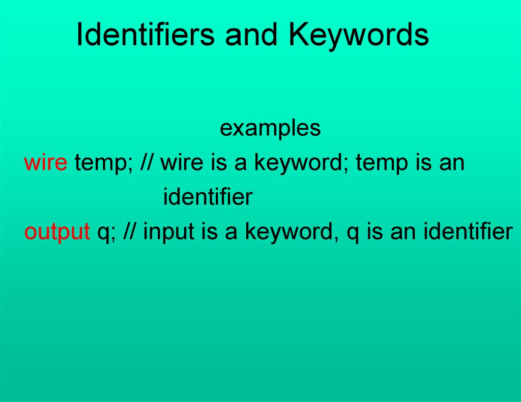
Identifiers and Keywordsexamples
wire temp; // wire is a keyword; temp is an
identifier
output q; // input is a keyword, q is an identifier
32.
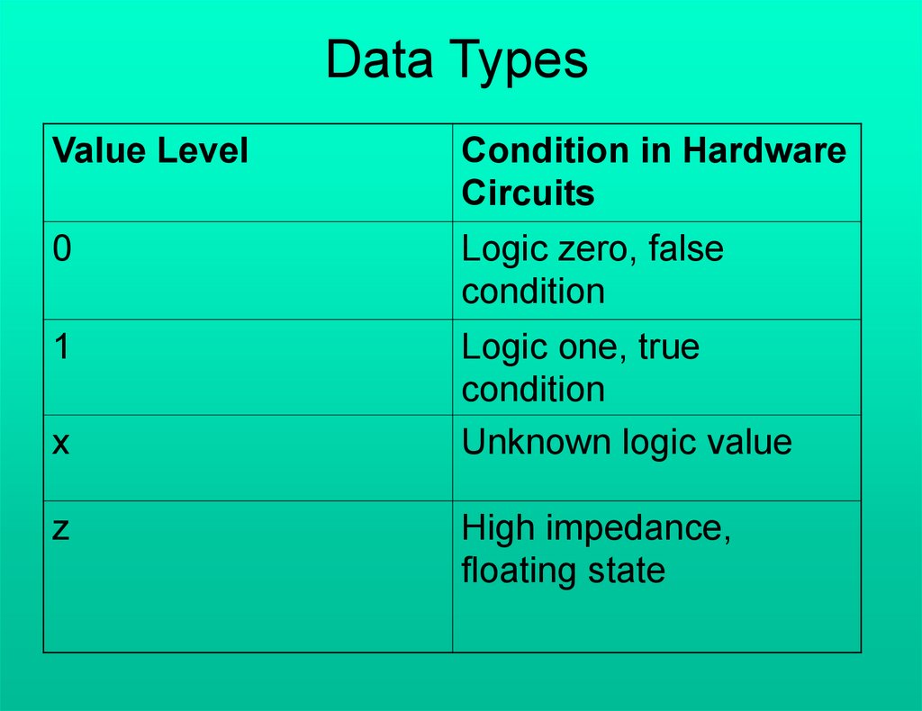
Data TypesValue Level
Condition in Hardware
Circuits
0
Logic zero, false
condition
1
Logic one, true
condition
Unknown logic value
x
z
High impedance,
floating state
33.
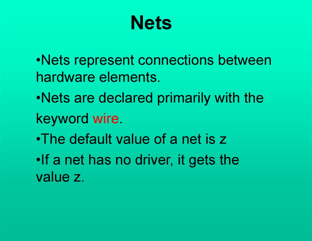
Nets•Nets represent connections between
hardware elements.
•Nets are declared primarily with the
keyword wire.
•The default value of a net is z
•If a net has no driver, it gets the
value z.
34.
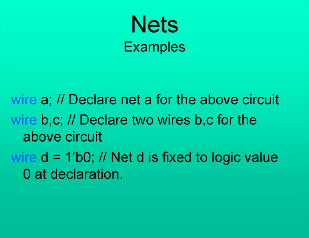
NetsExamples
wire a; // Declare net a for the above circuit
wire b,c; // Declare two wires b,c for the
above circuit
wire d = 1'b0; // Net d is fixed to logic value
0 at declaration.
35.
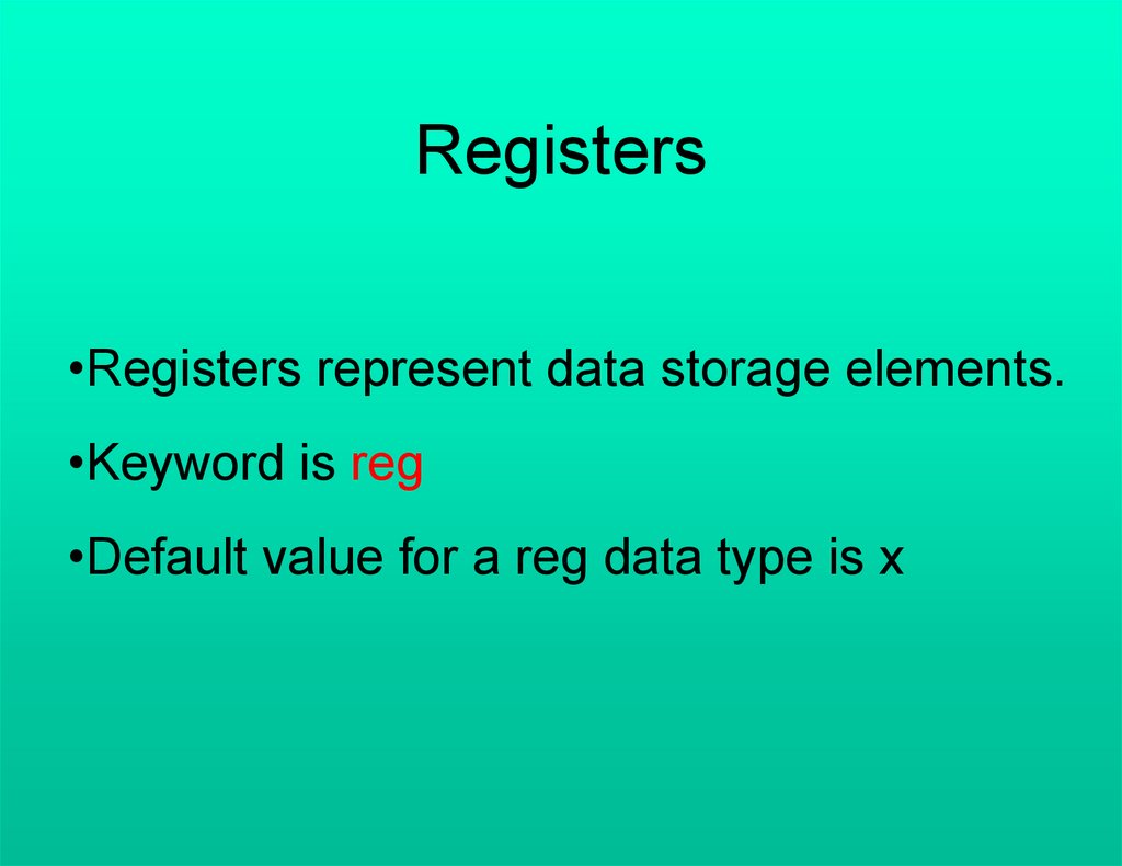
Registers•Registers represent data storage elements.
•Keyword is reg
•Default value for a reg data type is x
36.
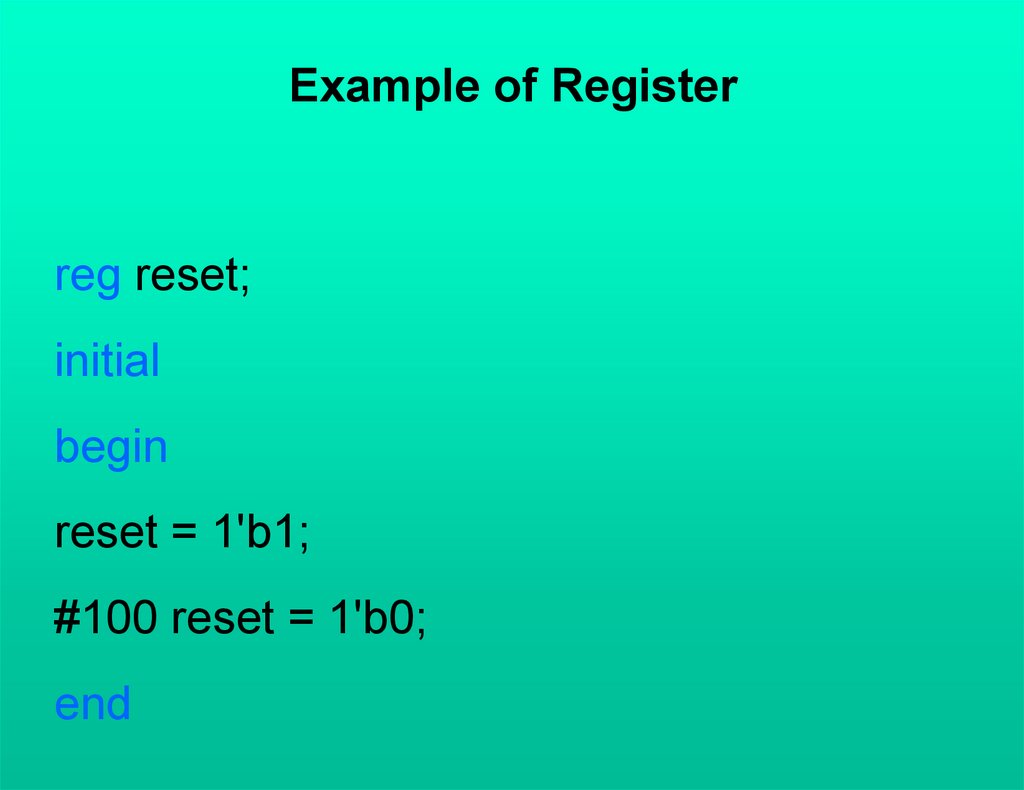
Example of Registerreg reset;
initial
begin
reset = 1'b1;
#100 reset = 1'b0;
end
37.
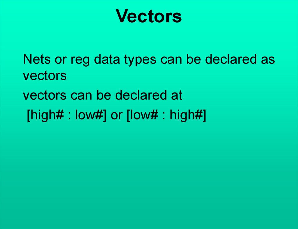
VectorsNets or reg data types can be declared as
vectors
vectors can be declared at
[high# : low#] or [low# : high#]
38.
Vectorsexamples
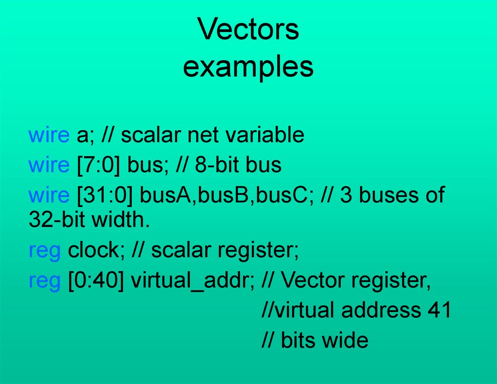
wire a; // scalar net variable
wire [7:0] bus; // 8-bit bus
wire [31:0] busA,busB,busC; // 3 buses of
32-bit width.
reg clock; // scalar register;
reg [0:40] virtual_addr; // Vector register,
//virtual address 41
// bits wide
39.
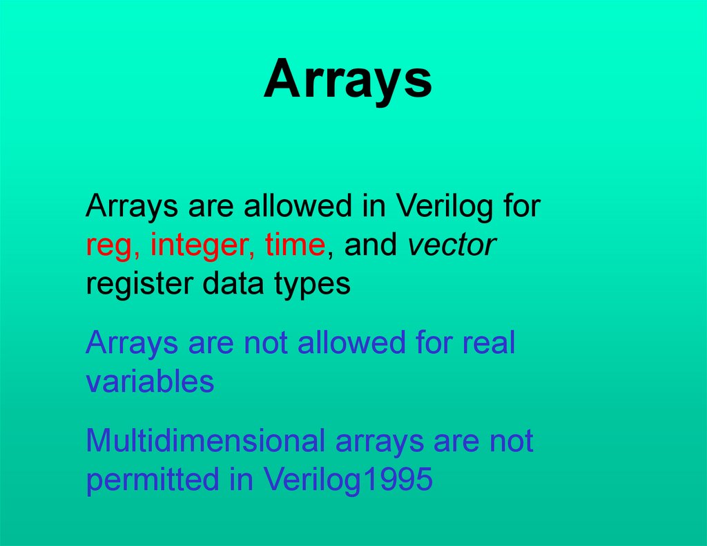
ArraysArrays are allowed in Verilog for
reg, integer, time, and vector
register data types
Arrays are not allowed for real
variables
Multidimensional arrays are not
permitted in Verilog1995
40.
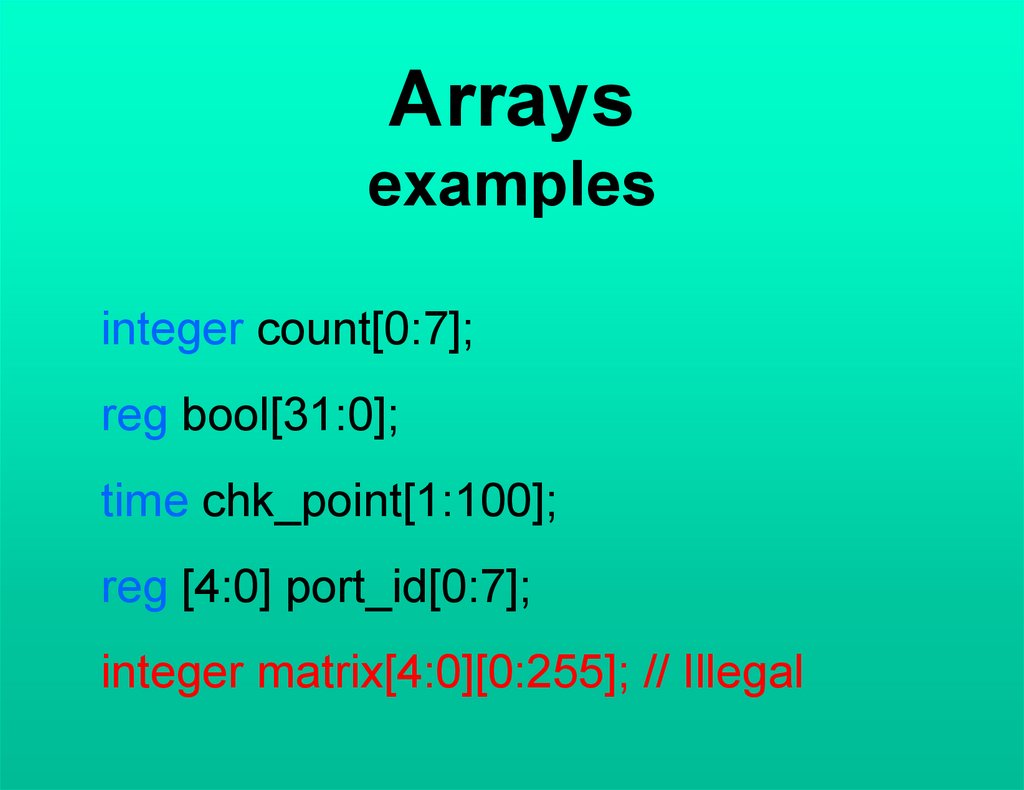
Arraysexamples
integer count[0:7];
reg bool[31:0];
time chk_point[1:100];
reg [4:0] port_id[0:7];
integer matrix[4:0][0:255]; // Illegal
41.
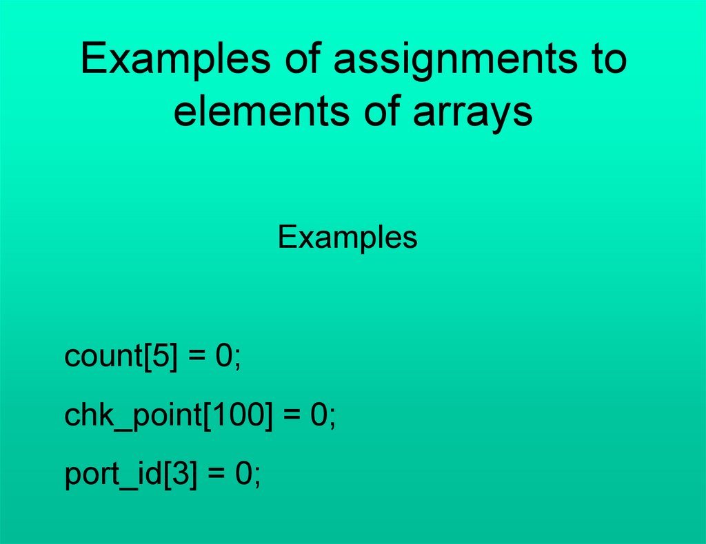
Examples of assignments toelements of arrays
Examples
count[5] = 0;
chk_point[100] = 0;
port_id[3] = 0;
42.
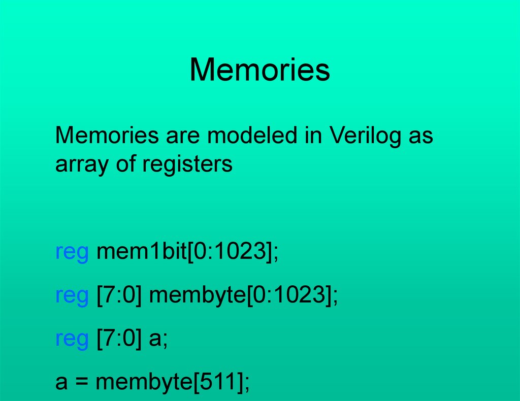
MemoriesMemories are modeled in Verilog as
array of registers
reg mem1bit[0:1023];
reg [7:0] membyte[0:1023];
reg [7:0] a;
a = membyte[511];
43.
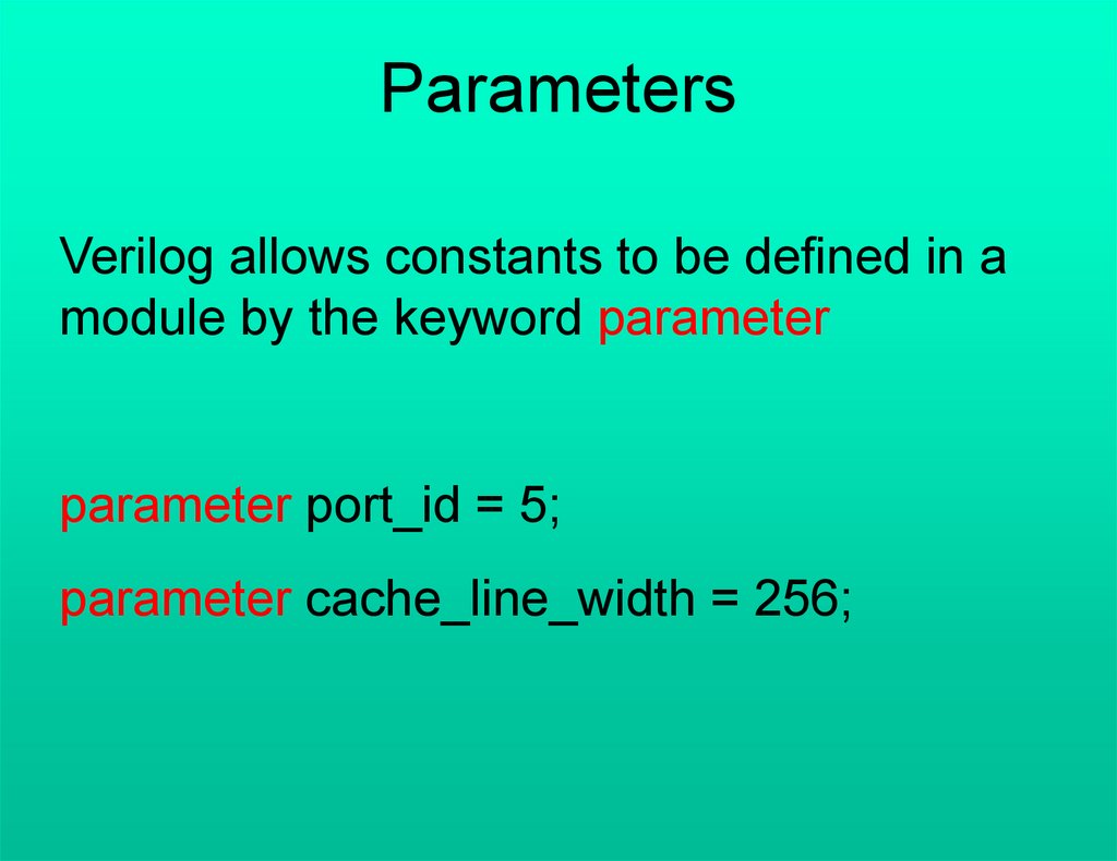
ParametersVerilog allows constants to be defined in a
module by the keyword parameter
parameter port_id = 5;
parameter cache_line_width = 256;
44.
Displaying information$display("Hello Verilog World");
$display($time);
reg [0:40] virtual_addr;
$display("At time %d virtual address is %h", $time,
virtual_addr);
$display("This string is displayed from %m level of
hierarchy");
$display("This is a \n multiline string with a %%
sign");
45.
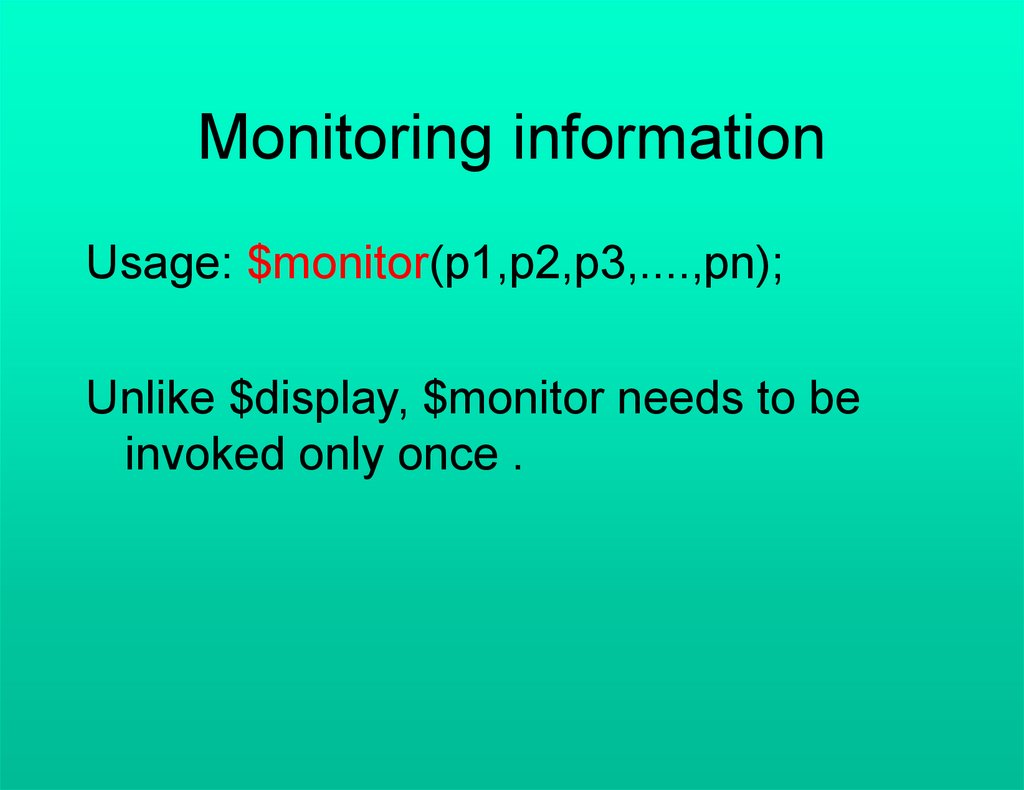
Monitoring informationUsage: $monitor(p1,p2,p3,....,pn);
Unlike $display, $monitor needs to be
invoked only once .
46.
Stopping and finishing in asimulation
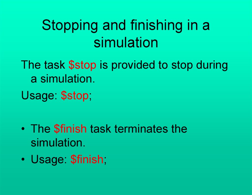
The task $stop is provided to stop during
a simulation.
Usage: $stop;
• The $finish task terminates the
simulation.
• Usage: $finish;
47.
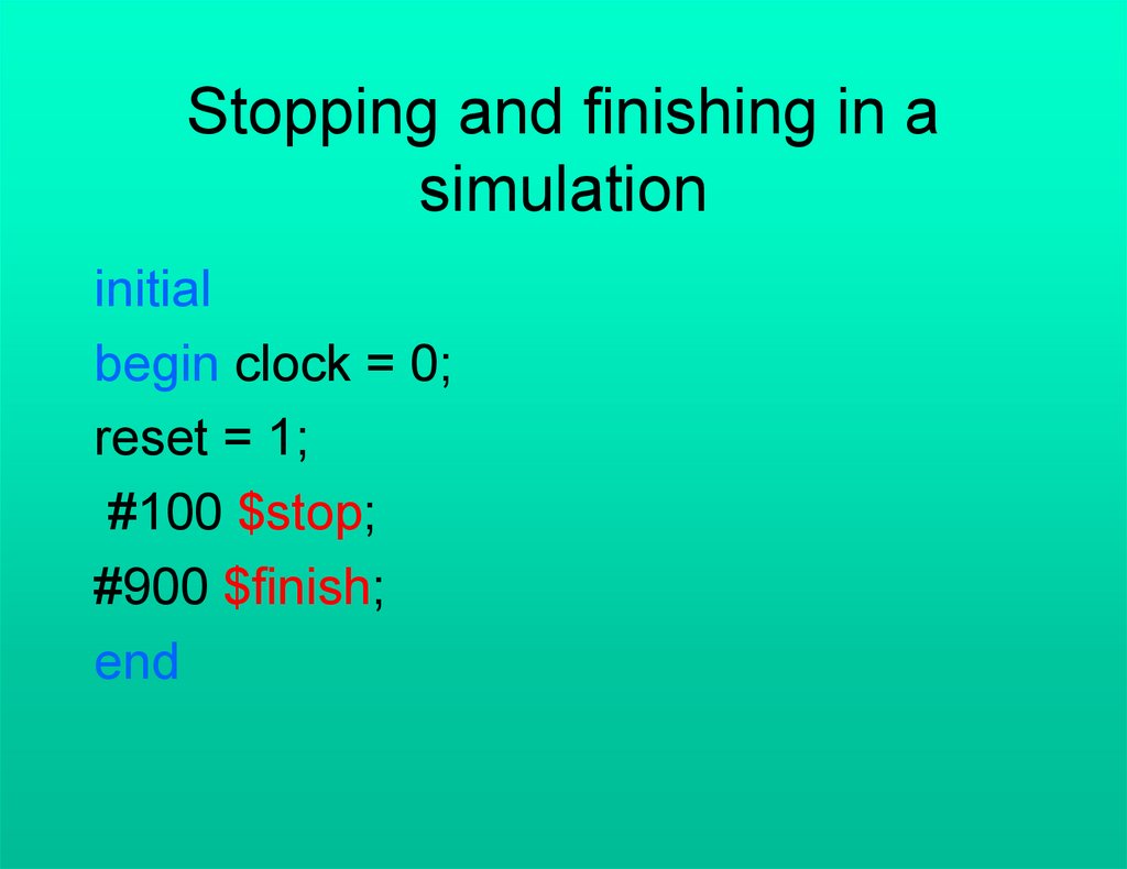
Stopping and finishing in asimulation
initial
begin clock = 0;
reset = 1;
#100 $stop;
#900 $finish;
end
48.
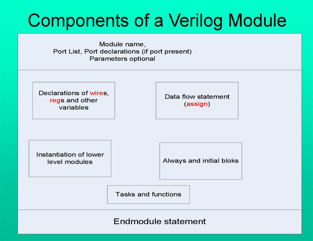
Components of a Verilog ModuleModule name,
Port List, Port declarations (if port present)
Parameters optional
Declarations of wires,
regs and other
variables
Instantiation of lower
level modules
Data flow statement
(assign)
Always and initial bloks
Tasks and functions
Endmodule statement
49.
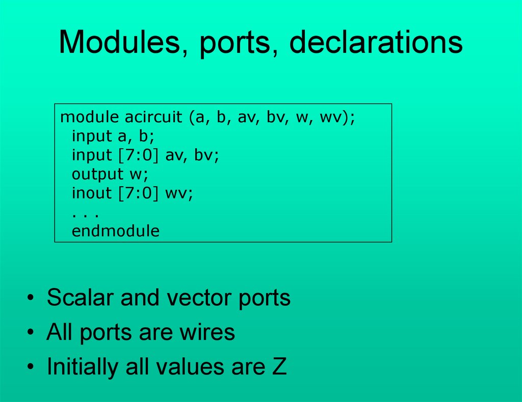
Modules, ports, declarationsmodule acircuit (a, b, av, bv, w, wv);
input a, b;
input [7:0] av, bv;
output w;
inout [7:0] wv;
...
endmodule
• Scalar and vector ports
• All ports are wires
• Initially all values are Z
50.
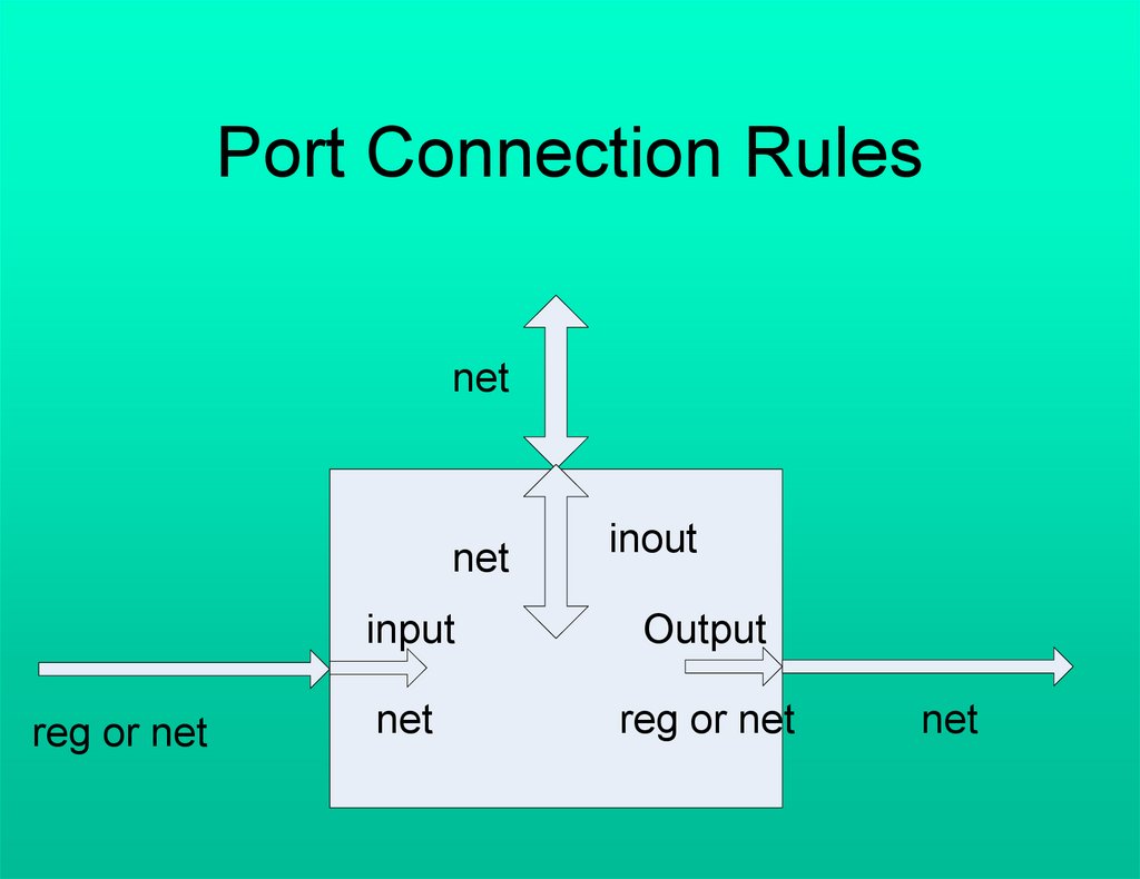
Port Connection Rulesnet
net
reg or net
inout
input
Output
net
reg or net
net
51.
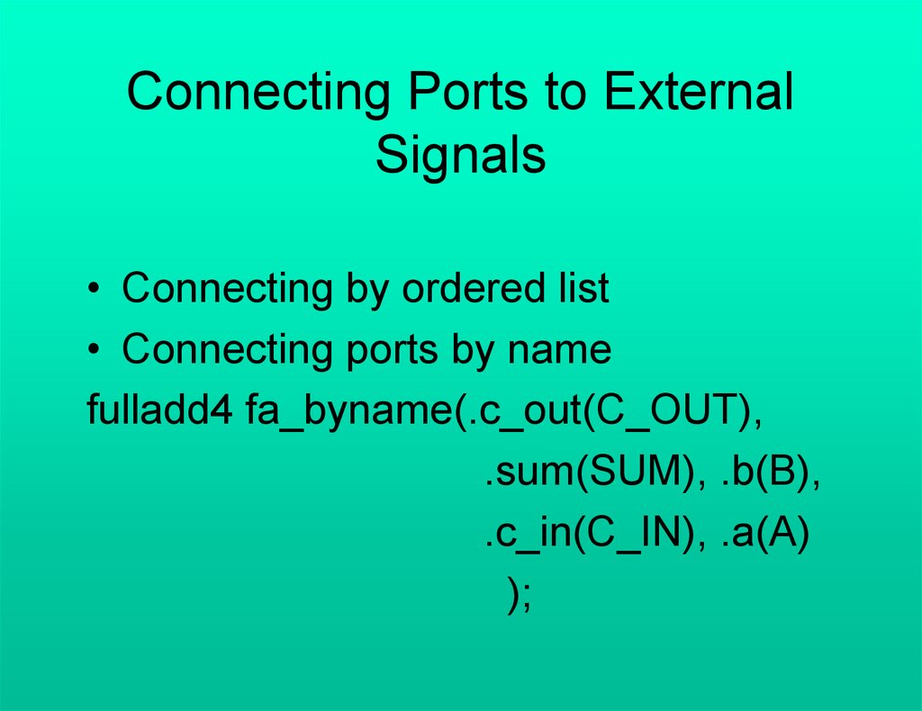
Connecting Ports to ExternalSignals
• Connecting by ordered list
• Connecting ports by name
fulladd4 fa_byname(.c_out(C_OUT),
.sum(SUM), .b(B),
.c_in(C_IN), .a(A)
);
52.
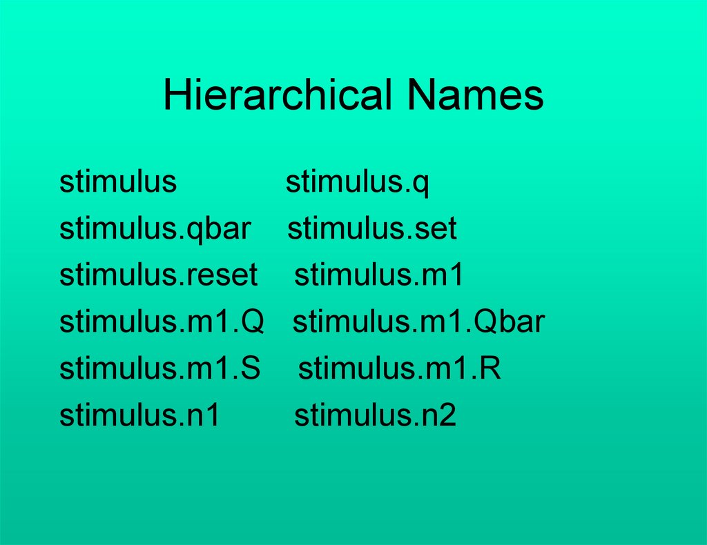
Hierarchical Namesstimulus
stimulus.qbar
stimulus.reset
stimulus.m1.Q
stimulus.m1.S
stimulus.n1
stimulus.q
stimulus.set
stimulus.m1
stimulus.m1.Qbar
stimulus.m1.R
stimulus.n2
53.
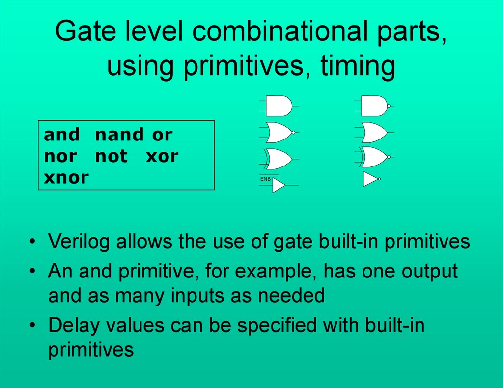
Gate level combinational parts,using primitives, timing
and nand or
nor not xor
xnor
ENB
• Verilog allows the use of gate built-in primitives
• An and primitive, for example, has one output
and as many inputs as needed
• Delay values can be specified with built-in
primitives
54.
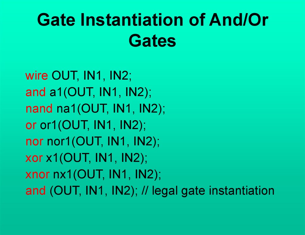
Gate Instantiation of And/OrGates
wire OUT, IN1, IN2;
and a1(OUT, IN1, IN2);
nand na1(OUT, IN1, IN2);
or or1(OUT, IN1, IN2);
nor nor1(OUT, IN1, IN2);
xor x1(OUT, IN1, IN2);
xnor nx1(OUT, IN1, IN2);
and (OUT, IN1, IN2); // legal gate instantiation
55.
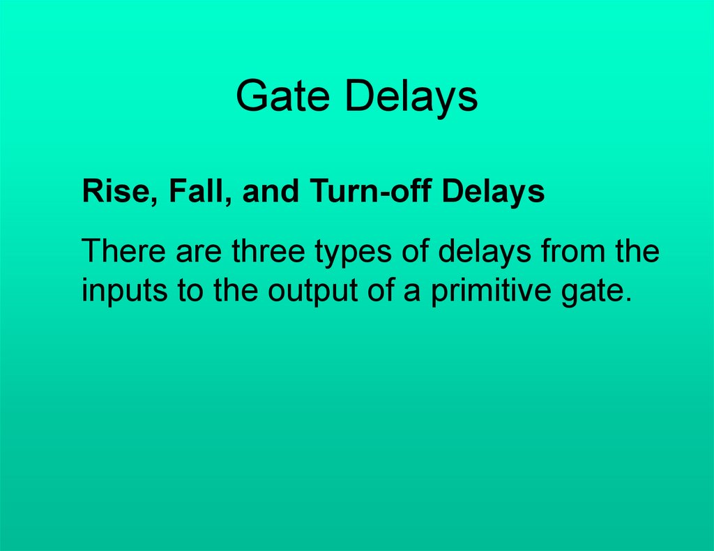
Gate DelaysRise, Fall, and Turn-off Delays
There are three types of delays from the
inputs to the output of a primitive gate.
56.
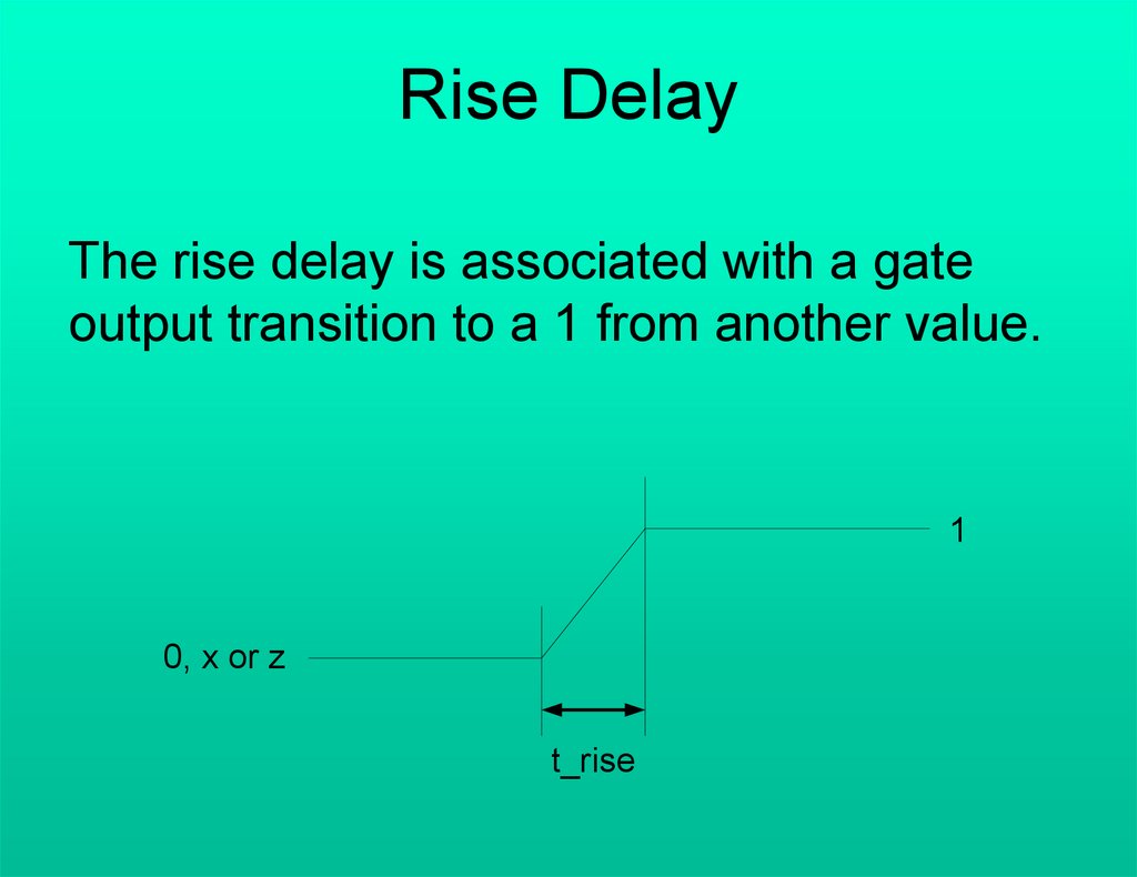
Rise DelayThe rise delay is associated with a gate
output transition to a 1 from another value.
1
0, x or z
t_rise
57.
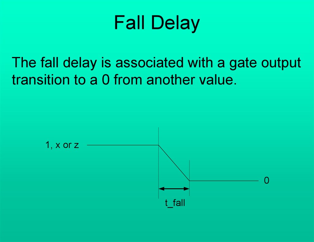
Fall DelayThe fall delay is associated with a gate output
transition to a 0 from another value.
1, x or z
0
t_fall
58.
Turn-off delayThe turn-off delay is associated with a gate
output transition to the high impedance value
(z) from another value.
59.
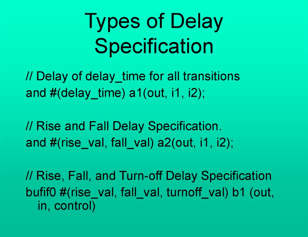
Types of DelaySpecification
// Delay of delay_time for all transitions
and #(delay_time) a1(out, i1, i2);
// Rise and Fall Delay Specification.
and #(rise_val, fall_val) a2(out, i1, i2);
// Rise, Fall, and Turn-off Delay Specification
bufif0 #(rise_val, fall_val, turnoff_val) b1 (out,
in, control)
60.
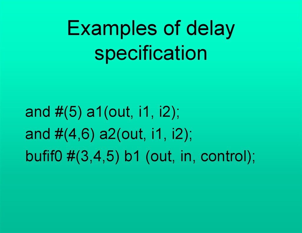
Examples of delayspecification
and #(5) a1(out, i1, i2);
and #(4,6) a2(out, i1, i2);
bufif0 #(3,4,5) b1 (out, in, control);
61.
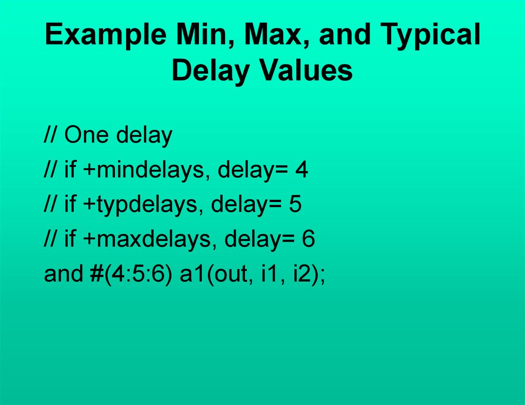
Example Min, Max, and TypicalDelay Values
// One delay
// if +mindelays, delay= 4
// if +typdelays, delay= 5
// if +maxdelays, delay= 6
and #(4:5:6) a1(out, i1, i2);
62.
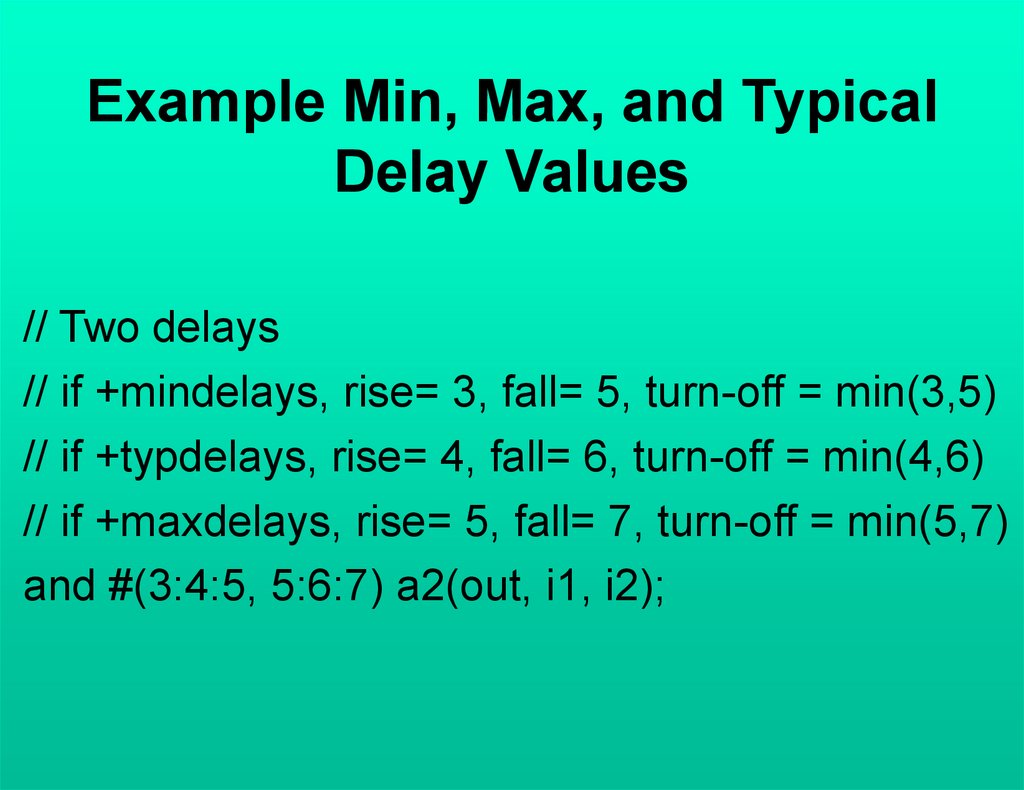
Example Min, Max, and TypicalDelay Values
// Two delays
// if +mindelays, rise= 3, fall= 5, turn-off = min(3,5)
// if +typdelays, rise= 4, fall= 6, turn-off = min(4,6)
// if +maxdelays, rise= 5, fall= 7, turn-off = min(5,7)
and #(3:4:5, 5:6:7) a2(out, i1, i2);
63.
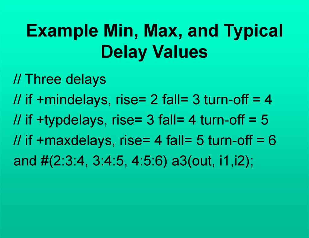
Example Min, Max, and TypicalDelay Values
// Three delays
// if +mindelays, rise= 2 fall= 3 turn-off = 4
// if +typdelays, rise= 3 fall= 4 turn-off = 5
// if +maxdelays, rise= 4 fall= 5 turn-off = 6
and #(2:3:4, 3:4:5, 4:5:6) a3(out, i1,i2);
64.
Delay ExampleD
a
b
c
#5
e
#4
out
65.
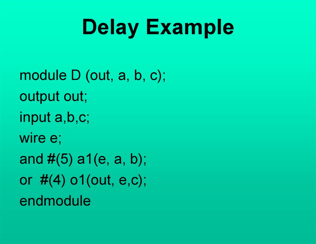
Delay Examplemodule D (out, a, b, c);
output out;
input a,b,c;
wire e;
and #(5) a1(e, a, b);
or #(4) o1(out, e,c);
endmodule
66.
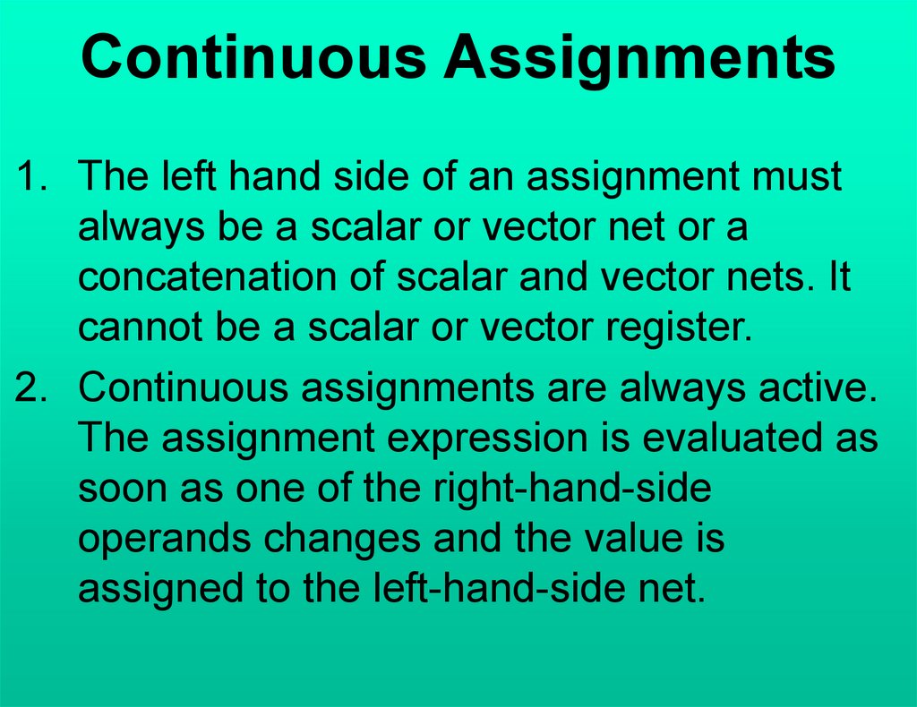
Continuous Assignments1. The left hand side of an assignment must
always be a scalar or vector net or a
concatenation of scalar and vector nets. It
cannot be a scalar or vector register.
2. Continuous assignments are always active.
The assignment expression is evaluated as
soon as one of the right-hand-side
operands changes and the value is
assigned to the left-hand-side net.
67.
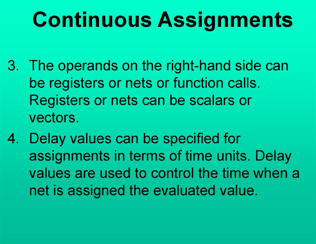
Continuous Assignments3. The operands on the right-hand side can
be registers or nets or function calls.
Registers or nets can be scalars or
vectors.
4. Delay values can be specified for
assignments in terms of time units. Delay
values are used to control the time when a
net is assigned the evaluated value.
68.
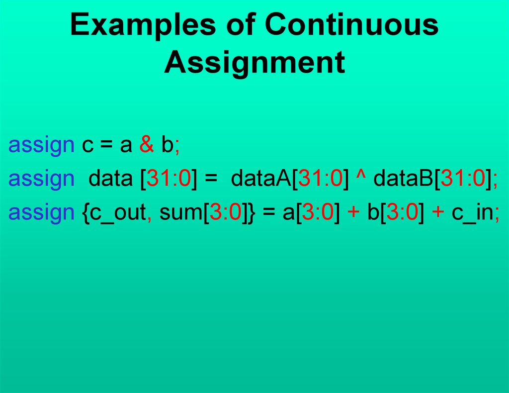
Examples of ContinuousAssignment
assign c = a & b;
assign data [31:0] = dataA[31:0] ^ dataB[31:0];
assign {c_out, sum[3:0]} = a[3:0] + b[3:0] + c_in;
69.
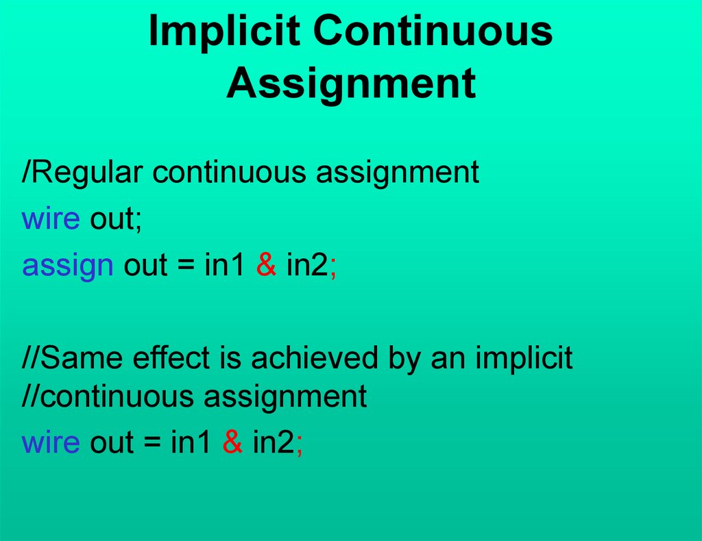
Implicit ContinuousAssignment
/Regular continuous assignment
wire out;
assign out = in1 & in2;
//Same effect is achieved by an implicit
//continuous assignment
wire out = in1 & in2;
70.
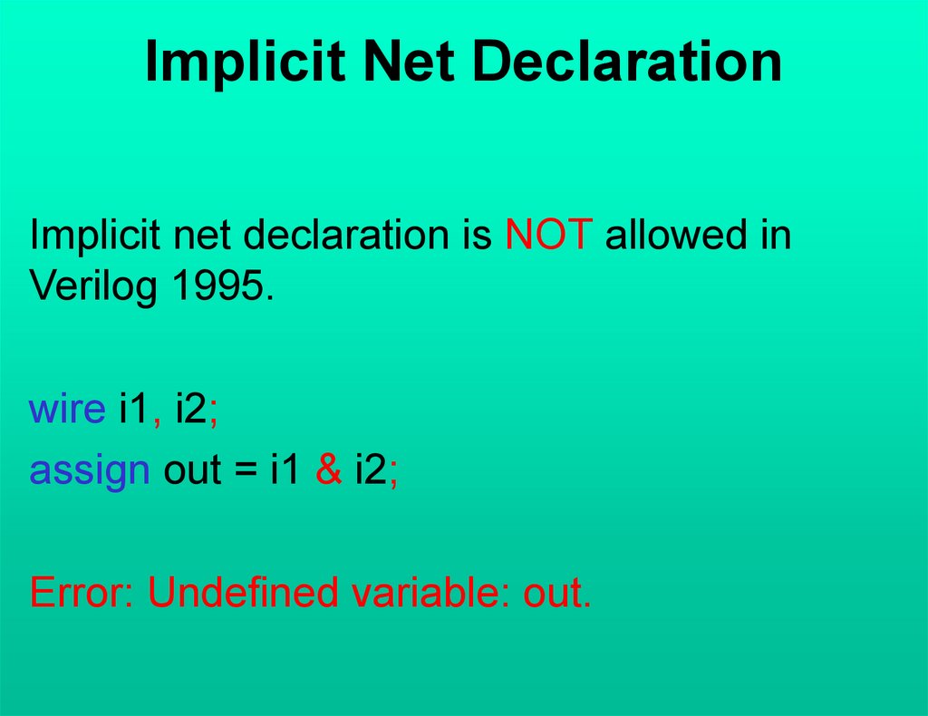
Implicit Net DeclarationImplicit net declaration is NOT allowed in
Verilog 1995.
wire i1, i2;
assign out = i1 & i2;
Error: Undefined variable: out.
71.
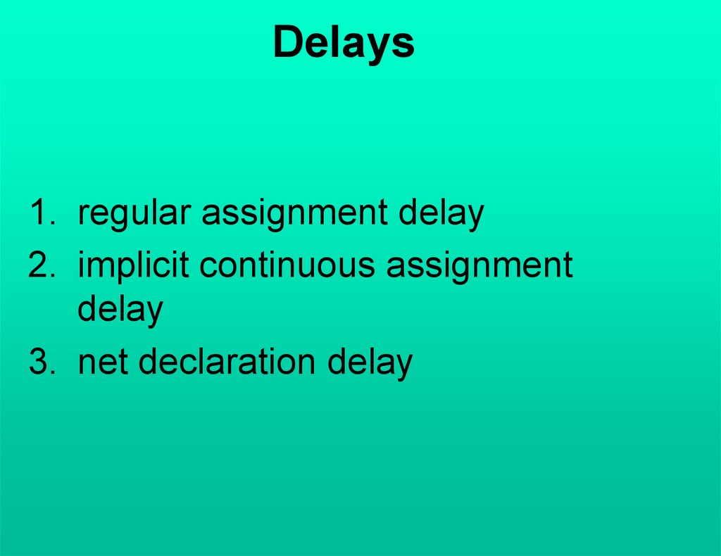
Delays1. regular assignment delay
2. implicit continuous assignment
delay
3. net declaration delay
72.
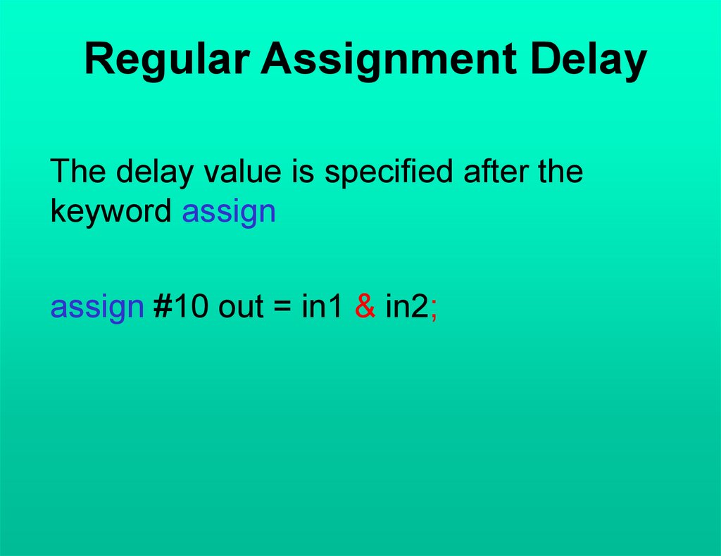
Regular Assignment DelayThe delay value is specified after the
keyword assign
assign #10 out = in1 & in2;
73.
Implicit ContinuousAssignment Delay
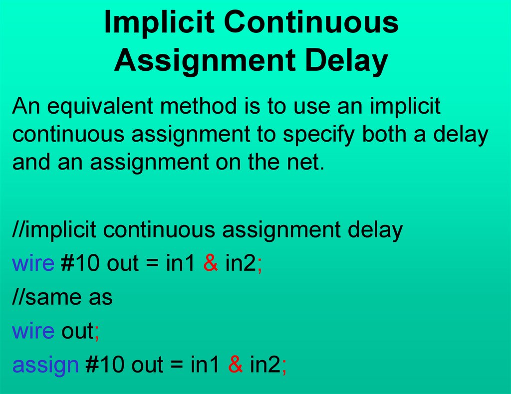
An equivalent method is to use an implicit
continuous assignment to specify both a delay
and an assignment on the net.
//implicit continuous assignment delay
wire #10 out = in1 & in2;
//same as
wire out;
assign #10 out = in1 & in2;
74.
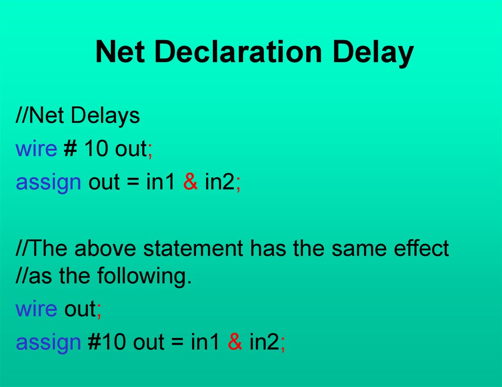
Net Declaration Delay//Net Delays
wire # 10 out;
assign out = in1 & in2;
//The above statement has the same effect
//as the following.
wire out;
assign #10 out = in1 & in2;
75.
ExpressionsExpressions are constructs that combine
operators and operands to produce a result.
a^b
addr1[20:17] + addr2[20:17]
in1 | in2
76.
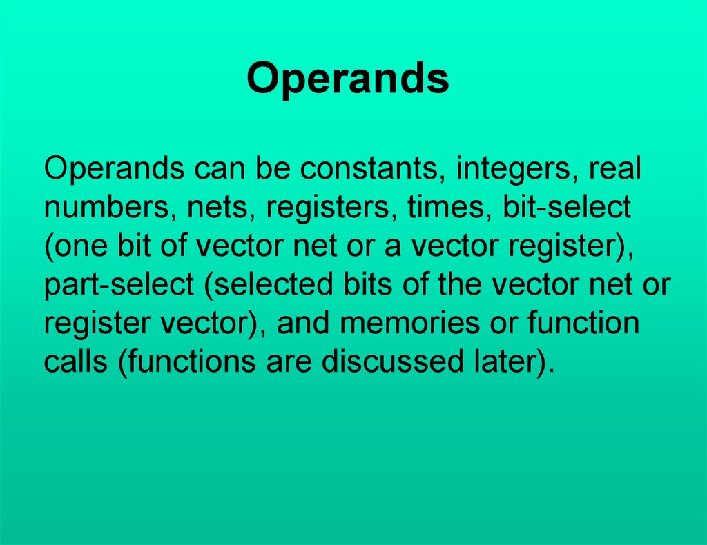
OperandsOperands can be constants, integers, real
numbers, nets, registers, times, bit-select
(one bit of vector net or a vector register),
part-select (selected bits of the vector net or
register vector), and memories or function
calls (functions are discussed later).
77.
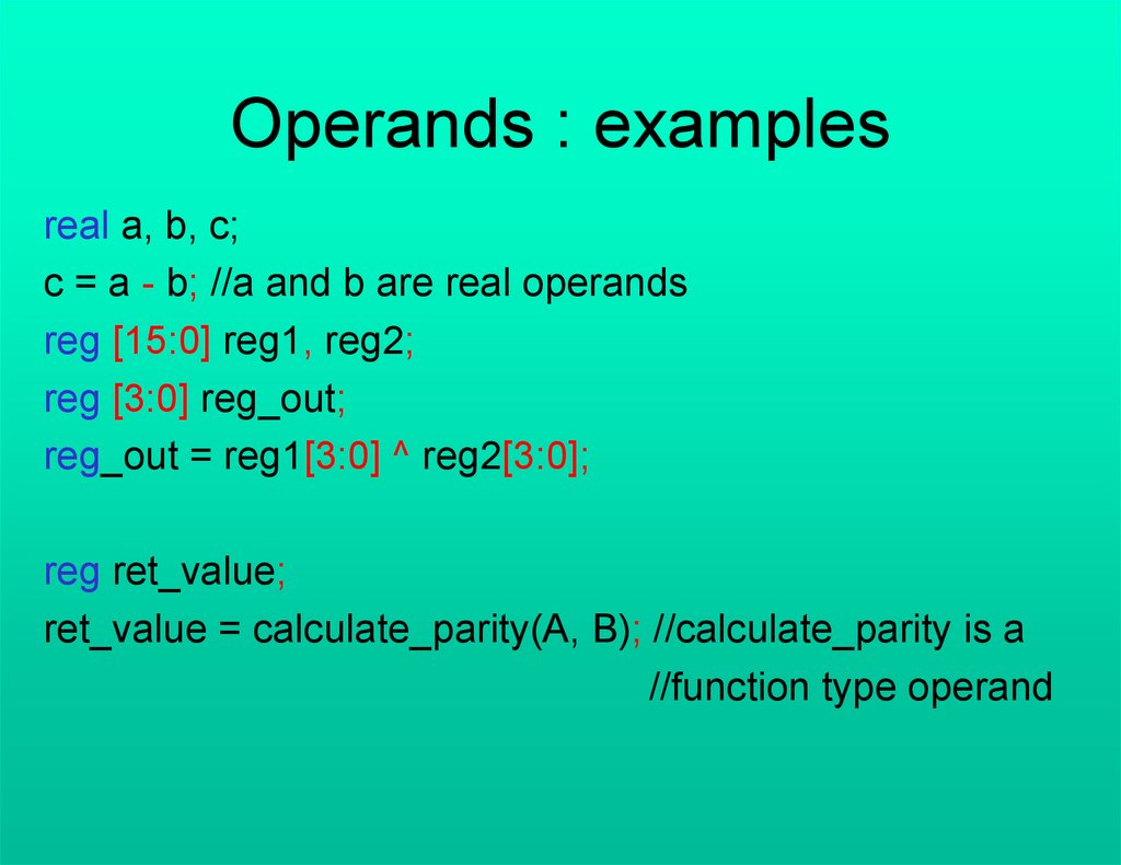
Operands : examplesreal a, b, c;
c = a - b; //a and b are real operands
reg [15:0] reg1, reg2;
reg [3:0] reg_out;
reg_out = reg1[3:0] ^ reg2[3:0];
reg ret_value;
ret_value = calculate_parity(A, B); //calculate_parity is a
//function type operand
78.
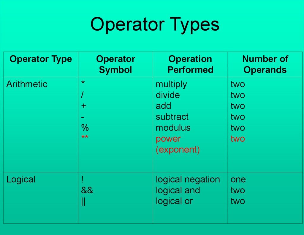
Operator TypesOperator Type
Operator
Symbol
Operation
Performed
Number of
Operands
Arithmetic
*
/
+
%
**
multiply
divide
add
subtract
modulus
power
(exponent)
two
two
two
two
two
two
Logical
!
&&
||
logical negation
logical and
logical or
one
two
two
79.
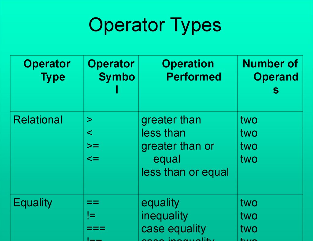
Operator TypesOperator
Type
Operator
Symbo
l
Operation
Performed
Number of
Operand
s
Relational
>
<
>=
<=
greater than
less than
greater than or
equal
less than or equal
two
two
two
two
Equality
==
!=
===
equality
inequality
case equality
two
two
two
80.
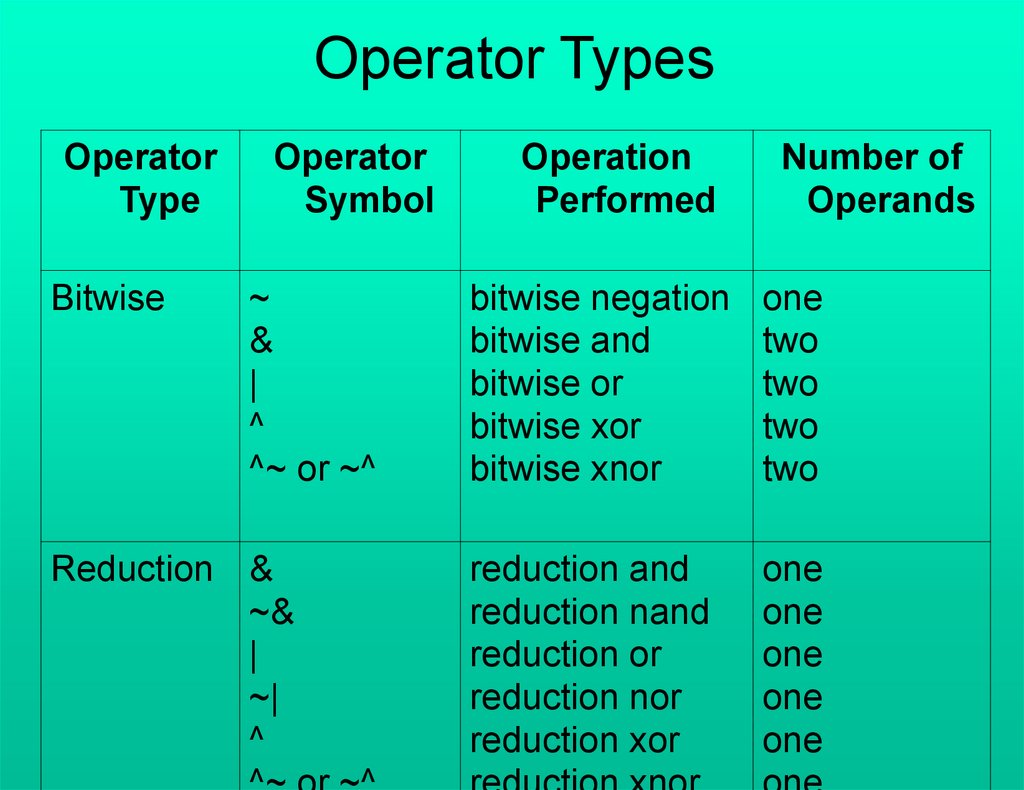
Operator TypesOperator
Type
Bitwise
Operator
Symbol
~
&
|
^
^~ or ~^
Reduction &
~&
|
~|
^
Operation
Performed
Number of
Operands
bitwise negation
bitwise and
bitwise or
bitwise xor
bitwise xnor
one
two
two
two
two
reduction and
reduction nand
reduction or
reduction nor
reduction xor
one
one
one
one
one
81.
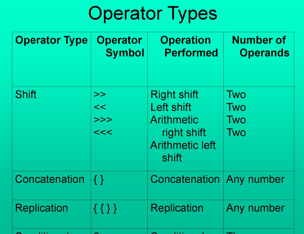
Operator TypesOperator Type Operator
Symbol
Shift
>>
<<
>>>
<<<
Operation
Performed
Right shift
Left shift
Arithmetic
right shift
Arithmetic left
shift
Number of
Operands
Two
Two
Two
Two
Concatenation { }
Concatenation Any number
Replication
Replication
{{}}
Any number
82.
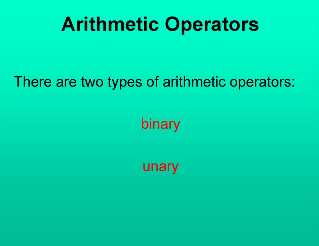
Arithmetic OperatorsThere are two types of arithmetic operators:
binary
unary
83.
Binary operatorsBinary arithmetic operators are
multiply (*)
divide (/)
add (+)
subtract (-)
power (**)
modulus (%).
Binary operators take two operands.
84.
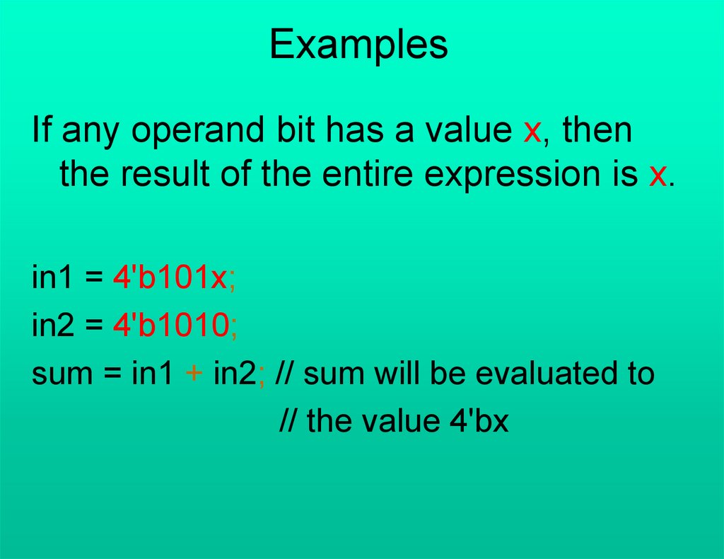
ExamplesIf any operand bit has a value x, then
the result of the entire expression is x.
in1 = 4'b101x;
in2 = 4'b1010;
sum = in1 + in2; // sum will be evaluated to
// the value 4'bx
85.
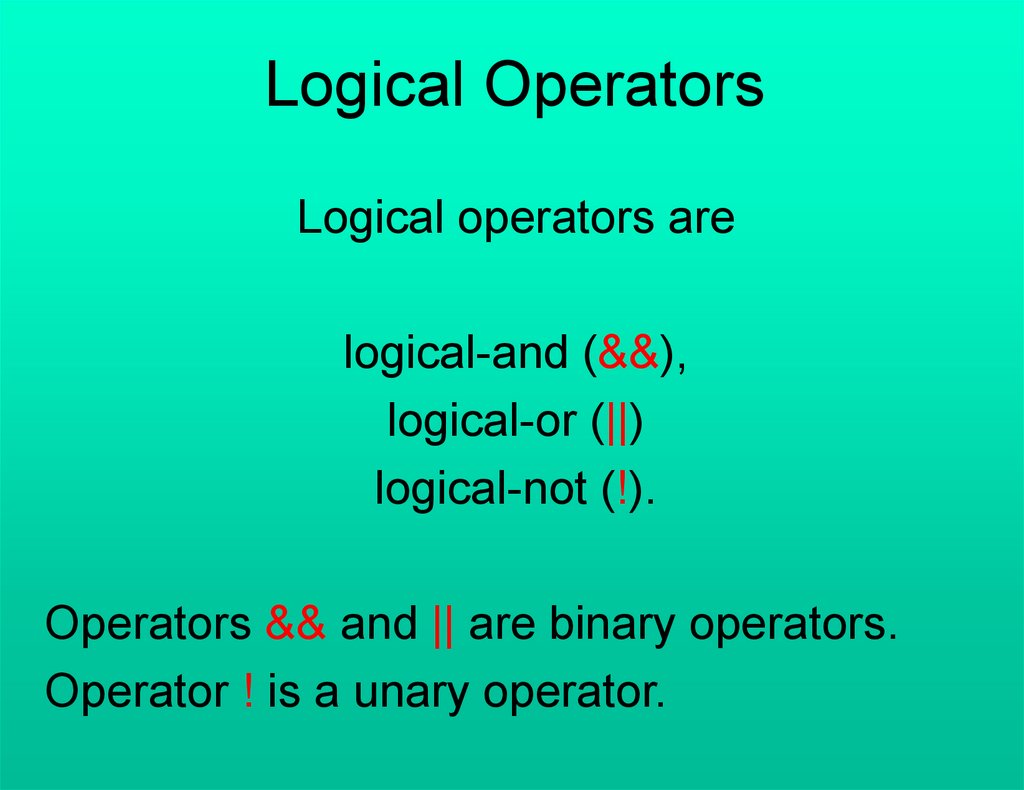
Logical OperatorsLogical operators are
logical-and (&&),
logical-or (||)
logical-not (!).
Operators && and || are binary operators.
Operator ! is a unary operator.
86.
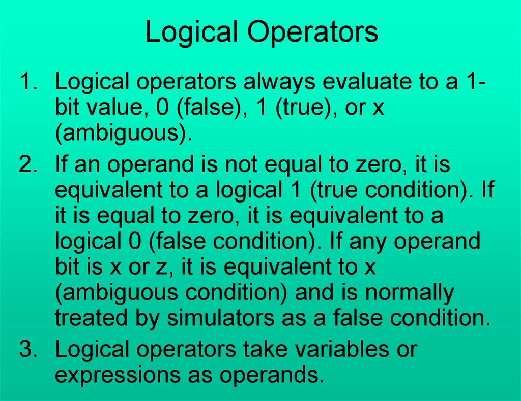
Logical Operators1. Logical operators always evaluate to a 1bit value, 0 (false), 1 (true), or x
(ambiguous).
2. If an operand is not equal to zero, it is
equivalent to a logical 1 (true condition). If
it is equal to zero, it is equivalent to a
logical 0 (false condition). If any operand
bit is x or z, it is equivalent to x
(ambiguous condition) and is normally
treated by simulators as a false condition.
3. Logical operators take variables or
expressions as operands.
87.
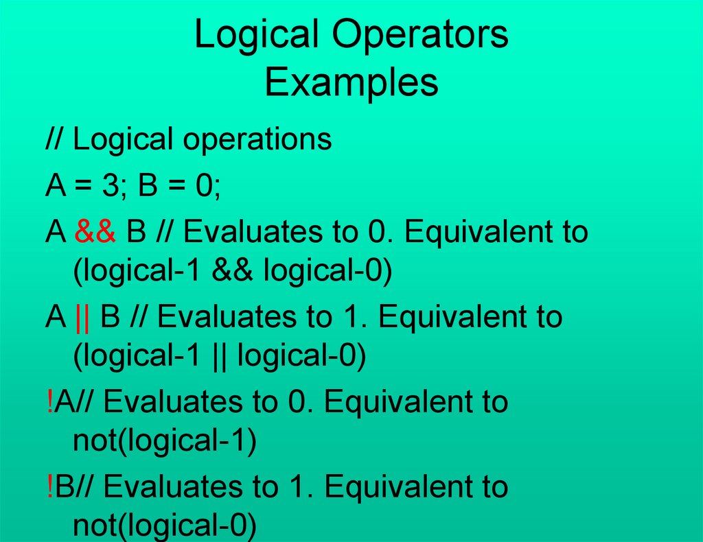
Logical OperatorsExamples
// Logical operations
A = 3; B = 0;
A && B // Evaluates to 0. Equivalent to
(logical-1 && logical-0)
A || B // Evaluates to 1. Equivalent to
(logical-1 || logical-0)
!A// Evaluates to 0. Equivalent to
not(logical-1)
!B// Evaluates to 1. Equivalent to
not(logical-0)
88.
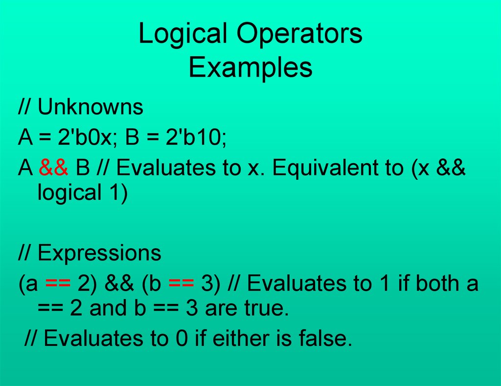
Logical OperatorsExamples
// Unknowns
A = 2'b0x; B = 2'b10;
A && B // Evaluates to x. Equivalent to (x &&
logical 1)
// Expressions
(a == 2) && (b == 3) // Evaluates to 1 if both a
== 2 and b == 3 are true.
// Evaluates to 0 if either is false.
89.
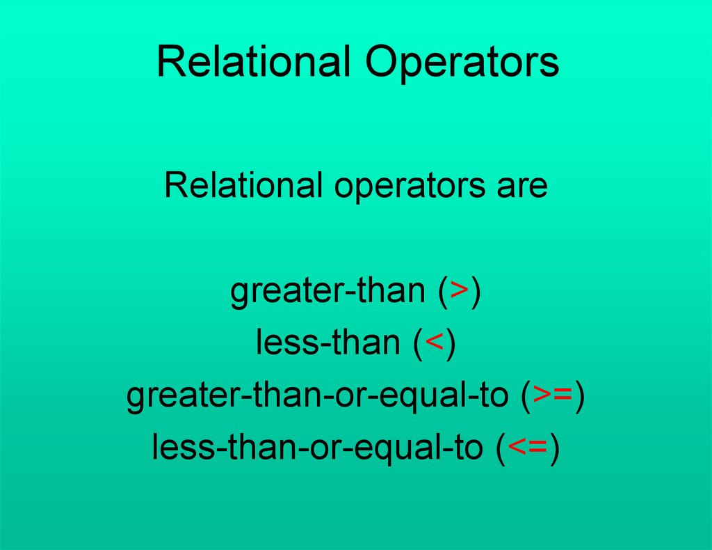
Relational OperatorsRelational operators are
greater-than (>)
less-than (<)
greater-than-or-equal-to (>=)
less-than-or-equal-to (<=)
90.
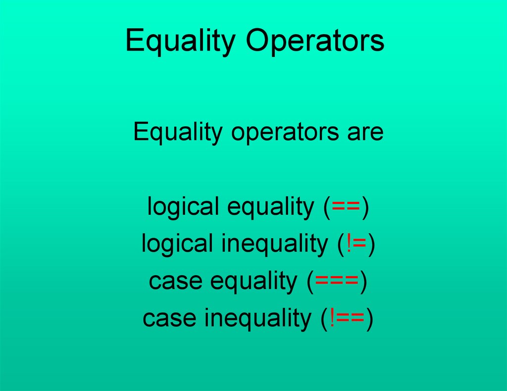
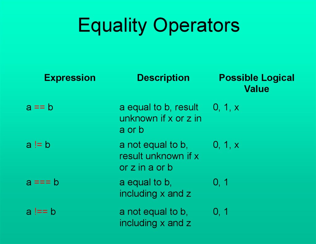
Equality OperatorsEquality operators are
logical equality (==)
logical inequality (!=)
case equality (===)
case inequality (!==)
91.
Equality OperatorsExpression
Description
Possible Logical
Value
a == b
a equal to b, result
unknown if x or z in
a or b
0, 1, x
a != b
a not equal to b,
result unknown if x
or z in a or b
0, 1, x
a === b
a equal to b,
including x and z
0, 1
a !== b
a not equal to b,
including x and z
0, 1
92.
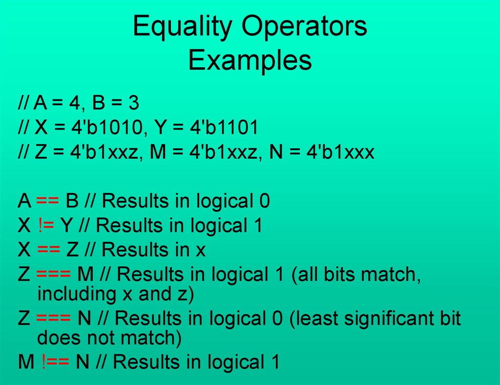
Equality OperatorsExamples
// A = 4, B = 3
// X = 4'b1010, Y = 4'b1101
// Z = 4'b1xxz, M = 4'b1xxz, N = 4'b1xxx
A == B // Results in logical 0
X != Y // Results in logical 1
X == Z // Results in x
Z === M // Results in logical 1 (all bits match,
including x and z)
Z === N // Results in logical 0 (least significant bit
does not match)
M !== N // Results in logical 1
93.
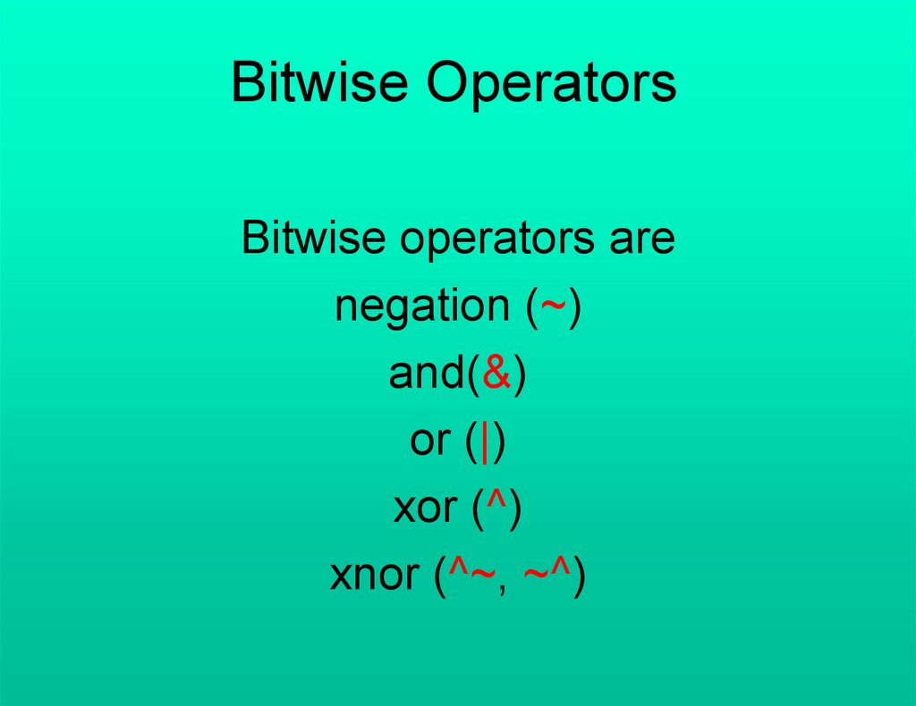
Bitwise OperatorsBitwise operators are
negation (~)
and(&)
or (|)
xor (^)
xnor (^~, ~^)
94.
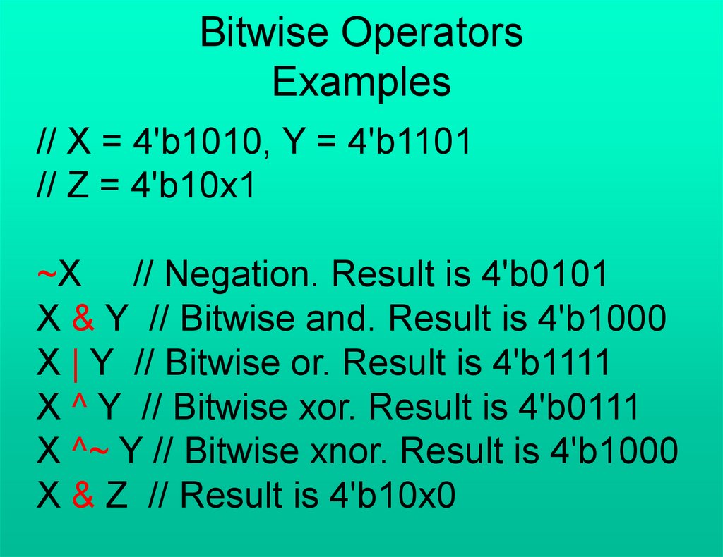
Bitwise OperatorsExamples
// X = 4'b1010, Y = 4'b1101
// Z = 4'b10x1
~X // Negation. Result is 4'b0101
X & Y // Bitwise and. Result is 4'b1000
X | Y // Bitwise or. Result is 4'b1111
X ^ Y // Bitwise xor. Result is 4'b0111
X ^~ Y // Bitwise xnor. Result is 4'b1000
X & Z // Result is 4'b10x0
95.
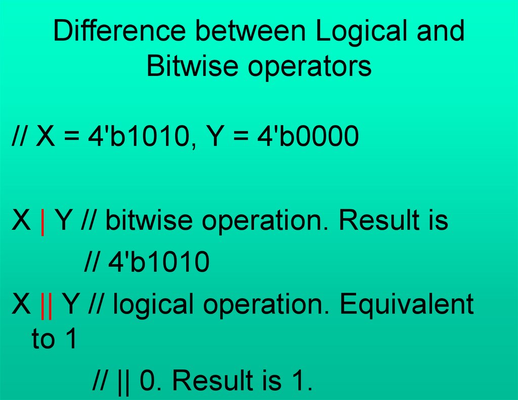
Difference between Logical andBitwise operators
// X = 4'b1010, Y = 4'b0000
X | Y // bitwise operation. Result is
// 4'b1010
X || Y // logical operation. Equivalent
to 1
// || 0. Result is 1.
96.
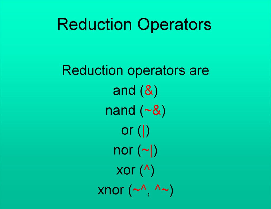
Reduction OperatorsReduction operators are
and (&)
nand (~&)
or (|)
nor (~|)
xor (^)
xnor (~^, ^~)
97.
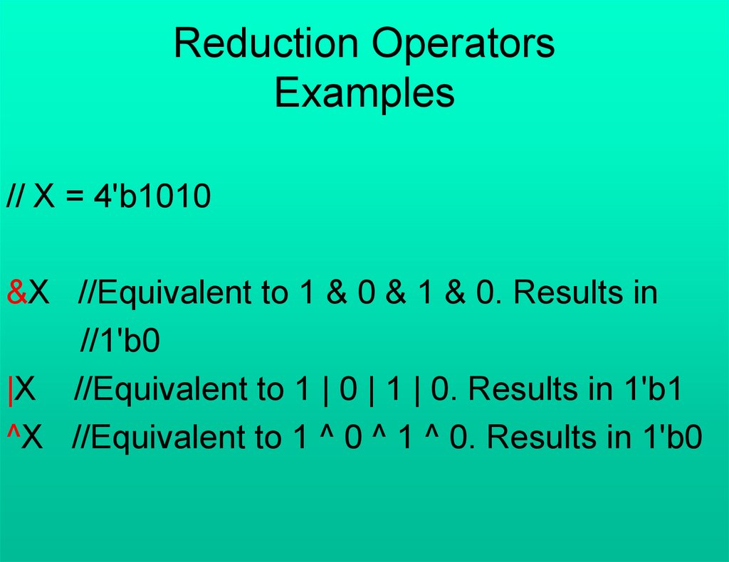
Reduction OperatorsExamples
// X = 4'b1010
&X //Equivalent to 1 & 0 & 1 & 0. Results in
//1'b0
|X //Equivalent to 1 | 0 | 1 | 0. Results in 1'b1
^X //Equivalent to 1 ^ 0 ^ 1 ^ 0. Results in 1'b0
98.
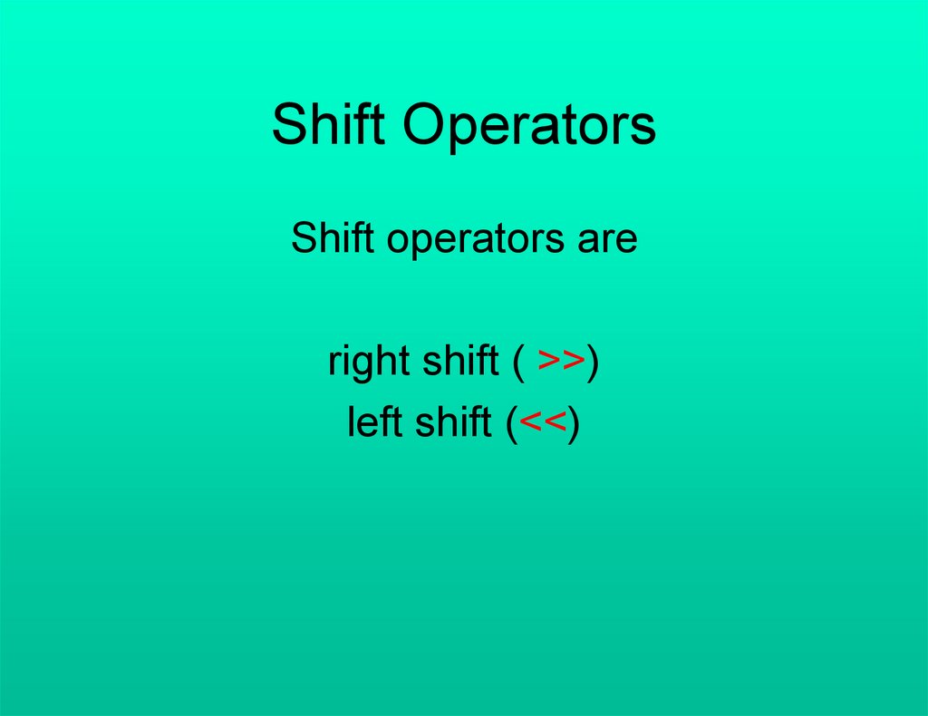
Shift OperatorsShift operators are
right shift ( >>)
left shift (<<)
99.
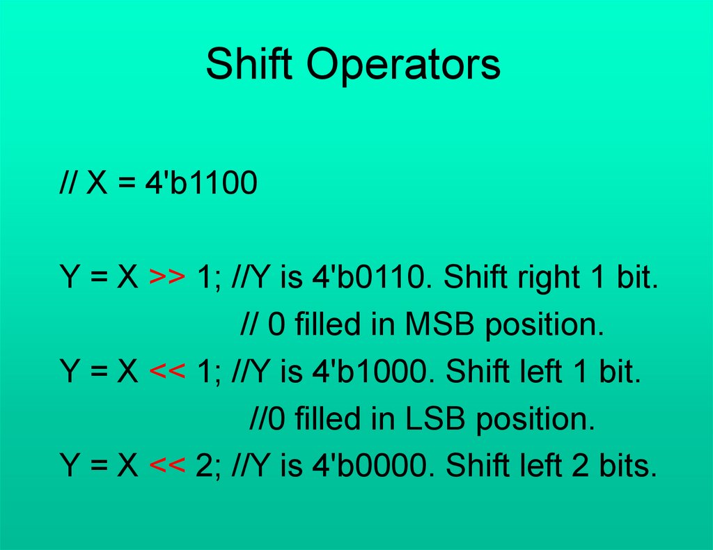
Shift Operators// X = 4'b1100
Y = X >> 1; //Y is 4'b0110. Shift right 1 bit.
// 0 filled in MSB position.
Y = X << 1; //Y is 4'b1000. Shift left 1 bit.
//0 filled in LSB position.
Y = X << 2; //Y is 4'b0000. Shift left 2 bits.
100.
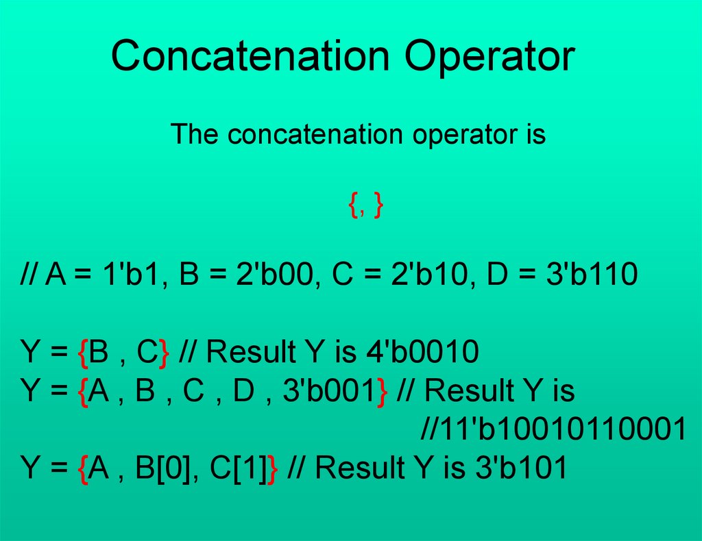
Concatenation OperatorThe concatenation operator is
{, }
// A = 1'b1, B = 2'b00, C = 2'b10, D = 3'b110
Y = {B , C} // Result Y is 4'b0010
Y = {A , B , C , D , 3'b001} // Result Y is
//11'b10010110001
Y = {A , B[0], C[1]} // Result Y is 3'b101
101.
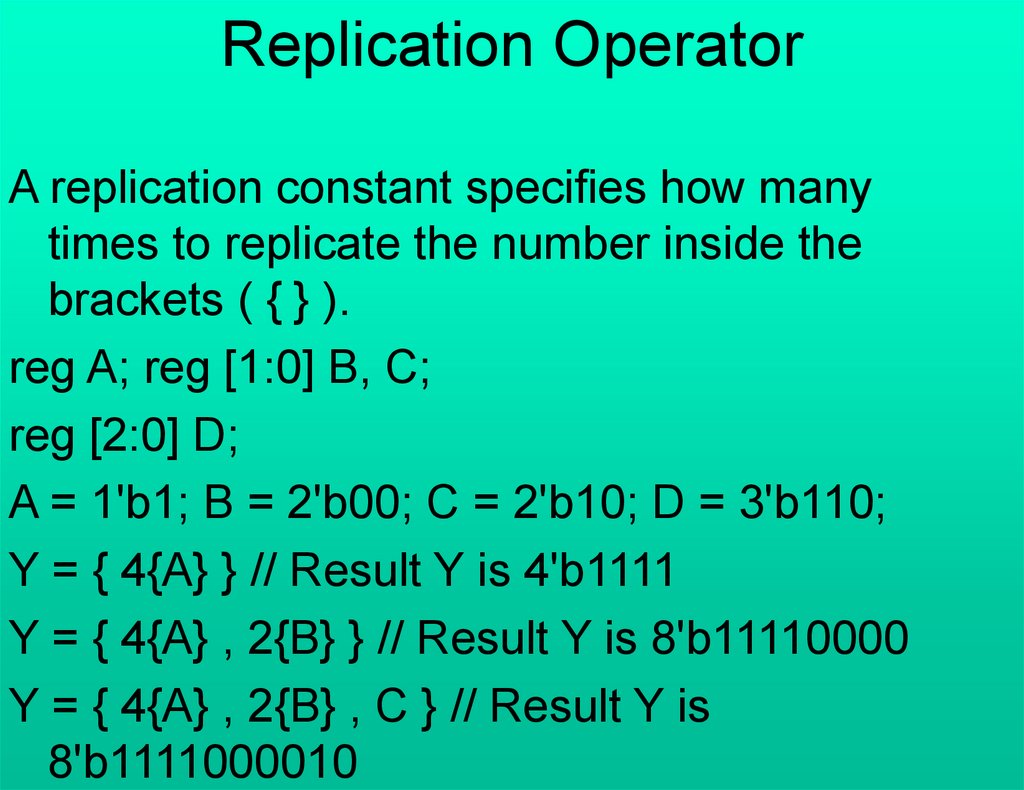
Replication OperatorA replication constant specifies how many
times to replicate the number inside the
brackets ( { } ).
reg A; reg [1:0] B, C;
reg [2:0] D;
A = 1'b1; B = 2'b00; C = 2'b10; D = 3'b110;
Y = { 4{A} } // Result Y is 4'b1111
Y = { 4{A} , 2{B} } // Result Y is 8'b11110000
Y = { 4{A} , 2{B} , C } // Result Y is
8'b1111000010
102.
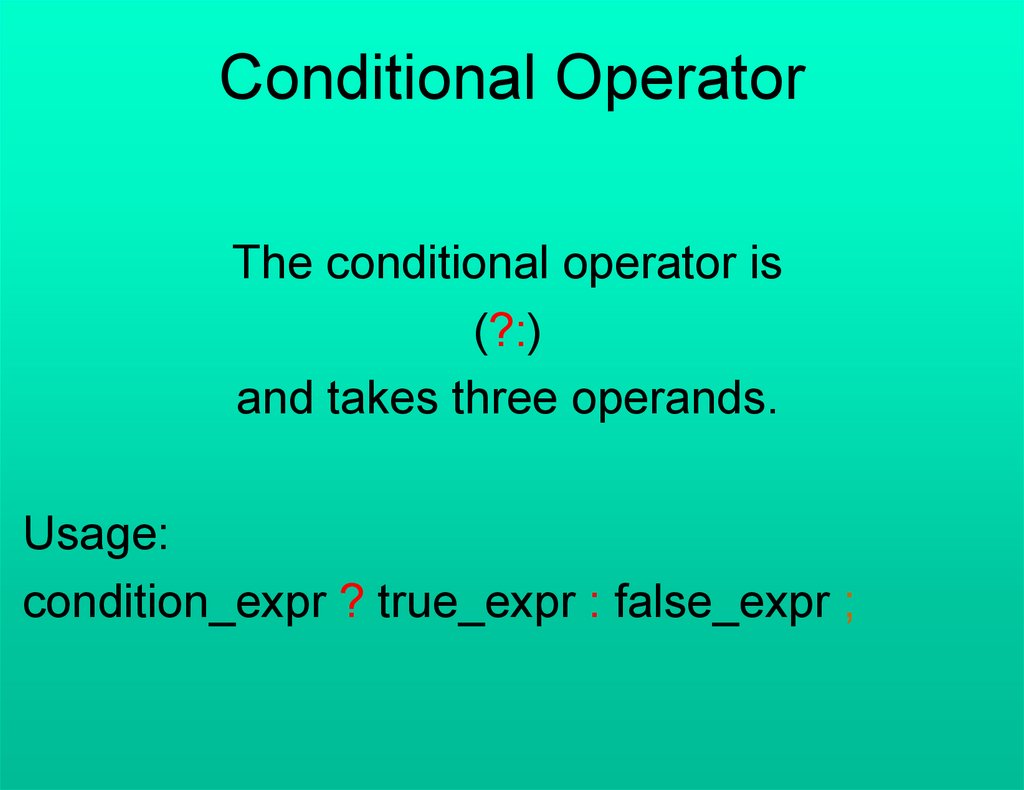
Conditional OperatorThe conditional operator is
(?:)
and takes three operands.
Usage:
condition_expr ? true_expr : false_expr ;
103.
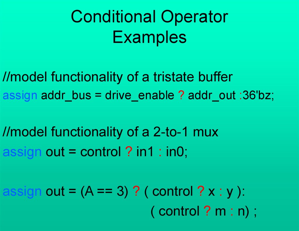
Conditional OperatorExamples
//model functionality of a tristate buffer
assign addr_bus = drive_enable ? addr_out :36'bz;
//model functionality of a 2-to-1 mux
assign out = control ? in1 : in0;
assign out = (A == 3) ? ( control ? x : y ):
( control ? m : n) ;
104.
BehavioralModeling
105.
Levels of description using verilogHDL
• Behavioral or algorithmic level
• Dataflow level
• Gate level
• Switch level
106.
Structured ProceduresThere are two structured procedure
statements in Verilog:
always
initial
107.
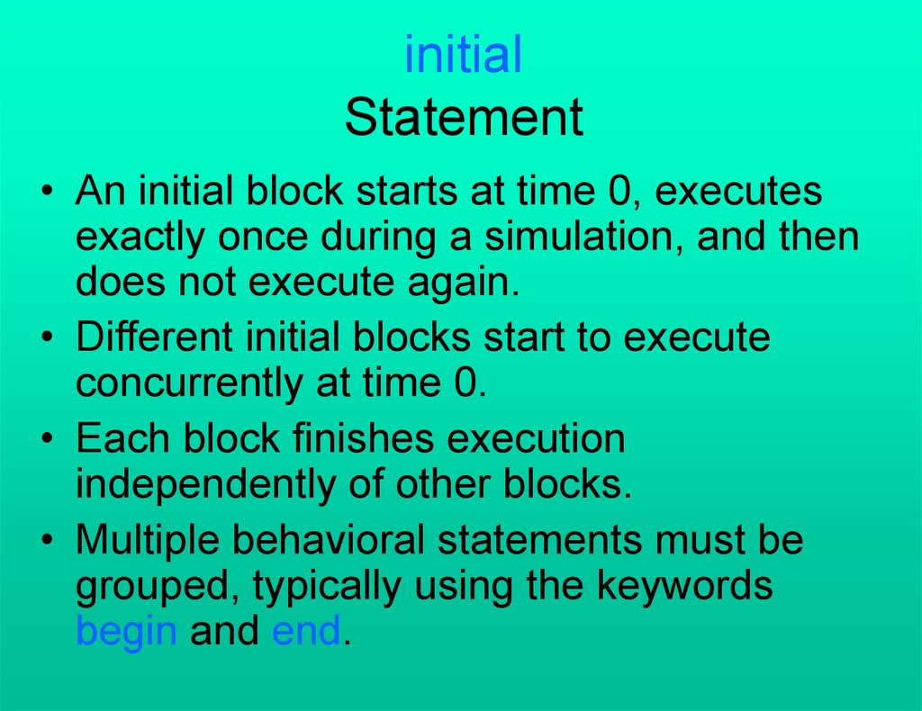
initialStatement
• An initial block starts at time 0, executes
exactly once during a simulation, and then
does not execute again.
• Different initial blocks start to execute
concurrently at time 0.
• Each block finishes execution
independently of other blocks.
• Multiple behavioral statements must be
grouped, typically using the keywords
begin and end.
108.
Examples of initial statementmodule stimulus;
reg x,y, a,b, m;
initial
m = 1'b0;
initial
begin
#5 a = 1'b1;
#25 b = 1'b0;
end
initial
begin
#10 x = 1'b0;
#25 y = 1'b1;
end
initial
#50 $finish;
endmodule
109.
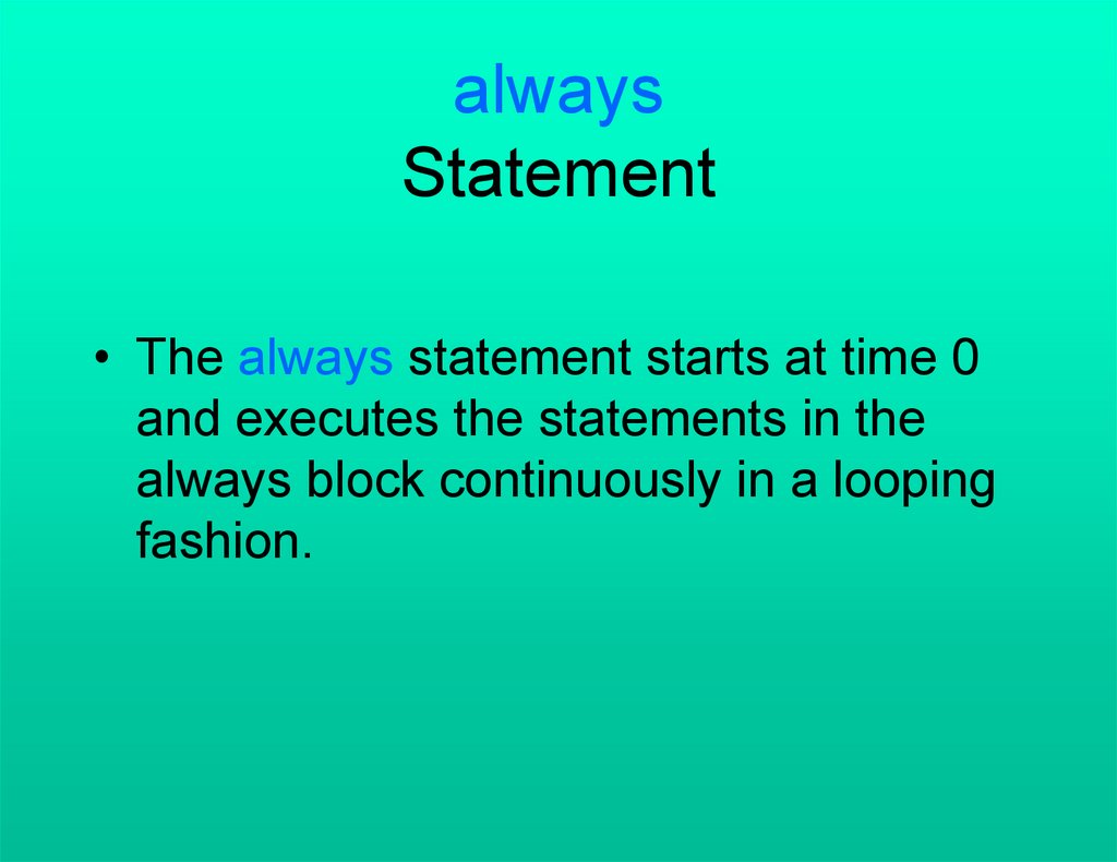
alwaysStatement
• The always statement starts at time 0
and executes the statements in the
always block continuously in a looping
fashion.
110.
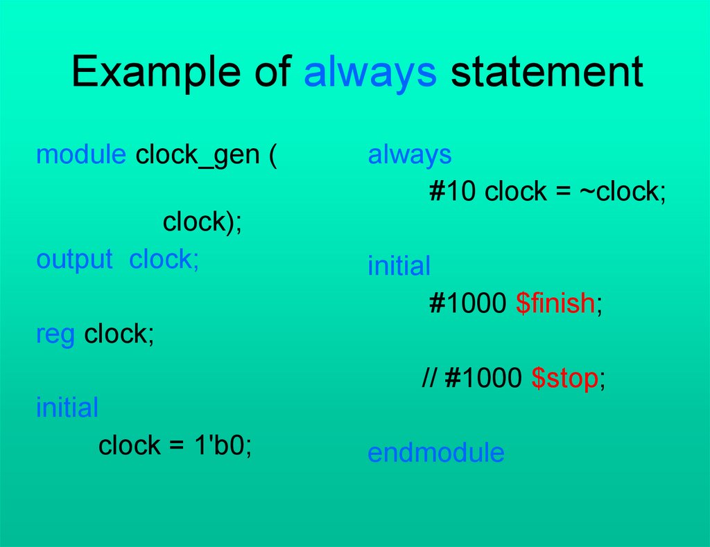
Example of always statementmodule clock_gen (
clock);
output clock;
always
#10 clock = ~clock;
initial
#1000 $finish;
reg clock;
// #1000 $stop;
initial
clock = 1'b0;
endmodule
111.
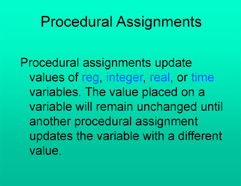
Procedural AssignmentsProcedural assignments update
values of reg, integer, real, or time
variables. The value placed on a
variable will remain unchanged until
another procedural assignment
updates the variable with a different
value.
112.
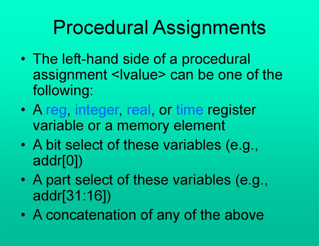
Procedural Assignments• The left-hand side of a procedural
assignment <lvalue> can be one of the
following:
• A reg, integer, real, or time register
variable or a memory element
• A bit select of these variables (e.g.,
addr[0])
• A part select of these variables (e.g.,
addr[31:16])
• A concatenation of any of the above
113.
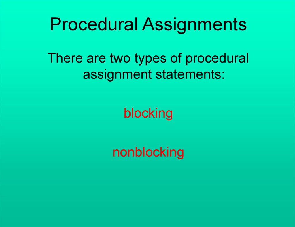
Procedural AssignmentsThere are two types of procedural
assignment statements:
blocking
nonblocking
114.
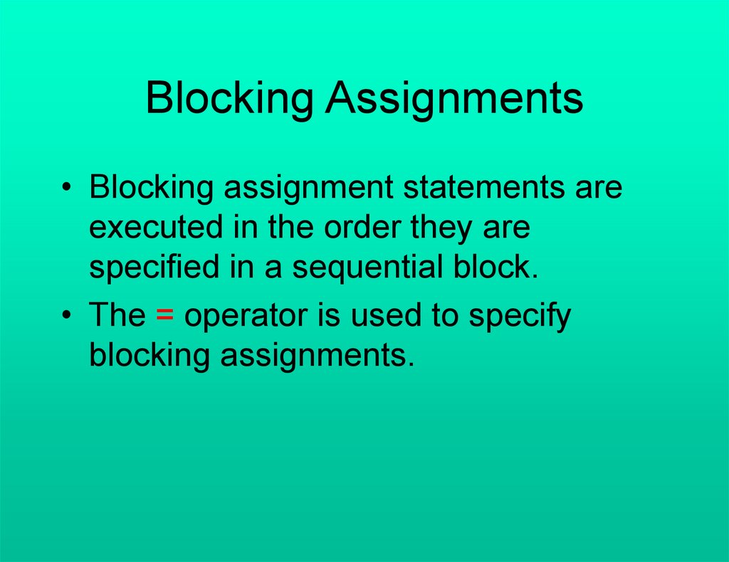
Blocking Assignments• Blocking assignment statements are
executed in the order they are
specified in a sequential block.
• The = operator is used to specify
blocking assignments.
115.
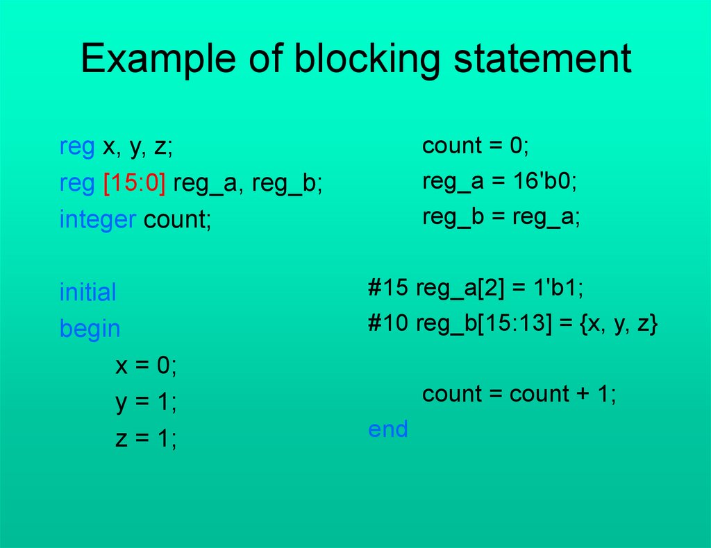
Example of blocking statementcount = 0;
reg_a = 16'b0;
reg_b = reg_a;
reg x, y, z;
reg [15:0] reg_a, reg_b;
integer count;
initial
begin
x = 0;
y = 1;
z = 1;
#15 reg_a[2] = 1'b1;
#10 reg_b[15:13] = {x, y, z}
count = count + 1;
end
116.
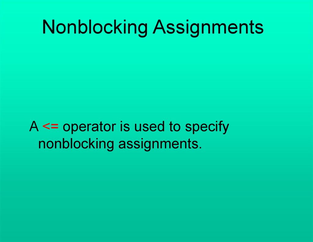
Nonblocking AssignmentsA <= operator is used to specify
nonblocking assignments.
117.
Nonblocking AssignmentsExample
reg x, y, z;
reg [15:0] reg_a, reg_b;
integer count;
initial
begin
x = 0;
y = 1;
z = 1;
count = 0;
reg_a = 16'b0;
reg_b = reg_a;
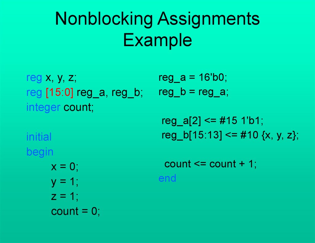
reg_a[2] <= #15 1'b1;
reg_b[15:13] <= #10 {x, y, z};
count <= count + 1;
end
118.
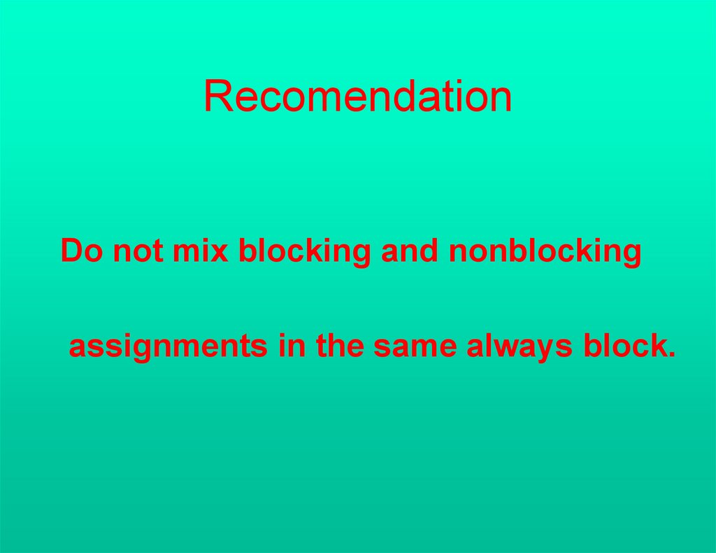
RecomendationDo not mix blocking and nonblocking
assignments in the same always block.
119.
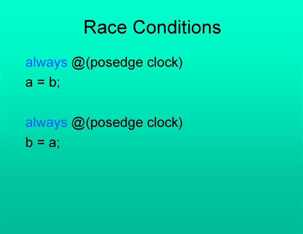
Race Conditionsalways @(posedge clock)
a = b;
always @(posedge clock)
b = a;
120.
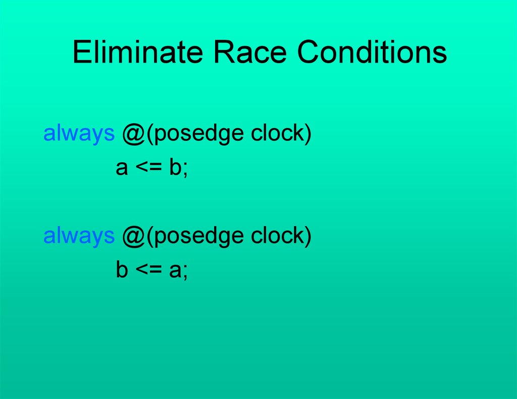
Eliminate Race Conditionsalways @(posedge clock)
a <= b;
always @(posedge clock)
b <= a;
121.
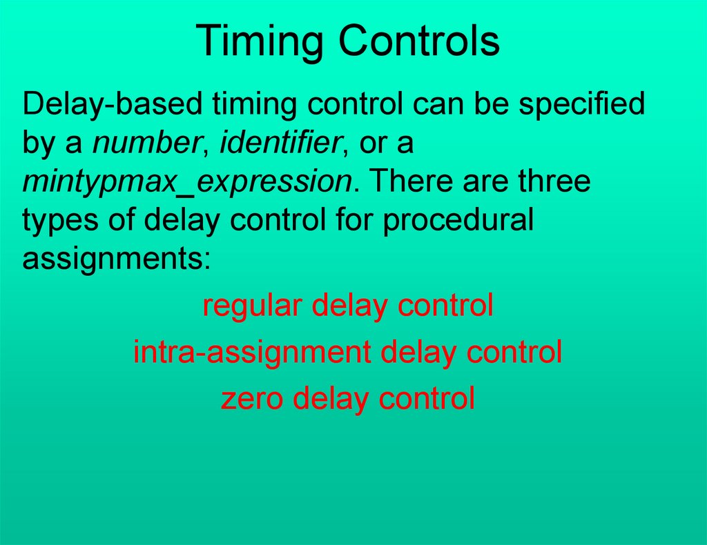
Timing ControlsDelay-based timing control can be specified
by a number, identifier, or a
mintypmax_expression. There are three
types of delay control for procedural
assignments:
regular delay control
intra-assignment delay control
zero delay control
122.
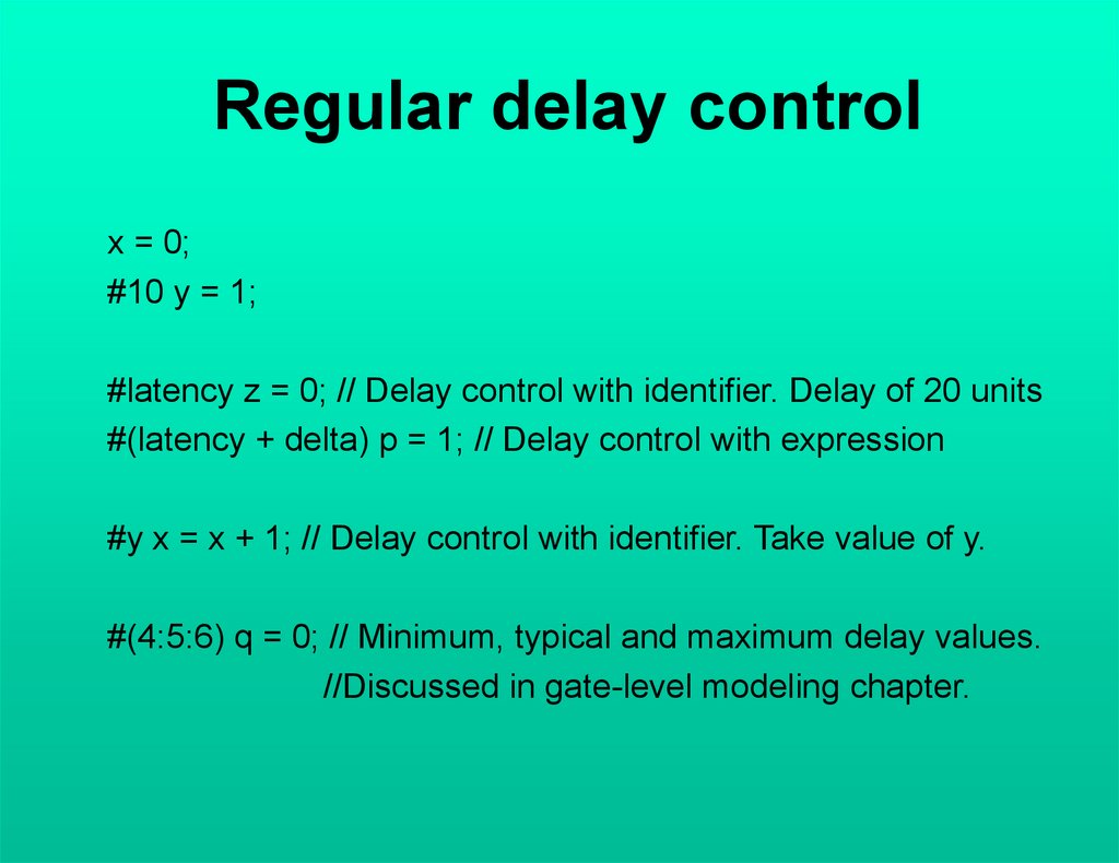
Regular delay controlx = 0;
#10 y = 1;
#latency z = 0; // Delay control with identifier. Delay of 20 units
#(latency + delta) p = 1; // Delay control with expression
#y x = x + 1; // Delay control with identifier. Take value of y.
#(4:5:6) q = 0; // Minimum, typical and maximum delay values.
//Discussed in gate-level modeling chapter.
123.
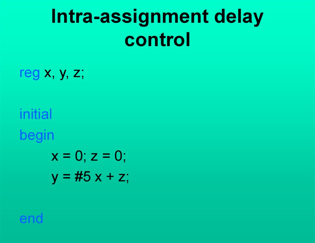
Intra-assignment delaycontrol
reg x, y, z;
initial
begin
x = 0; z = 0;
y = #5 x + z;
end
124.
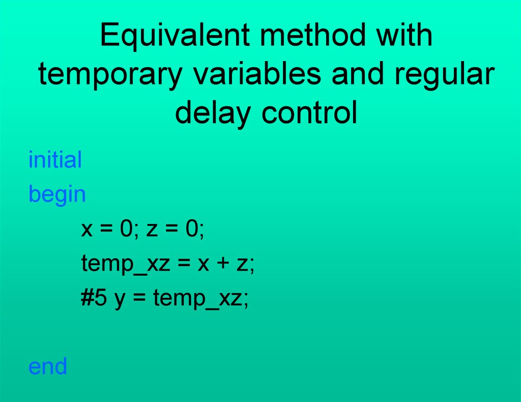
Equivalent method withtemporary variables and regular
delay control
initial
begin
x = 0; z = 0;
temp_xz = x + z;
#5 y = temp_xz;
end
125.
Zero delay controlinitial
begin
x = 0;
y = 0;
end
initial
begin
#0 x = 1; //zero delay control
#0 y = 1;
end
126.
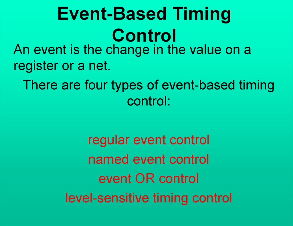
Event-Based TimingControl
An event is the change in the value on a
register or a net.
There are four types of event-based timing
control:
regular event control
named event control
event OR control
level-sensitive timing control
127.
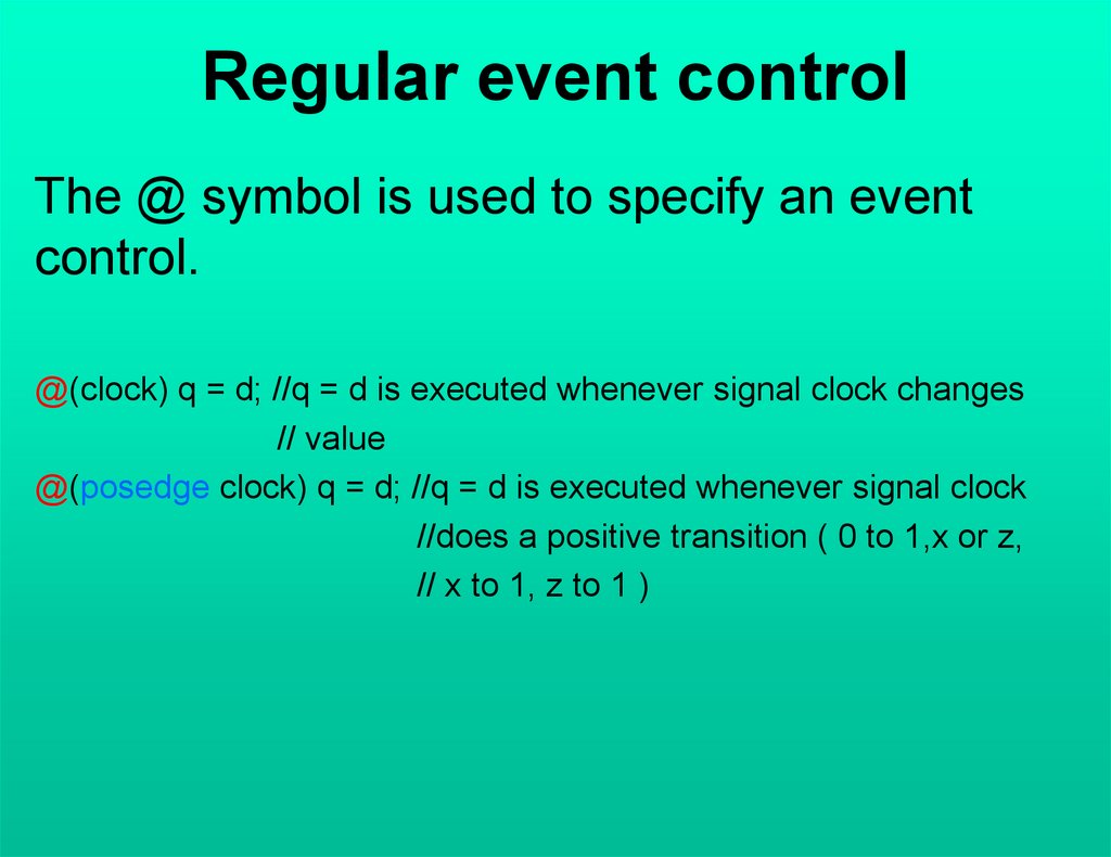
Regular event controlThe @ symbol is used to specify an event
control.
@(clock) q = d; //q = d is executed whenever signal clock changes
// value
@(posedge clock) q = d; //q = d is executed whenever signal clock
//does a positive transition ( 0 to 1,x or z,
// x to 1, z to 1 )
128.
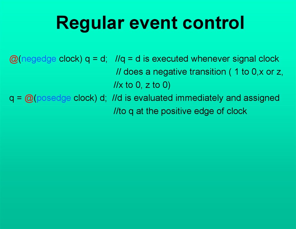
Regular event control@(negedge clock) q = d; //q = d is executed whenever signal clock
// does a negative transition ( 1 to 0,x or z,
//x to 0, z to 0)
q = @(posedge clock) d; //d is evaluated immediately and assigned
//to q at the positive edge of clock
129.
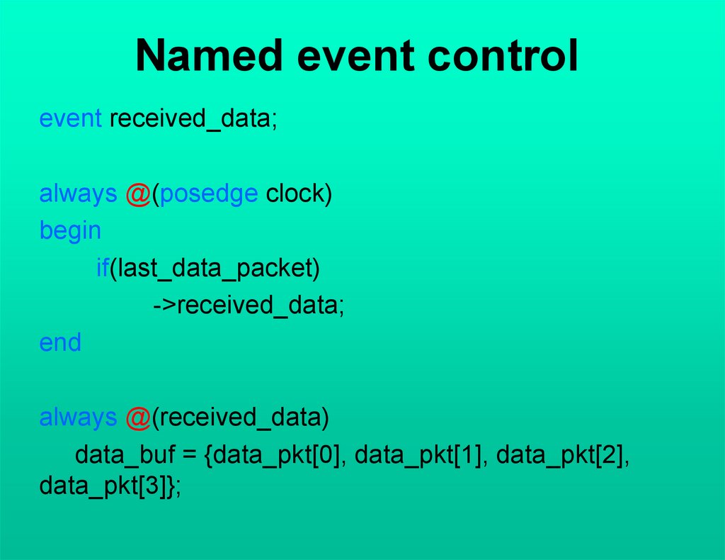
Named event controlevent received_data;
always @(posedge clock)
begin
if(last_data_packet)
->received_data;
end
always @(received_data)
data_buf = {data_pkt[0], data_pkt[1], data_pkt[2],
data_pkt[3]};
130.
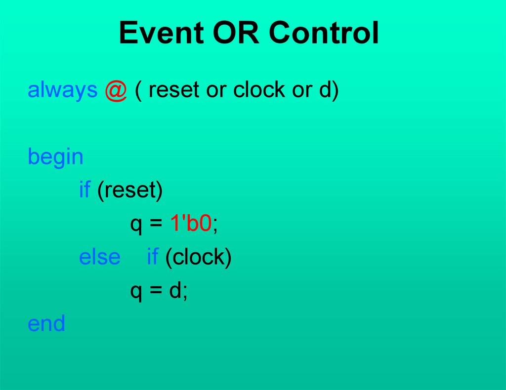
Event OR Controlalways @ ( reset or clock or d)
begin
if (reset)
q = 1'b0;
else if (clock)
q = d;
end
131.
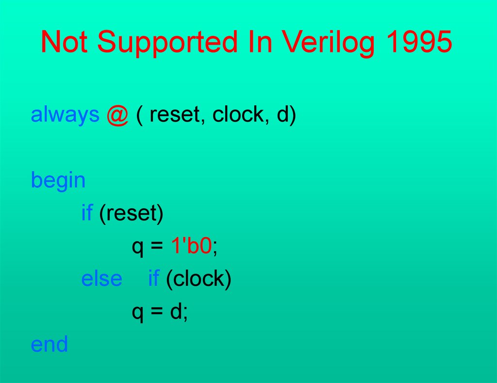
Not Supported In Verilog 1995always @ ( reset, clock, d)
begin
if (reset)
q = 1'b0;
else if (clock)
q = d;
end
132.
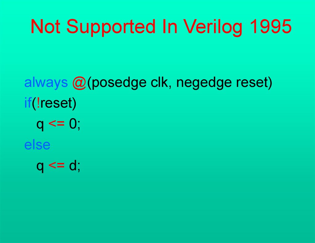
Not Supported In Verilog 1995always @(posedge clk, negedge reset)
if(!reset)
q <= 0;
else
q <= d;
133.
Suppored by Verilog 1995always @(a or b or c or d or e or f or g or h or p or m)
begin
out1 = a ? b+c : d+e;
out2 = f ? g+h : p+m;
end
134.
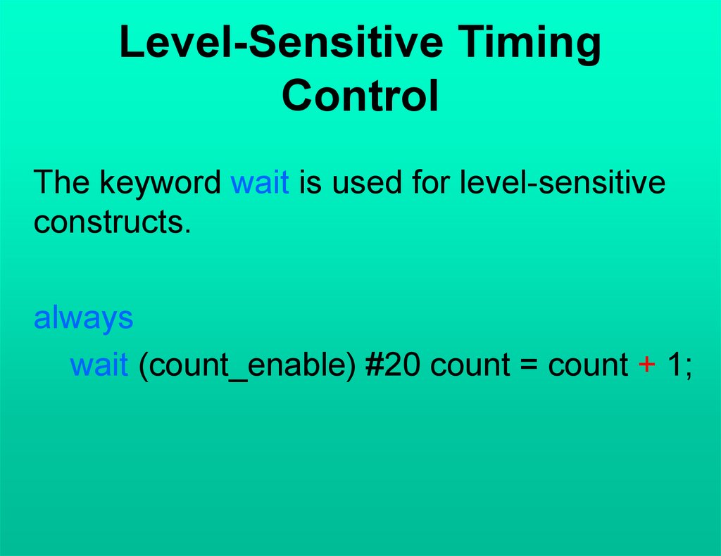
Level-Sensitive TimingControl
The keyword wait is used for level-sensitive
constructs.
always
wait (count_enable) #20 count = count + 1;
135.
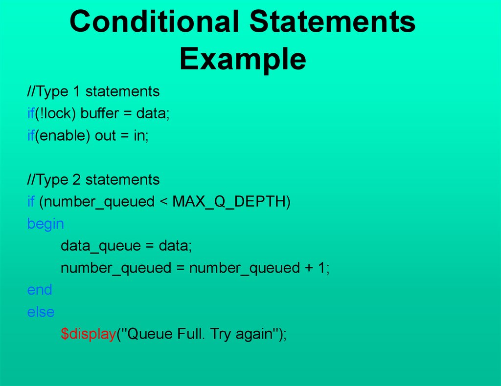
Conditional StatementsExample
//Type 1 statements
if(!lock) buffer = data;
if(enable) out = in;
//Type 2 statements
if (number_queued < MAX_Q_DEPTH)
begin
data_queue = data;
number_queued = number_queued + 1;
end
else
$display("Queue Full. Try again");
136.
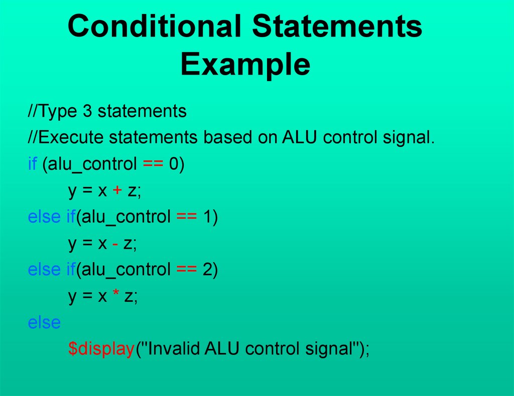
Conditional StatementsExample
//Type 3 statements
//Execute statements based on ALU control signal.
if (alu_control == 0)
y = x + z;
else if(alu_control == 1)
y = x - z;
else if(alu_control == 2)
y = x * z;
else
$display("Invalid ALU control signal");
137.
Multiway BranchingThe keywords case, endcase, and default are
used in the case statement.
case (expression)
alternative1: statement1;
alternative2: statement2;
alternative3: statement3;
...
...
default: default_statement;
endcase
138.
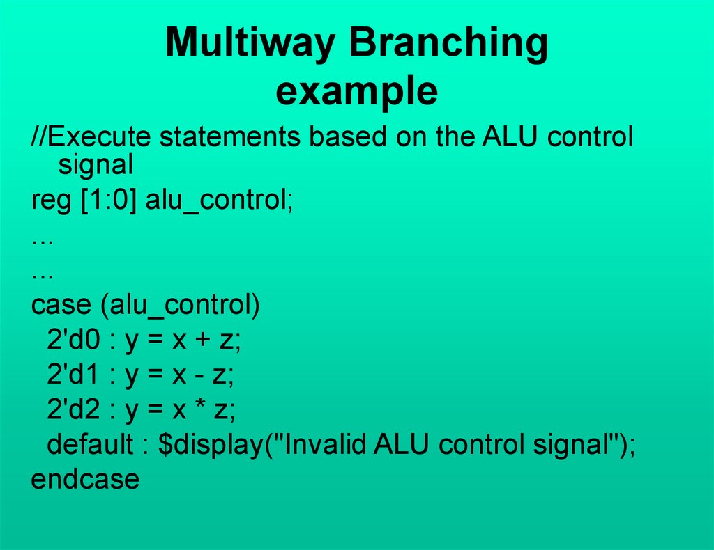
Multiway Branchingexample
//Execute statements based on the ALU control
signal
reg [1:0] alu_control;
...
...
case (alu_control)
2'd0 : y = x + z;
2'd1 : y = x - z;
2'd2 : y = x * z;
default : $display("Invalid ALU control signal");
endcase
139.
Multiway Branchingexample
module mux4_to_1 (out, i0, i1, i2, i3, s1, s0);
output out;
input i0, i1, i2, i3;
input s1, s0;
reg out;
always @ (s1 or s0 or i0 or i1 or i2 or i3)
case ({s1, s0})
2'd0 : out = i0;
2'd1 : out = i1;
2'd2 : out = i2;
2'd3 : out = i3;
default: $display("Invalid control signals");
endcase
endmodule
140.
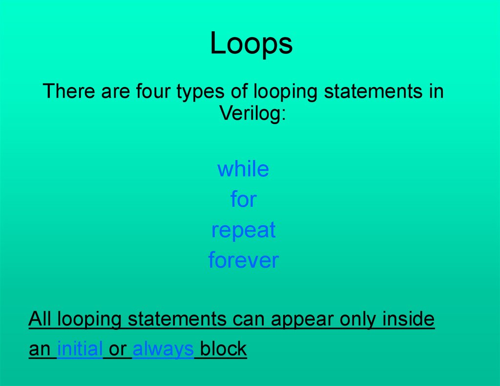
LoopsThere are four types of looping statements in
Verilog:
while
for
repeat
forever
All looping statements can appear only inside
an initial or always block
141.
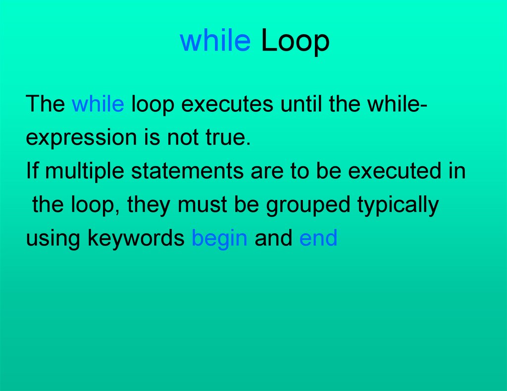
while LoopThe while loop executes until the whileexpression is not true.
If multiple statements are to be executed in
the loop, they must be grouped typically
using keywords begin and end
142.
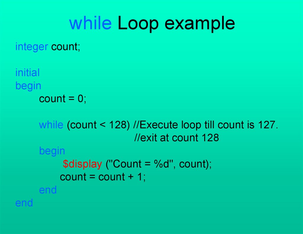
while Loop exampleinteger count;
initial
begin
count = 0;
while (count < 128) //Execute loop till count is 127.
//exit at count 128
begin
$display ("Count = %d", count);
count = count + 1;
end
end
143.
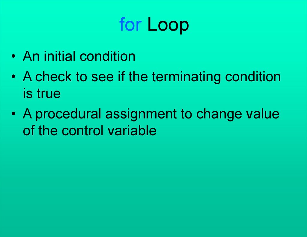
for Loop• An initial condition
• A check to see if the terminating condition
is true
• A procedural assignment to change value
of the control variable
144.
for Loop Exampleinteger count;
initial
for ( count=0; count < 128; count = count + 1)
$display ("Count = %d", count);
145.
repeat LoopThe keyword repeat is used for this loop.
integer count;
initial
begin
count = 0;
repeat(128)
begin
$display("Count = %d", count);
count = count + 1;
end
end
146.
forever loopThe keyword forever is used to express this
Loop. The loop does not contain any
expression and executes forever until the
$finish task is encountered.
147.
forever loop examplereg clock;
initial
begin
clock = 1'b0;
forever #10 clock = ~clock;
end
148.
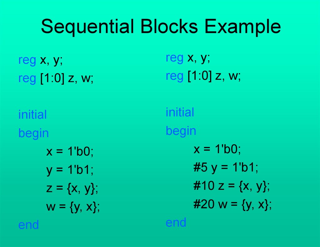
Sequential and Parallel BlocksThe keywords begin and end are used to
group statements into sequential blocks.
Sequential blocks have the following
characteristics:
149.
Sequential Blocks Examplereg x, y;
reg [1:0] z, w;
reg x, y;
reg [1:0] z, w;
initial
begin
x = 1'b0;
y = 1'b1;
z = {x, y};
w = {y, x};
end
initial
begin
x = 1'b0;
#5 y = 1'b1;
#10 z = {x, y};
#20 w = {y, x};
end
150.
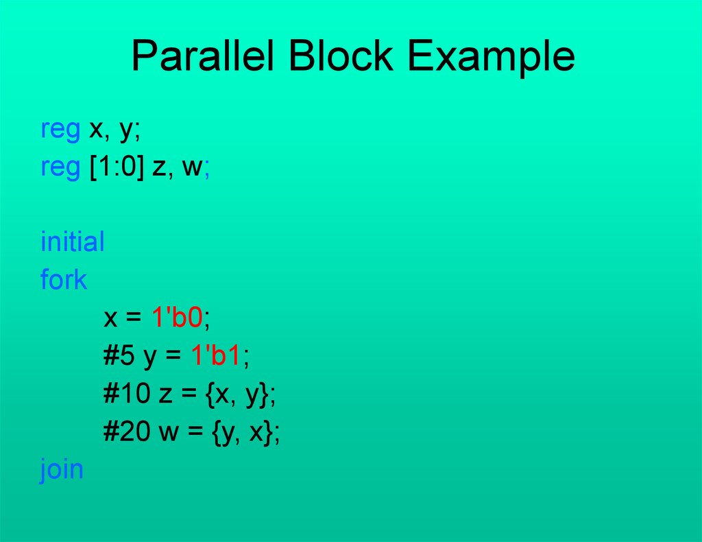
Parallel Block Examplereg x, y;
reg [1:0] z, w;
initial
fork
x = 1'b0;
#5 y = 1'b1;
#10 z = {x, y};
#20 w = {y, x};
join
151.
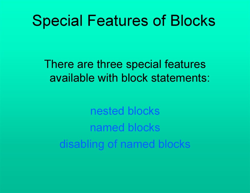
Special Features of BlocksThere are three special features
available with block statements:
nested blocks
named blocks
disabling of named blocks
152.
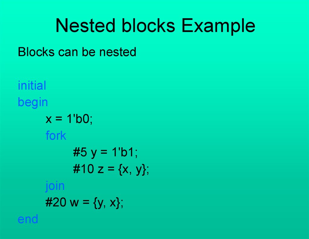
Nested blocks ExampleBlocks can be nested
initial
begin
x = 1'b0;
fork
#5 y = 1'b1;
#10 z = {x, y};
join
#20 w = {y, x};
end
153.
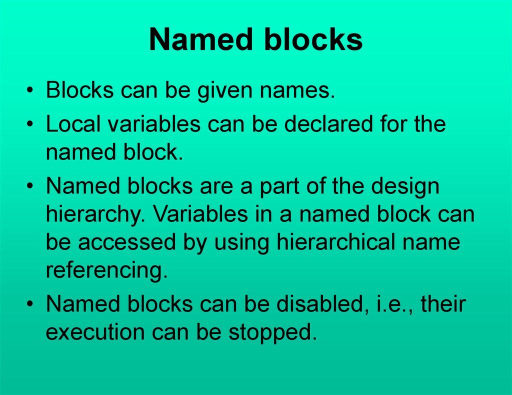
Named blocks• Blocks can be given names.
• Local variables can be declared for the
named block.
• Named blocks are a part of the design
hierarchy. Variables in a named block can
be accessed by using hierarchical name
referencing.
• Named blocks can be disabled, i.e., their
execution can be stopped.
154.
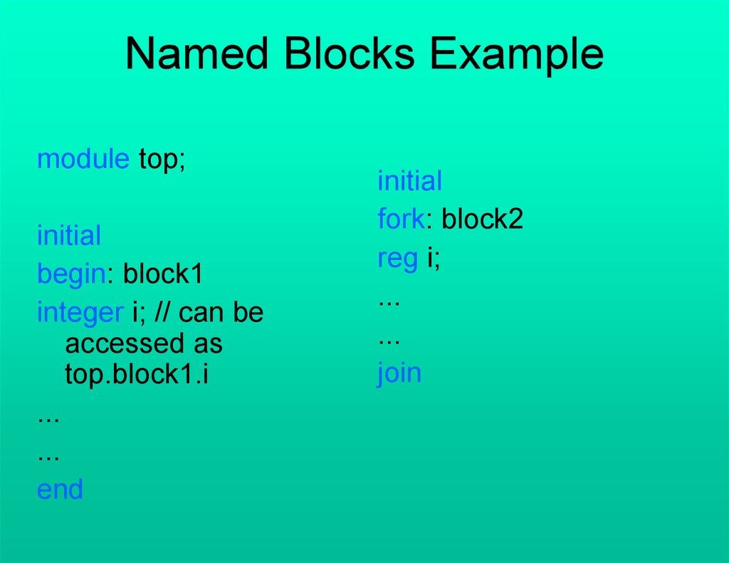
Named Blocks Examplemodule top;
initial
begin: block1
integer i; // can be
accessed as
top.block1.i
...
...
end
initial
fork: block2
reg i;
...
...
join
155.
Disabling named blocksThe keyword disable provides a way to
terminate the execution of a named block.
156.
Timing and Delays157.
Types of Delay ModelsThere are three types of delay models
used in Verilog:
Distributed
Lumped
Pin-to-pin (path)
delays.
158.
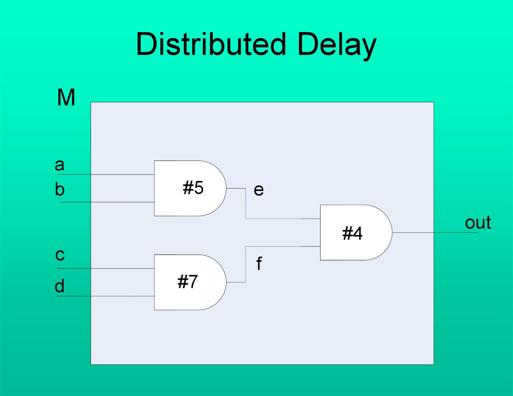
Distributed DelayM
a
b
#5
e
#4
c
d
f
#7
out
159.
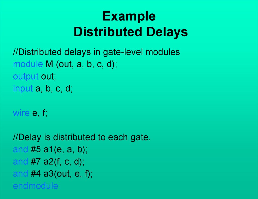
ExampleDistributed Delays
//Distributed delays in gate-level modules
module M (out, a, b, c, d);
output out;
input a, b, c, d;
wire e, f;
//Delay is distributed to each gate.
and #5 a1(e, a, b);
and #7 a2(f, c, d);
and #4 a3(out, e, f);
endmodule
160.
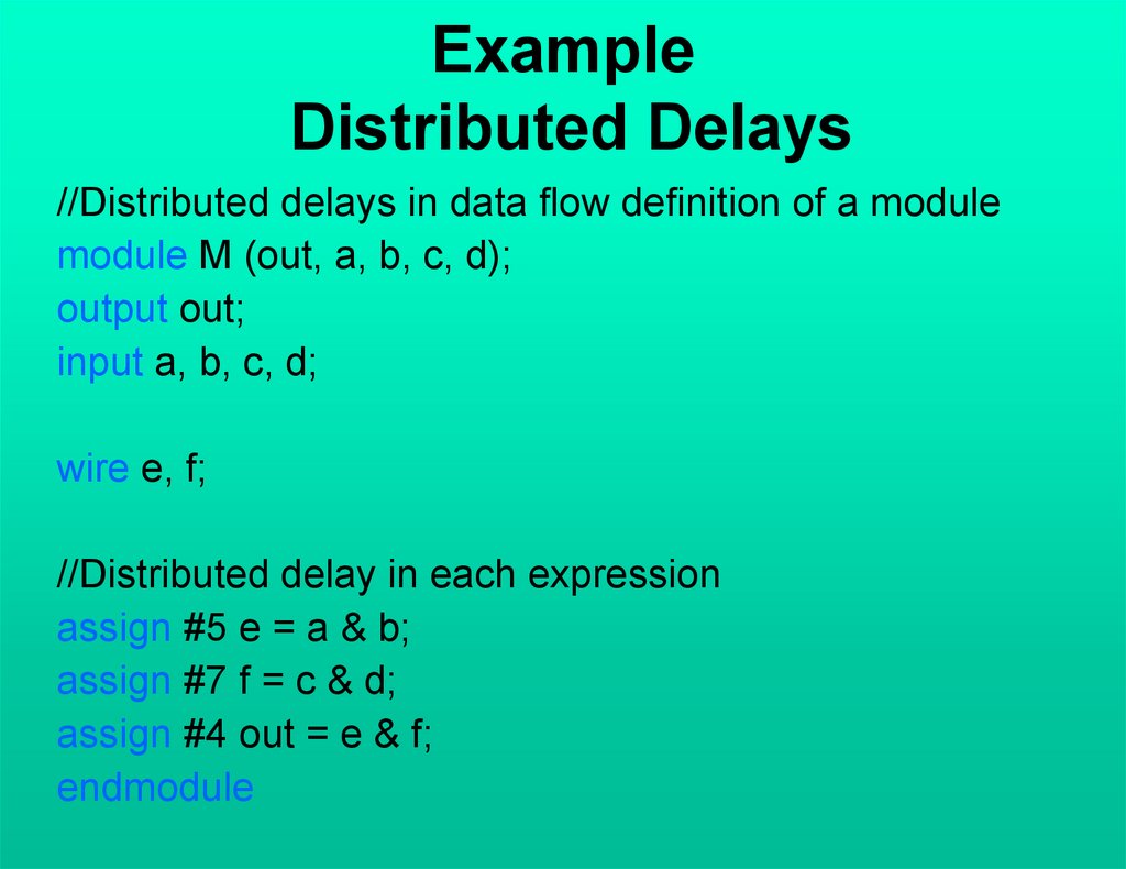
ExampleDistributed Delays
//Distributed delays in data flow definition of a module
module M (out, a, b, c, d);
output out;
input a, b, c, d;
wire e, f;
//Distributed delay in each expression
assign #5 e = a & b;
assign #7 f = c & d;
assign #4 out = e & f;
endmodule
161.
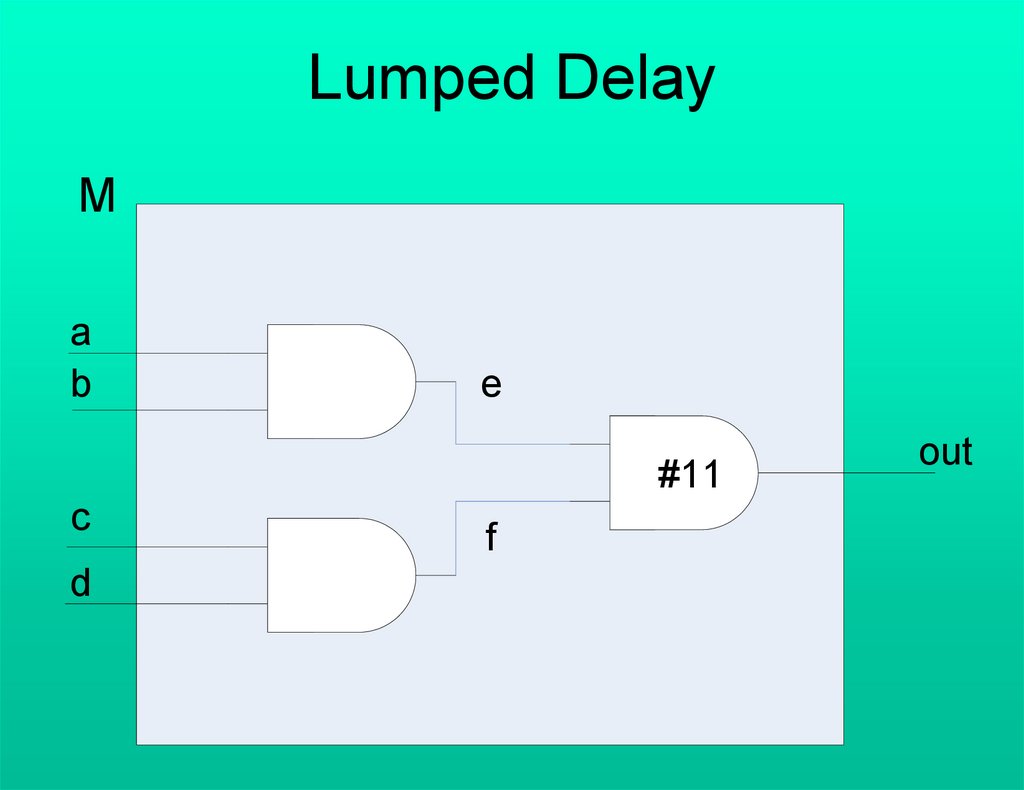
Lumped DelayM
a
b
e
#11
c
d
f
out
162.
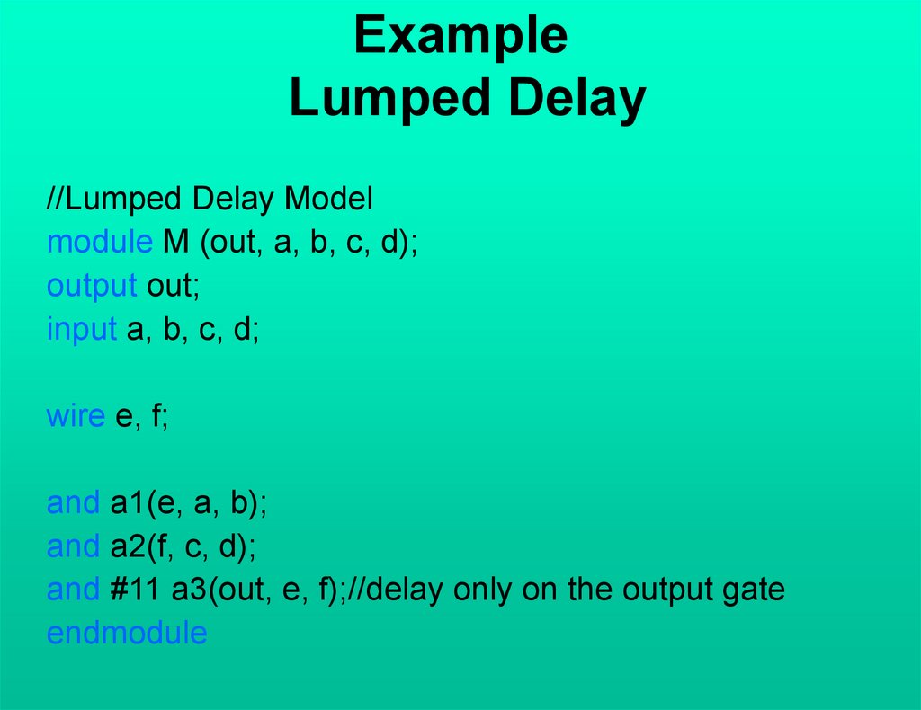
ExampleLumped Delay
//Lumped Delay Model
module M (out, a, b, c, d);
output out;
input a, b, c, d;
wire e, f;
and a1(e, a, b);
and a2(f, c, d);
and #11 a3(out, e, f);//delay only on the output gate
endmodule
163.
Pin-to-Pin DelaysM
a
b
e
out
c
f
d
Path a-e-out delay = 9 Path c-f-out delay = 11
Path b-e-out delay = 9 Path d-f-out delay = 11
164.
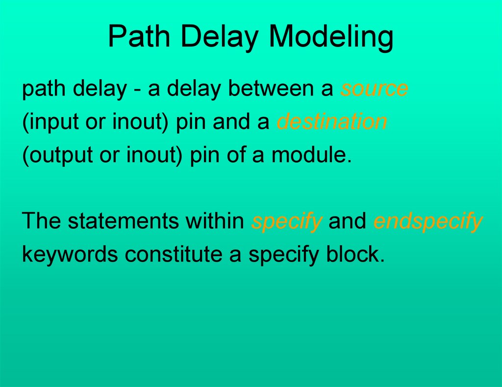
Path Delay Modelingpath delay - a delay between a source
(input or inout) pin and a destination
(output or inout) pin of a module.
The statements within specify and endspecify
keywords constitute a specify block.
165.
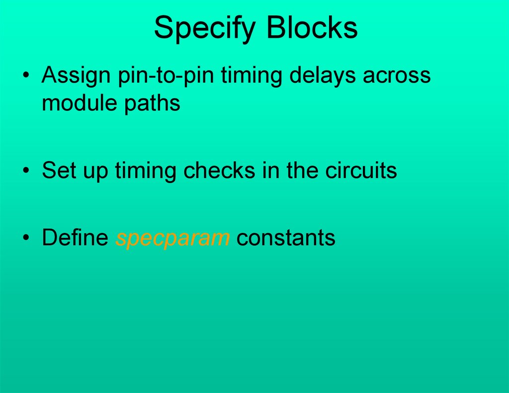
Specify Blocks• Assign pin-to-pin timing delays across
module paths
• Set up timing checks in the circuits
• Define specparam constants
166.
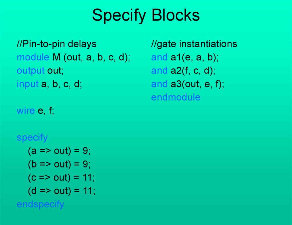
Specify Blocks//Pin-to-pin delays
module M (out, a, b, c, d);
output out;
input a, b, c, d;
wire e, f;
specify
(a => out) = 9;
(b => out) = 9;
(c => out) = 11;
(d => out) = 11;
endspecify
//gate instantiations
and a1(e, a, b);
and a2(f, c, d);
and a3(out, e, f);
endmodule
167.
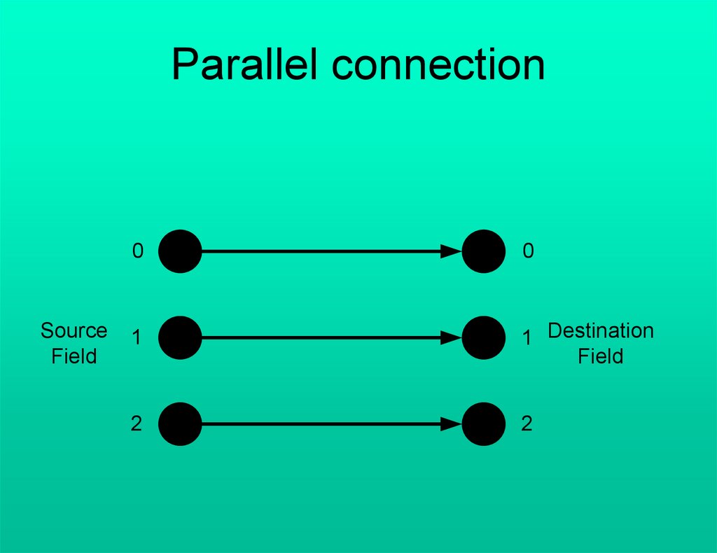
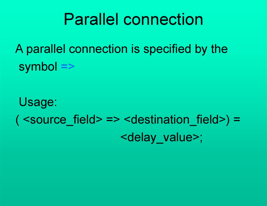
Parallel connectionA parallel connection is specified by the
symbol =>
Usage:
( <source_field> => <destination_field>) =
<delay_value>;
168.
Parallel connectionSource
Field
0
0
1
1 Destination
Field
2
2
169.
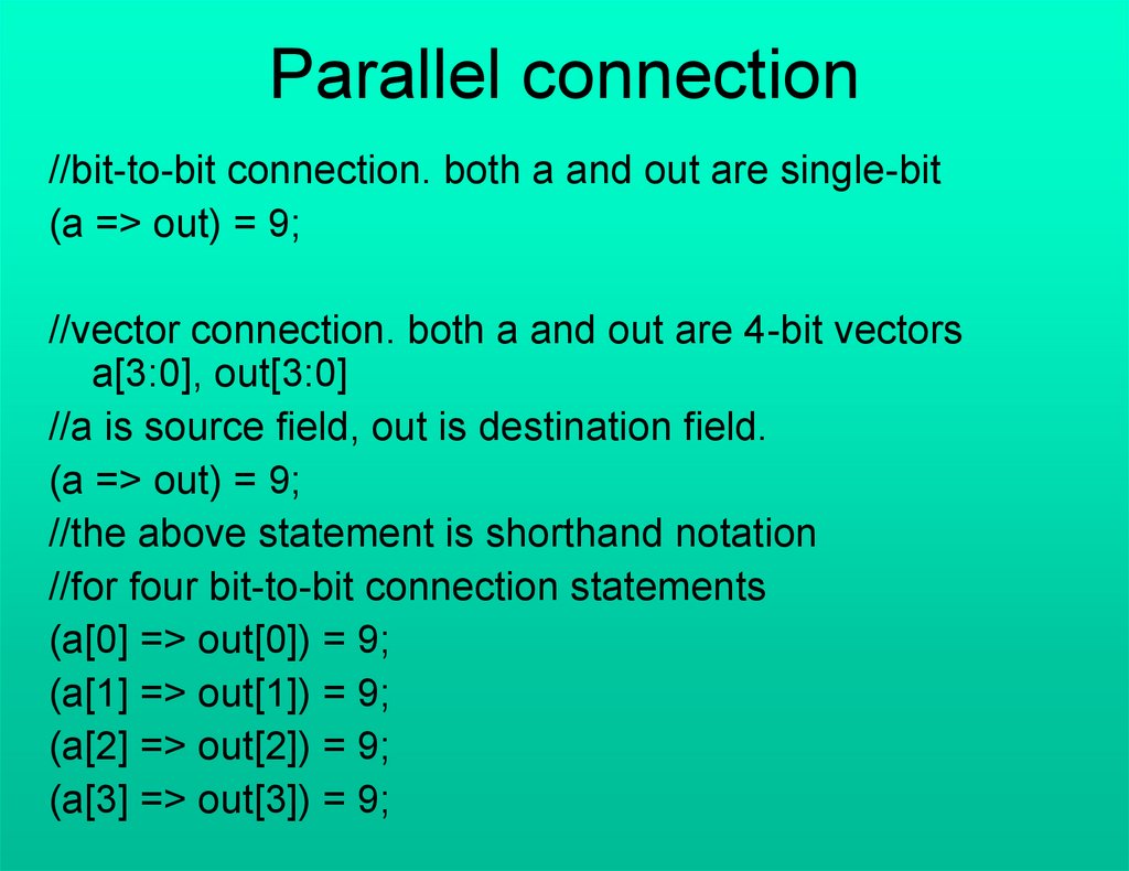
Parallel connection//bit-to-bit connection. both a and out are single-bit
(a => out) = 9;
//vector connection. both a and out are 4-bit vectors
a[3:0], out[3:0]
//a is source field, out is destination field.
(a => out) = 9;
//the above statement is shorthand notation
//for four bit-to-bit connection statements
(a[0] => out[0]) = 9;
(a[1] => out[1]) = 9;
(a[2] => out[2]) = 9;
(a[3] => out[3]) = 9;
170.
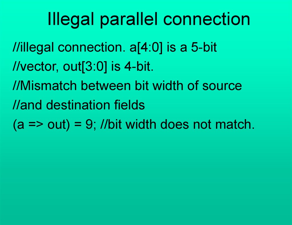
Illegal parallel connection//illegal connection. a[4:0] is a 5-bit
//vector, out[3:0] is 4-bit.
//Mismatch between bit width of source
//and destination fields
(a => out) = 9; //bit width does not match.
171.
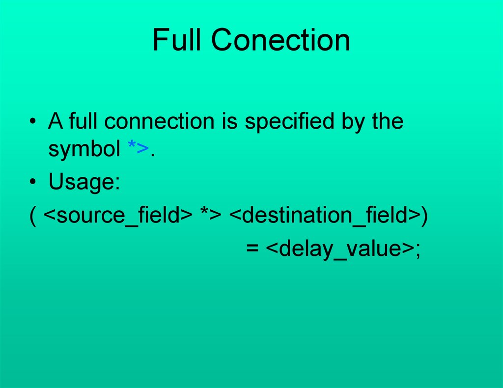
Full Conection• A full connection is specified by the
symbol *>.
• Usage:
( <source_field> *> <destination_field>)
= <delay_value>;
172.
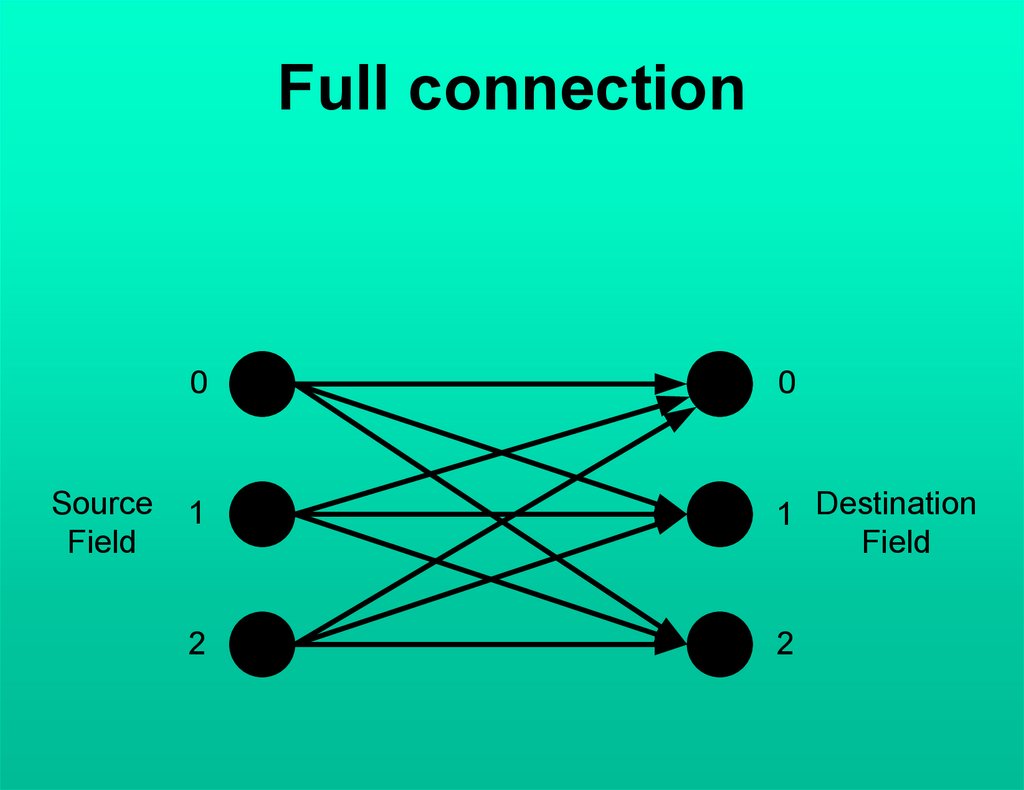
Full connectionSource
Field
0
0
1
1 Destination
Field
2
2
173.
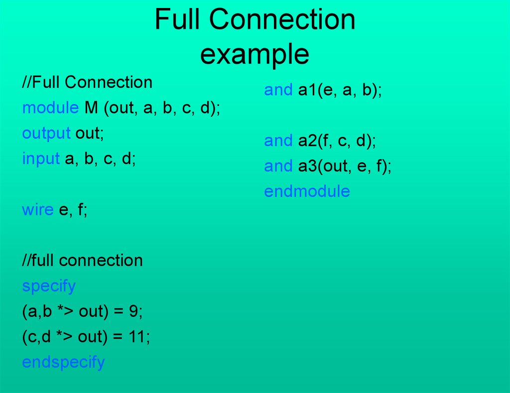
Full Connectionexample
//Full Connection
module M (out, a, b, c, d);
output out;
input a, b, c, d;
wire e, f;
//full connection
specify
(a,b *> out) = 9;
(c,d *> out) = 11;
endspecify
and a1(e, a, b);
and a2(f, c, d);
and a3(out, e, f);
endmodule
174.
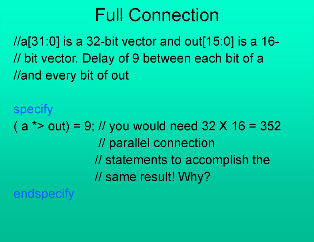
Full Connection//a[31:0] is a 32-bit vector and out[15:0] is a 16// bit vector. Delay of 9 between each bit of a
//and every bit of out
specify
( a *> out) = 9; // you would need 32 X 16 = 352
// parallel connection
// statements to accomplish the
// same result! Why?
endspecify
175.
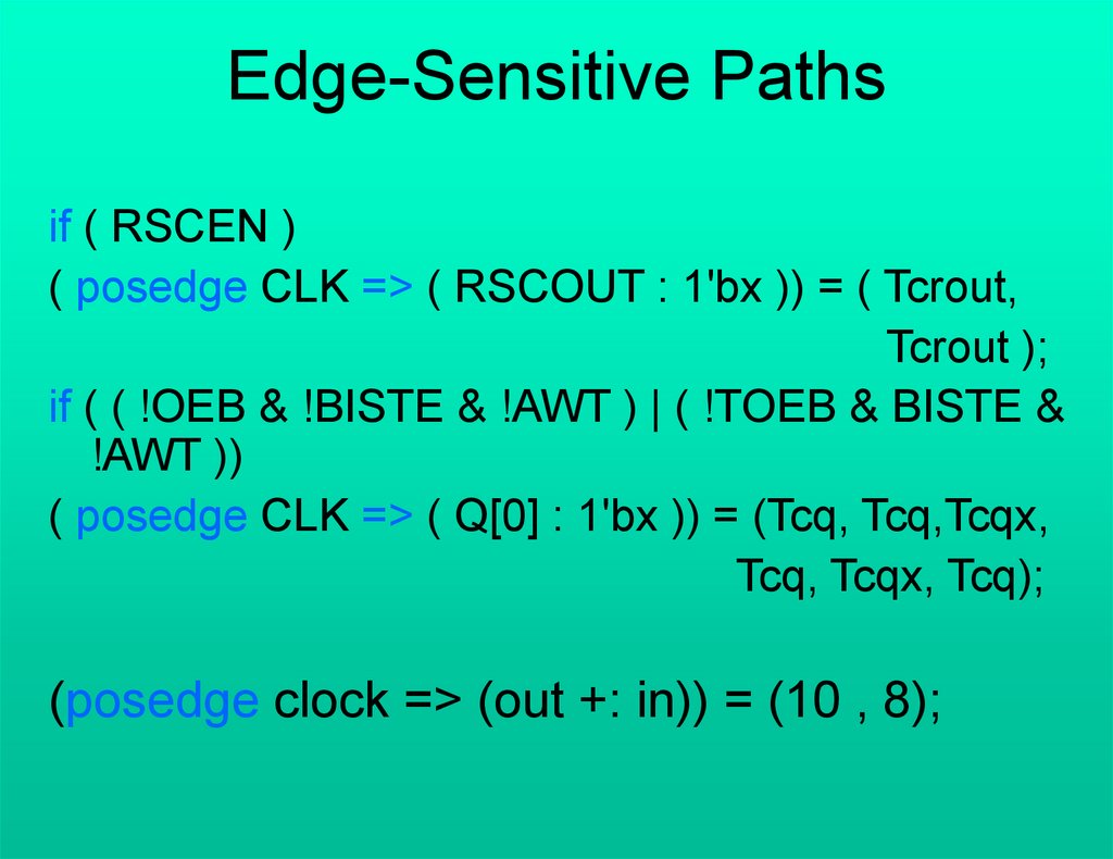
Edge-Sensitive Pathsif ( RSCEN )
( posedge CLK => ( RSCOUT : 1'bx )) = ( Tcrout,
Tcrout );
if ( ( !OEB & !BISTE & !AWT ) | ( !TOEB & BISTE &
!AWT ))
( posedge CLK => ( Q[0] : 1'bx )) = (Tcq, Tcq,Tcqx,
Tcq, Tcqx, Tcq);
(posedge clock => (out +: in)) = (10 , 8);
176.
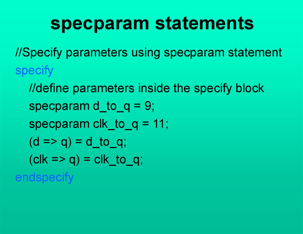
specparam statements//Specify parameters using specparam statement
specify
//define parameters inside the specify block
specparam d_to_q = 9;
specparam clk_to_q = 11;
(d => q) = d_to_q;
(clk => q) = clk_to_q;
endspecify
177.
Conditional path delaysspecify
if (a) (a => out) = 9;
if (~a) (a => out) = 10;
if (b & c) (b => out) = 9;
if (~(b & c)) (b => out) = 13;
if ({c,d} == 2'b01)
(c,d *> out) = 11;
if ({c,d} != 2'b01)
(c,d *> out) = 13;
endspecify
178.
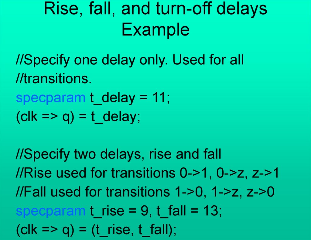
Rise, fall, and turn-off delaysOne, two, three, six, or twelve delay
values can be specified for any path.
Four, five, seven, eight, nine, ten, or
eleven delay value specification is illegal.
179.
Rise, fall, and turn-off delaysExample
//Specify one delay only. Used for all
//transitions.
specparam t_delay = 11;
(clk => q) = t_delay;
//Specify two delays, rise and fall
//Rise used for transitions 0->1, 0->z, z->1
//Fall used for transitions 1->0, 1->z, z->0
specparam t_rise = 9, t_fall = 13;
(clk => q) = (t_rise, t_fall);
180.
Rise, fall, and turn-off delaysExample
//Specify three delays, rise, fall, and turn-off
//Rise used for transitions 0->1, z->1
//Fall used for transitions 1->0, z->0
//Turn-off used for transitions 0->z, 1->z
specparam t_rise = 9, t_fall = 13, t_turnoff
= 11;
(clk => q) = (t_rise, t_fall, t_turnoff);
181.
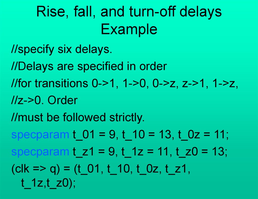
Rise, fall, and turn-off delaysExample
//specify six delays.
//Delays are specified in order
//for transitions 0->1, 1->0, 0->z, z->1, 1->z,
//z->0. Order
//must be followed strictly.
specparam t_01 = 9, t_10 = 13, t_0z = 11;
specparam t_z1 = 9, t_1z = 11, t_z0 = 13;
(clk => q) = (t_01, t_10, t_0z, t_z1,
t_1z,t_z0);
182.
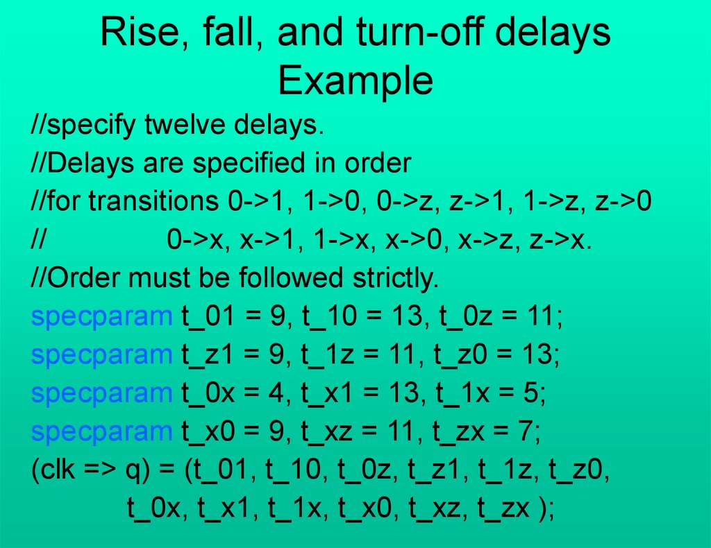
Rise, fall, and turn-off delaysExample
//specify twelve delays.
//Delays are specified in order
//for transitions 0->1, 1->0, 0->z, z->1, 1->z, z->0
//
0->x, x->1, 1->x, x->0, x->z, z->x.
//Order must be followed strictly.
specparam t_01 = 9, t_10 = 13, t_0z = 11;
specparam t_z1 = 9, t_1z = 11, t_z0 = 13;
specparam t_0x = 4, t_x1 = 13, t_1x = 5;
specparam t_x0 = 9, t_xz = 11, t_zx = 7;
(clk => q) = (t_01, t_10, t_0z, t_z1, t_1z, t_z0,
t_0x, t_x1, t_1x, t_x0, t_xz, t_zx );
183.
Min, max, and typicaldelays
//Specify three delays, rise, fall, and turn-off
//Each delay has a min:typ:max value
specparam t_rise = 8:9:10, t_fall = 12:13:14,
t_turnoff = 10:11:12;
(clk => q) = (t_rise, t_fall, t_turnoff);
+mindelays, +typdelays, +maxdelays
184.
Handling x transitions• Transitions from x to a known state
should take the maximum possible
time
• Transition from a known state to x
should take the minimum possible time
185.
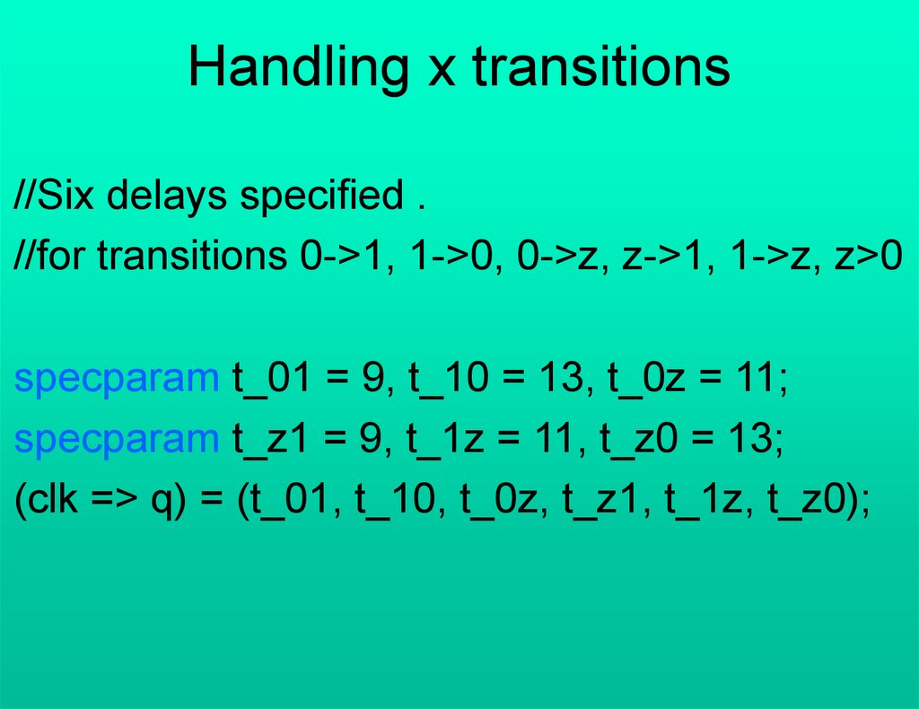
Handling x transitions//Six delays specified .
//for transitions 0->1, 1->0, 0->z, z->1, 1->z, z>0
specparam t_01 = 9, t_10 = 13, t_0z = 11;
specparam t_z1 = 9, t_1z = 11, t_z0 = 13;
(clk => q) = (t_01, t_10, t_0z, t_z1, t_1z, t_z0);
186.
Handling x transitions0->x min(t_01, t_0z) = 9
x->0 max(t_10, t_z0) = 13
1->x min(t_10, t_1z) = 11
x->1 max(t_01, t_z1) = 9
z->x min(t_z0, t_z1) = 9
x->z max(t_1z, t_0z) = 11
187.
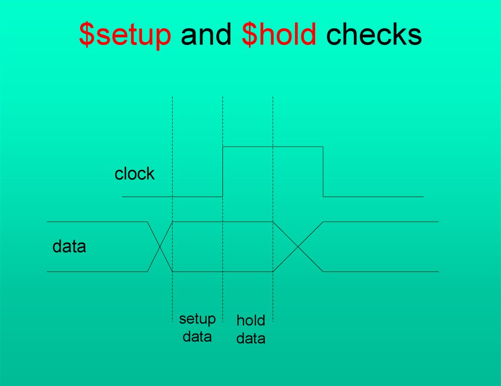
Timing Checks$setup and $hold checks
• the setup time is the minimum time the
data must arrive before the active clock
edge.
• The hold time is the minimum time the
data cannot change after the active
clock edge.
188.
$setup and $hold checksclock
data
setup
data
hold
data
189.
$setup taskUsage:
$setup(data_event, reference_event, limit);
data_event : Signal that is monitored for violations
reference_event : Signal that establishes a
reference for monitoring the data_event signal
Limit : Minimum time required for setup of data
event
190.
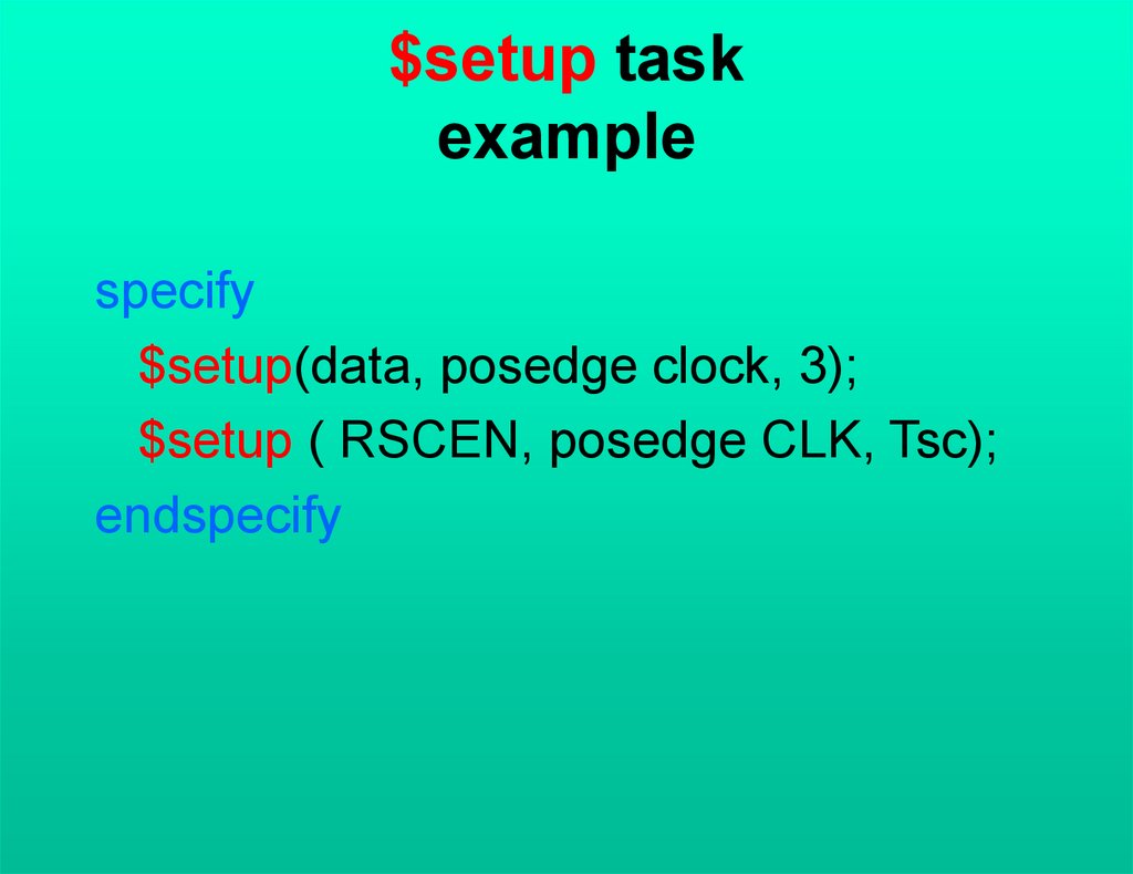
$setup taskexample
specify
$setup(data, posedge clock, 3);
$setup ( RSCEN, posedge CLK, Tsc);
endspecify
191.
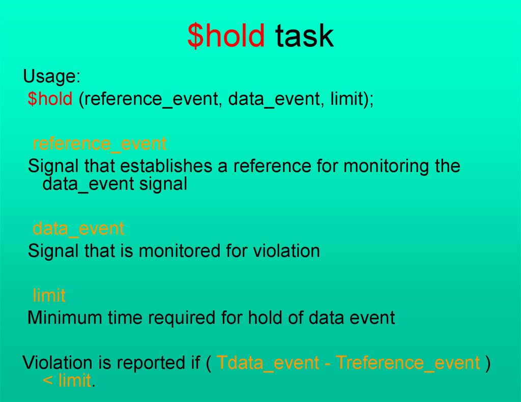
$hold taskUsage:
$hold (reference_event, data_event, limit);
reference_event
Signal that establishes a reference for monitoring the
data_event signal
data_event
Signal that is monitored for violation
limit
Minimum time required for hold of data event
Violation is reported if ( Tdata_event - Treference_event )
< limit.
192.
$hold taskexample
specify
$hold(posedge clear, data, 5);
$hold ( posedge CLK &&& CHKEN8A,
RSCIN, Trscx, notif_a_rscin )
endspecify
193.
$width CheckWidth of
the pulse
194.
$width CheckUsage:
$width(reference_event, limit);
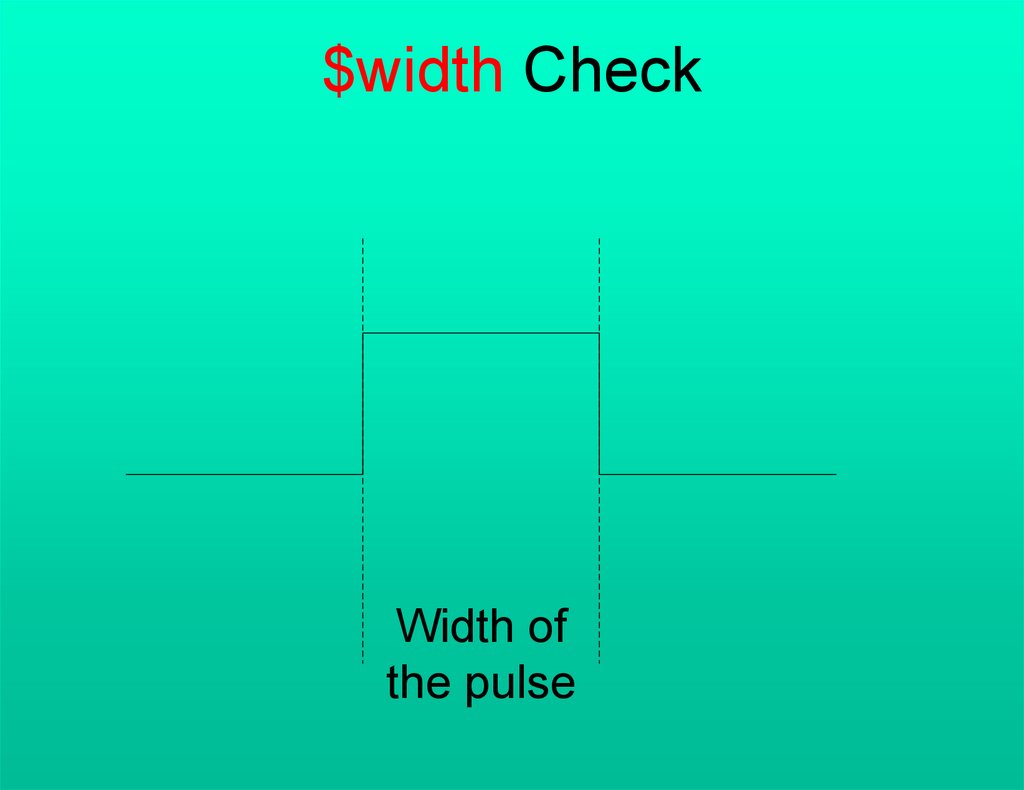
reference_event
Edge-triggered event (edge transition of a signal)
limit
Minimum width of the pulse
Violation is reported if ( Tdata_event –
Treference_event ) < limit.
195.
$width Checkexample
//width check is set.
//posedge of clear is the reference_event
//the next negedge of clear is the data_event
//Violation reported if Tdata - Tclk < 6
specify
$width (posedge clock, 6);
$width (negedge CLK, Tcl, notif_a_clk);
endspecify
196.
Delay Back-Annotation1. The designer writes the RTL description and
then performs functional simulation.
2. The RTL description is converted to a gatelevel netlist by a logic synthesis tool.
3. The designer obtains pre-layout estimates of
delays in the chip by using a delay calculator
and information about the IC fabrication
process. Then, the designer does timing
simulation or static timing verification of the
gate-level netlist, using these preliminary
values to check that the gate-level netlist
meets timing constraints.
197.
Delay Back-Annotation• The gate-level netlist is then converted to layout by
a place and route tool. The post-layout delay
values are computed from the resistance (R) and
capacitance (C) information in the layout. The R
and C information is extracted from factors such as
geometry and IC fabrication process.
• The post-layout delay values are back-annotated
to modify the delay estimates for the gate-level
netlist. Timing simulation or static timing
verification is run again on the gate-level netlist to
check if timing constraints are still satisfied.
• If design changes are required to meet the timing
constraints, the designer has to go back to the RTL
level, optimize the design for timing, and then
repeat Step 2 through Step 5.
198.
Delay Back-AnnotationRTL level description
Logic Synthesis
Delay
Calculator
Delay
Values
Gate-Level Netlist
Back
annotation
of post layout
delays
Place and Route
Delay
Calculator
Layout
Post Layout
Information
Implementation
199.
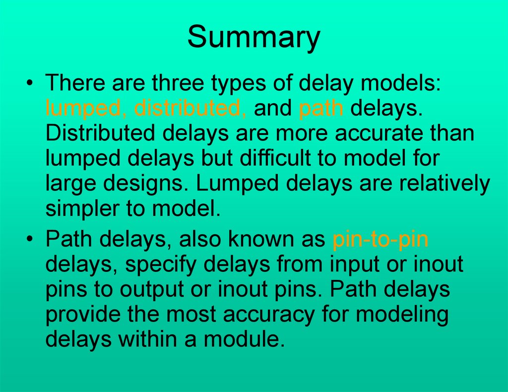
Summary• There are three types of delay models:
lumped, distributed, and path delays.
Distributed delays are more accurate than
lumped delays but difficult to model for
large designs. Lumped delays are relatively
simpler to model.
• Path delays, also known as pin-to-pin
delays, specify delays from input or inout
pins to output or inout pins. Path delays
provide the most accuracy for modeling
delays within a module.
200.
Summary• Specify blocks are the basic blocks for
expressing path delay information. In
modules, specify blocks appear separately
from initial or always blocks.
• Parallel connection and full connection are
two methods to describe path delays.
• Parameters can be defined inside the
specify blocks by specparam statements.
201.
Summary• Path delays can be conditional or
dependent on the values of signals in the
circuit. They are known as State
Dependent Path Delays (SDPD).
• Rise, fall, and turn-off delays can be
described in a path delay. Min, max, and
typical values can also be specified.
Transitions to x are handled by the
pessimistic method.
202.
Summary• Setup, hold, and width are timing checks
that check timing integrity of the digital
circuit. Other timing checks are also
available.
• Delay back-annotation is used to
resimulate the digital design with path
delays extracted from layout information.
This process is used repeatedly to obtain
a final circuit that meets all timing
requirements.
203.
Timing and Delays204.
Learning Objectives• Identify types of delay models, distributed,
lumped, and pin-to-pin (path) delays used in
Verilog simulation.
• Understand how to set path delays in a
simulation by using specify blocks.
• Explain parallel connection and full
connection between input and output pins.
• Understand how to define parameters inside
specify blocks by using specparam
statements.
205.
Learning Objectives• Describe state-dependent path delays.
• Explain rise, fall, and turn-off delays.
Understand how to set min, max, and typ
values.
• Define system tasks for timing checks
$setup, $hold, and $width.
• Understand delay back-annotation.
206.
Types of Delay ModelsThere are three types of delay models
used in Verilog:
Distributed
Lumped
Pin-to-pin (path)
delays.
207.
Distributed DelayM
a
b
#5
e
#4
c
d
f
#7
out
208.
ExampleDistributed Delays
//Distributed delays in gate-level modules
module M (out, a, b, c, d);
output out;
input a, b, c, d;
wire e, f;
//Delay is distributed to each gate.
and #5 a1(e, a, b);
and #7 a2(f, c, d);
and #4 a3(out, e, f);
endmodule
209.
ExampleDistributed Delays
//Distributed delays in data flow definition of a module
module M (out, a, b, c, d);
output out;
input a, b, c, d;
wire e, f;
//Distributed delay in each expression
assign #5 e = a & b;
assign #7 f = c & d;
assign #4 out = e & f;
endmodule
210.
Lumped DelayM
a
b
e
#11
c
d
f
out
211.
ExampleLumped Delay
//Lumped Delay Model
module M (out, a, b, c, d);
output out;
input a, b, c, d;
wire e, f;
and a1(e, a, b);
and a2(f, c, d);
and #11 a3(out, e, f);//delay only on the output gate
endmodule
212.
Pin-to-Pin DelaysM
a
b
e
out
c
f
d
Path a-e-out delay = 9 Path c-f-out delay = 11
Path b-e-out delay = 9 Path d-f-out delay = 11
213.
Path Delay Modelingpath delay - a delay between a source
(input or inout) pin and a destination
(output or inout) pin of a module.
The statements within specify and endspecify
keywords constitute a specify block.
214.
Specify Blocks• Assign pin-to-pin timing delays across
module paths
• Set up timing checks in the circuits
• Define specparam constants
215.
Specify Blocks//Pin-to-pin delays
module M (out, a, b, c, d);
output out;
input a, b, c, d;
wire e, f;
specify
(a => out) = 9;
(b => out) = 9;
(c => out) = 11;
(d => out) = 11;
endspecify
//gate instantiations
and a1(e, a, b);
and a2(f, c, d);
and a3(out, e, f);
endmodule
216.
Parallel connectionA parallel connection is specified by the
symbol =>
Usage:
( <source_field> => <destination_field>) =
<delay_value>;
217.
Parallel connectionSource
Field
0
0
1
1 Destination
Field
2
2
218.
Parallel connection//bit-to-bit connection. both a and out are single-bit
(a => out) = 9;
//vector connection. both a and out are 4-bit vectors
a[3:0], out[3:0]
//a is source field, out is destination field.
(a => out) = 9;
//the above statement is shorthand notation
//for four bit-to-bit connection statements
(a[0] => out[0]) = 9;
(a[1] => out[1]) = 9;
(a[2] => out[2]) = 9;
(a[3] => out[3]) = 9;
219.
Illegal parallel connection//illegal connection. a[4:0] is a 5-bit
//vector, out[3:0] is 4-bit.
//Mismatch between bit width of source
//and destination fields
(a => out) = 9; //bit width does not match.
220.
Full Conection• A full connection is specified by the
symbol *>.
• Usage:
( <source_field> *> <destination_field>)
= <delay_value>;
221.
Full connectionSource
Field
0
0
1
1 Destination
Field
2
2
222.
Full Connectionexample
//Full Connection
module M (out, a, b, c, d);
output out;
input a, b, c, d;
wire e, f;
//full connection
specify
(a,b *> out) = 9;
(c,d *> out) = 11;
endspecify
and a1(e, a, b);
and a2(f, c, d);
and a3(out, e, f);
endmodule
223.
Full Connection//a[31:0] is a 32-bit vector and out[15:0] is a 16// bit vector. Delay of 9 between each bit of a
//and every bit of out
specify
( a *> out) = 9; // you would need 32 X 16 = 352
// parallel connection
// statements to accomplish the
// same result! Why?
endspecify
224.
Edge-Sensitive Pathsif ( RSCEN )
( posedge CLK => ( RSCOUT : 1'bx )) = ( Tcrout,
Tcrout );
if ( ( !OEB & !BISTE & !AWT ) | ( !TOEB & BISTE &
!AWT ))
( posedge CLK => ( Q[0] : 1'bx )) = (Tcq, Tcq,Tcqx,
Tcq, Tcqx, Tcq);
(posedge clock => (out +: in)) = (10 , 8);
225.
specparam statements//Specify parameters using specparam statement
specify
//define parameters inside the specify block
specparam d_to_q = 9;
specparam clk_to_q = 11;
(d => q) = d_to_q;
(clk => q) = clk_to_q;
endspecify
226.
Conditional path delaysspecify
if (a) (a => out) = 9;
if (~a) (a => out) = 10;
if (b & c) (b => out) = 9;
if (~(b & c)) (b => out) = 13;
if ({c,d} == 2'b01)
(c,d *> out) = 11;
if ({c,d} != 2'b01)
(c,d *> out) = 13;
endspecify
227.
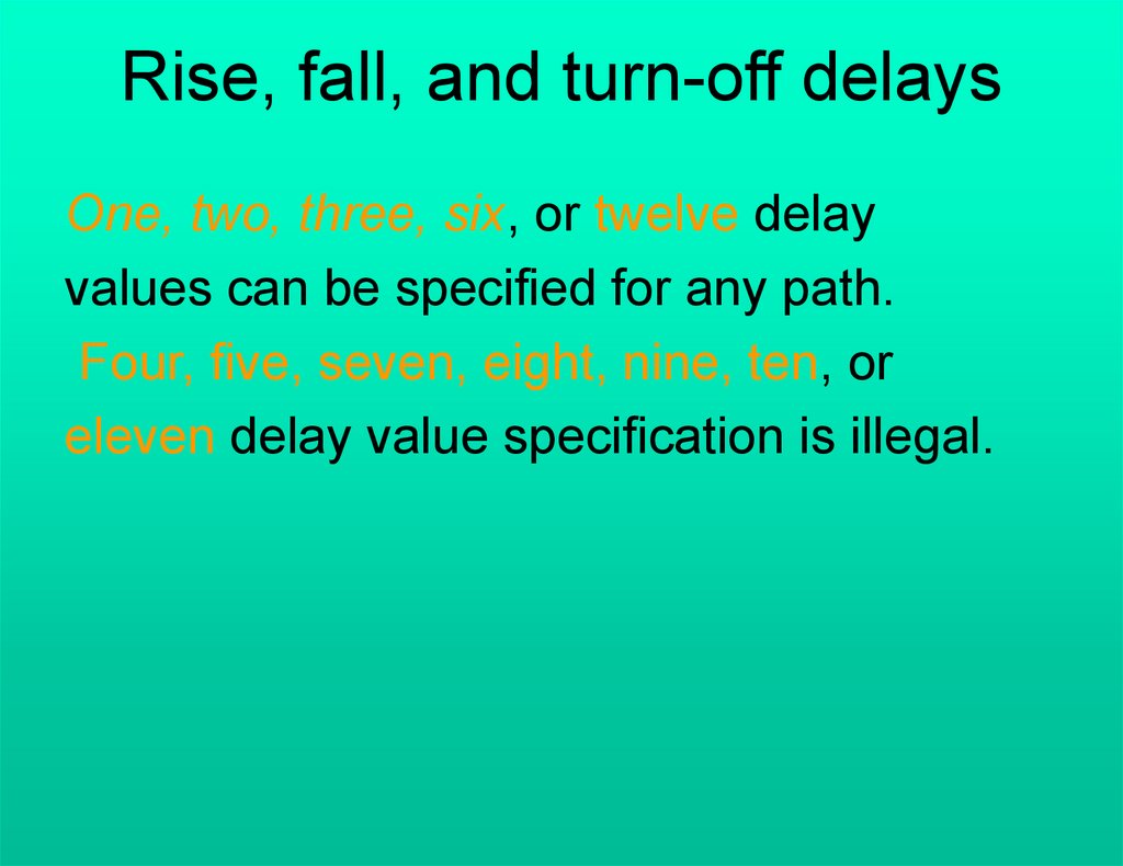
Rise, fall, and turn-off delaysOne, two, three, six, or twelve delay
values can be specified for any path.
Four, five, seven, eight, nine, ten, or
eleven delay value specification is illegal.
228.
Rise, fall, and turn-off delaysExample
//Specify one delay only. Used for all
//transitions.
specparam t_delay = 11;
(clk => q) = t_delay;
//Specify two delays, rise and fall
//Rise used for transitions 0->1, 0->z, z->1
//Fall used for transitions 1->0, 1->z, z->0
specparam t_rise = 9, t_fall = 13;
(clk => q) = (t_rise, t_fall);
229.
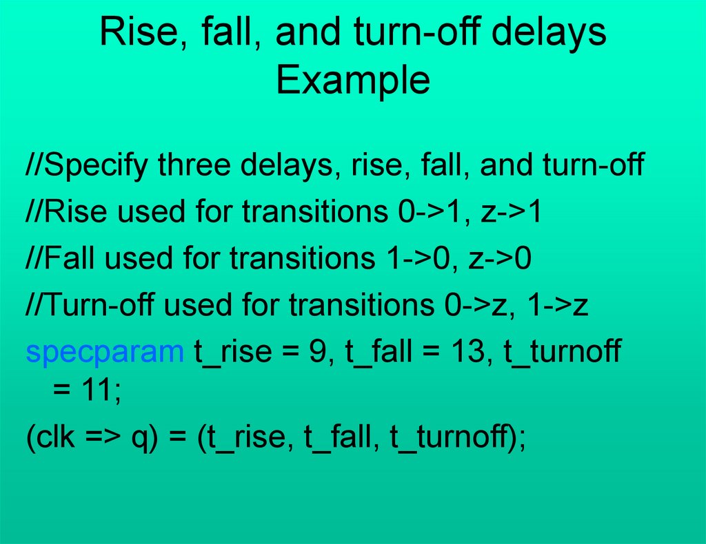
Rise, fall, and turn-off delaysExample
//Specify three delays, rise, fall, and turn-off
//Rise used for transitions 0->1, z->1
//Fall used for transitions 1->0, z->0
//Turn-off used for transitions 0->z, 1->z
specparam t_rise = 9, t_fall = 13, t_turnoff
= 11;
(clk => q) = (t_rise, t_fall, t_turnoff);
230.
Rise, fall, and turn-off delaysExample
//specify six delays.
//Delays are specified in order
//for transitions 0->1, 1->0, 0->z, z->1, 1->z,
//z->0. Order
//must be followed strictly.
specparam t_01 = 9, t_10 = 13, t_0z = 11;
specparam t_z1 = 9, t_1z = 11, t_z0 = 13;
(clk => q) = (t_01, t_10, t_0z, t_z1,
t_1z,t_z0);
231.
Rise, fall, and turn-off delaysExample
//specify twelve delays.
//Delays are specified in order
//for transitions 0->1, 1->0, 0->z, z->1, 1->z, z->0
//
0->x, x->1, 1->x, x->0, x->z, z->x.
//Order must be followed strictly.
specparam t_01 = 9, t_10 = 13, t_0z = 11;
specparam t_z1 = 9, t_1z = 11, t_z0 = 13;
specparam t_0x = 4, t_x1 = 13, t_1x = 5;
specparam t_x0 = 9, t_xz = 11, t_zx = 7;
(clk => q) = (t_01, t_10, t_0z, t_z1, t_1z, t_z0,
t_0x, t_x1, t_1x, t_x0, t_xz, t_zx );
232.
Min, max, and typicaldelays
//Specify three delays, rise, fall, and turn-off
//Each delay has a min:typ:max value
specparam t_rise = 8:9:10, t_fall = 12:13:14,
t_turnoff = 10:11:12;
(clk => q) = (t_rise, t_fall, t_turnoff);
+mindelays, +typdelays, +maxdelays
233.
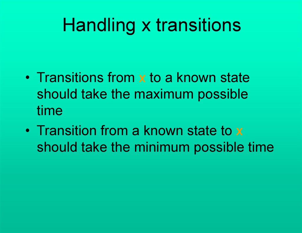
Handling x transitions• Transitions from x to a known state
should take the maximum possible
time
• Transition from a known state to x
should take the minimum possible time
234.
Handling x transitions//Six delays specified .
//for transitions 0->1, 1->0, 0->z, z->1, 1->z, z>0
specparam t_01 = 9, t_10 = 13, t_0z = 11;
specparam t_z1 = 9, t_1z = 11, t_z0 = 13;
(clk => q) = (t_01, t_10, t_0z, t_z1, t_1z, t_z0);
235.
Handling x transitions0->x min(t_01, t_0z) = 9
x->0 max(t_10, t_z0) = 13
1->x min(t_10, t_1z) = 11
x->1 max(t_01, t_z1) = 9
z->x min(t_z0, t_z1) = 9
x->z max(t_1z, t_0z) = 11
236.
Timing Checks$setup and $hold checks
• the setup time is the minimum time the
data must arrive before the active clock
edge.
• The hold time is the minimum time the
data cannot change after the active
clock edge.
237.
$setup and $hold checksclock
data
setup
data
hold
data
238.
$setup taskUsage:
$setup(data_event, reference_event, limit);
data_event : Signal that is monitored for violations
reference_event : Signal that establishes a
reference for monitoring the data_event signal
Limit : Minimum time required for setup of data
event
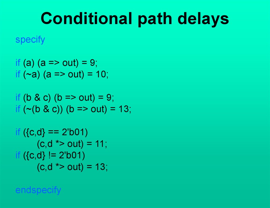
239.
$setup taskexample
specify
$setup(data, posedge clock, 3);
$setup ( RSCEN, posedge CLK, Tsc);
endspecify
240.
$hold taskUsage:
$hold (reference_event, data_event, limit);
reference_event
Signal that establishes a reference for monitoring the
data_event signal
data_event
Signal that is monitored for violation
limit
Minimum time required for hold of data event
Violation is reported if ( Tdata_event - Treference_event )
< limit.
241.
$hold taskexample
specify
$hold(posedge clear, data, 5);
$hold ( posedge CLK &&& CHKEN8A,
RSCIN, Trscx, notif_a_rscin )
endspecify
242.
$width CheckWidth of
the pulse
243.
$width CheckUsage:
$width(reference_event, limit);
reference_event
Edge-triggered event (edge transition of a signal)
limit
Minimum width of the pulse
Violation is reported if ( Tdata_event –
Treference_event ) < limit.
244.
$width Checkexample
//width check is set.
//posedge of clear is the reference_event
//the next negedge of clear is the data_event
//Violation reported if Tdata - Tclk < 6
specify
$width (posedge clock, 6);
$width (negedge CLK, Tcl, notif_a_clk);
endspecify
245.
Delay Back-Annotation1. The designer writes the RTL description and
then performs functional simulation.
2. The RTL description is converted to a gatelevel netlist by a logic synthesis tool.
3. The designer obtains pre-layout estimates of
delays in the chip by using a delay calculator
and information about the IC fabrication
process. Then, the designer does timing
simulation or static timing verification of the
gate-level netlist, using these preliminary
values to check that the gate-level netlist
meets timing constraints.
246.
Delay Back-Annotation• The gate-level netlist is then converted to layout by
a place and route tool. The post-layout delay
values are computed from the resistance (R) and
capacitance (C) information in the layout. The R
and C information is extracted from factors such as
geometry and IC fabrication process.
• The post-layout delay values are back-annotated
to modify the delay estimates for the gate-level
netlist. Timing simulation or static timing
verification is run again on the gate-level netlist to
check if timing constraints are still satisfied.
• If design changes are required to meet the timing
constraints, the designer has to go back to the RTL
level, optimize the design for timing, and then
repeat Step 2 through Step 5.
247.
Delay Back-AnnotationRTL level description
Logic Synthesis
Delay
Calculator
Delay
Values
Gate-Level Netlist
Back
annotation
of post layout
delays
Place and Route
Delay
Calculator
Layout
Post Layout
Information
Implementation
248.
Summary• There are three types of delay models:
lumped, distributed, and path delays.
Distributed delays are more accurate than
lumped delays but difficult to model for
large designs. Lumped delays are relatively
simpler to model.
• Path delays, also known as pin-to-pin
delays, specify delays from input or inout
pins to output or inout pins. Path delays
provide the most accuracy for modeling
delays within a module.
249.
Summary• Specify blocks are the basic blocks for
expressing path delay information. In
modules, specify blocks appear separately
from initial or always blocks.
• Parallel connection and full connection are
two methods to describe path delays.
• Parameters can be defined inside the
specify blocks by specparam statements.
250.
Summary• Path delays can be conditional or
dependent on the values of signals in the
circuit. They are known as State
Dependent Path Delays (SDPD).
• Rise, fall, and turn-off delays can be
described in a path delay. Min, max, and
typical values can also be specified.
Transitions to x are handled by the
pessimistic method.
251.
Summary• Setup, hold, and width are timing checks
that check timing integrity of the digital
circuit. Other timing checks are also
available.
• Delay back-annotation is used to
resimulate the digital design with path
delays extracted from layout information.
This process is used repeatedly to obtain
a final circuit that meets all timing
requirements.