


 Информатика
Похожие презентации:


")

Introduction to the computing device design using the FPGA technology
1.
SSD ICM&MG SB RAS Summer SchoolIntroduction to
the computing device design
using the FPGA technology
2015
2.
Outline1.Introduction
2.FPGA architecture
3.Developer’s tools
4.Examples of small projects
5.Existing libraries and
components
6.Efficiency of FPGA-based
projects
7.Miscellaneous and conclusion
3.
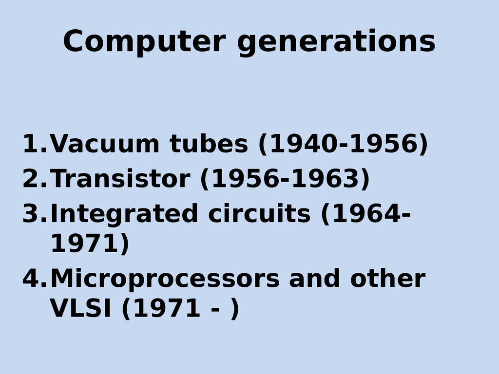
Part 1. Introduction1.1. Computer generations
1.2. Problem: The tyranny of numbers
1.3. Solution: Integrated Circuits
4.
Computer generations1.Vacuum tubes (1940-1956)
2.Transistor (1956-1963)
3.Integrated circuits (19641971)
4.Microprocessors and other
VLSI (1971 - )
5.
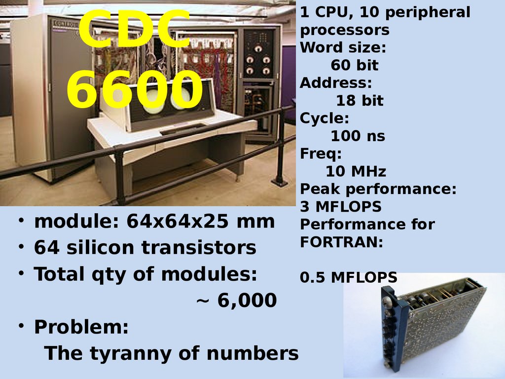
CDC6600
1 CPU, 10 peripheral
processors
Word size:
60 bit
Address:
18 bit
Cycle:
100 ns
Freq:
10 MHz
Peak performance:
3 MFLOPS
Performance for
FORTRAN:
• module: 64x64x25 mm
• 64 silicon transistors
• Total qty of modules:
0.5 MFLOPS
~ 6,000
• Problem:
The tyranny of numbers
6.
Timeline of IC evolution• 1947 – Bell Labs - the invention of the
transistor
• 1952 – Geoffrey Dummer - the idea of IC
• 1953 – Harwick Johnson – patent for a
method of forming transistors, resistors
and capacitance on a single chip
• 1958 – Jack Kilby, Texas Instruments – the
first IC built
• 1961-1962 – the first applications (AF,
ICBM, calculator)
7.
Apollo Guidance ComputerFreq: 2 МГц
Word size: 16 bits
RAM: 2K words
ROM: 36K words
Weight:
32 kg
Power
consumption: 55
W
8.
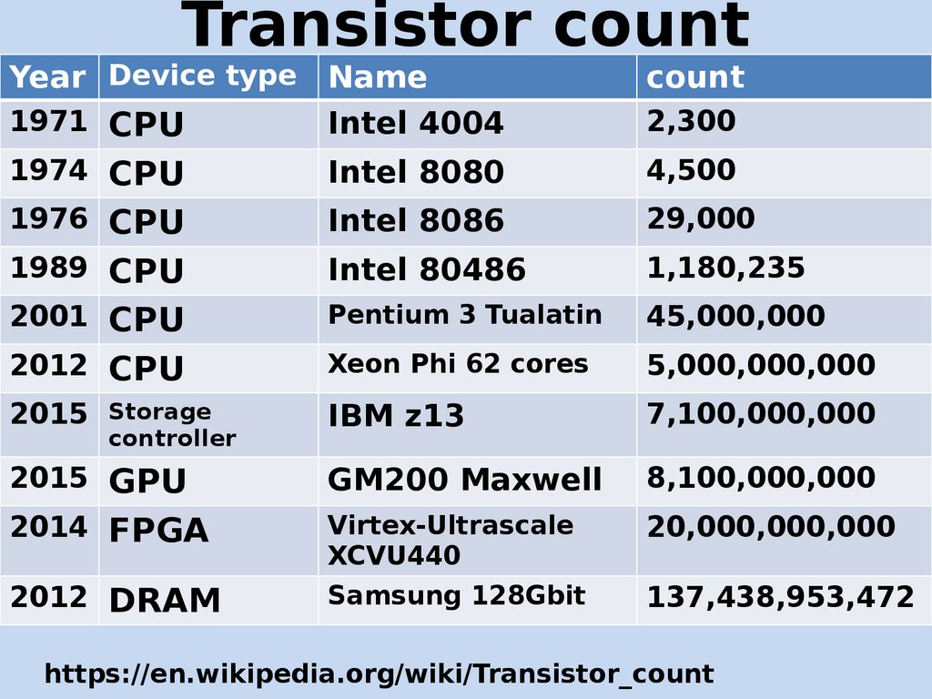
Transistor countYear Device type Name
1971 CPU
Intel 4004
count
1974 CPU
Intel 8080
4,500
1976 CPU
Intel 8086
29,000
1989 CPU
Intel 80486
1,180,235
2001 CPU
Pentium 3 Tualatin
45,000,000
2012 CPU
Xeon Phi 62 cores
5,000,000,000
2015 Storage
IBM z13
7,100,000,000
2015 GPU
GM200 Maxwell
8,100,000,000
2014 FPGA
Virtex-Ultrascale
XCVU440
20,000,000,000
2012 DRAM
Samsung 128Gbit
137,438,953,472
controller
2,300
https://en.wikipedia.org/wiki/Transistor_count
9.
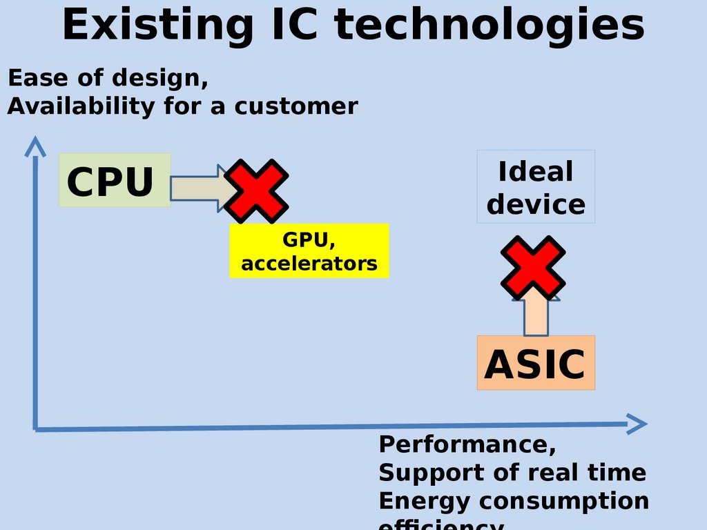
Existing IC technologiesEase of design,
Availability for a customer
Ideal
device
CPU
GPU,
accelerators
ASIC
Performance,
Support of real time
Energy consumption
10.
Problems of existing IC technologiesCPU – the easy way
(easy to develop, cheap hardware, slow performance)
• Performance growth limits
• Power wall; technological limits
• Problem of connections; architectural limits
• Energy consumption – inefficient ratio
performance/energy
• Architecture is a Barely satisfactory compromise for a
wide specter of applications – no way to fine tune
structure for an app or to exploit the full inner
parallelism of an application
ASIC – the hard way
(hard to develop, expensive hardware, high performance)
• Expensive to design and produce
• Once produced, no way to modify functionality
11.
Part 2. FPLD, FPGA architecture2.1. Purpose, main advantages
2.2. Classification of field programmable logic
devices
2.3. Structure of FPGA
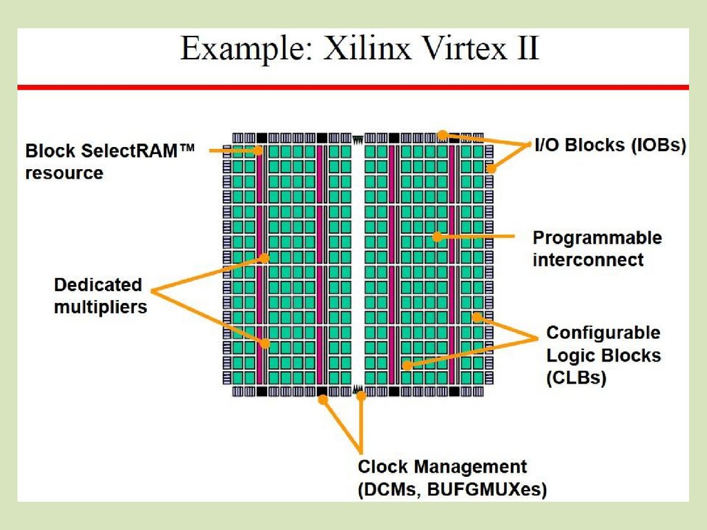
2.4. Examples of real world FPGA chips
12.
FPLD main features• An implemented function can be
reprogrammed by a user multiple times
• The availability of several types of
functional blocks (for processing,
communication and storage).
• The blocks can work simultaneously.
• The configuration of each block is
reprogrammable
• The connections between blocks are
reprogrammable
13.
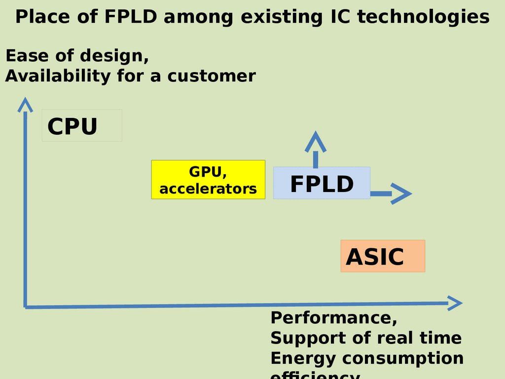
Place of FPLD among existing IC technologiesEase of design,
Availability for a customer
CPU
GPU,
accelerators
FPLD
ASIC
Performance,
Support of real time
Energy consumption
14.
Advantages of FPLD (vs. CPU)• Possibility to reach the maximum possible
(for an application) degree of parallelism.
• Ability to synthesize a structure suitable
for a particular task with fine tuning of
various parameters (arbitrary bus width,
register size, word size, …).
• No bottlenecks, as unlike von Neumann
there are no unique centralized functional
blocks. Logic, communication and storage
are all decentralized/distributed.
15.
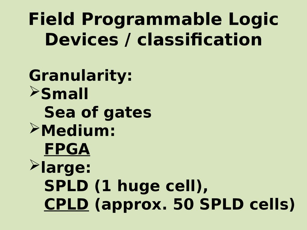
Field Programmable LogicDevices / classification
Granularity:
Small
Sea of gates
Medium:
FPGA
large:
SPLD (1 huge cell),
CPLD (approx. 50 SPLD cells)
16.
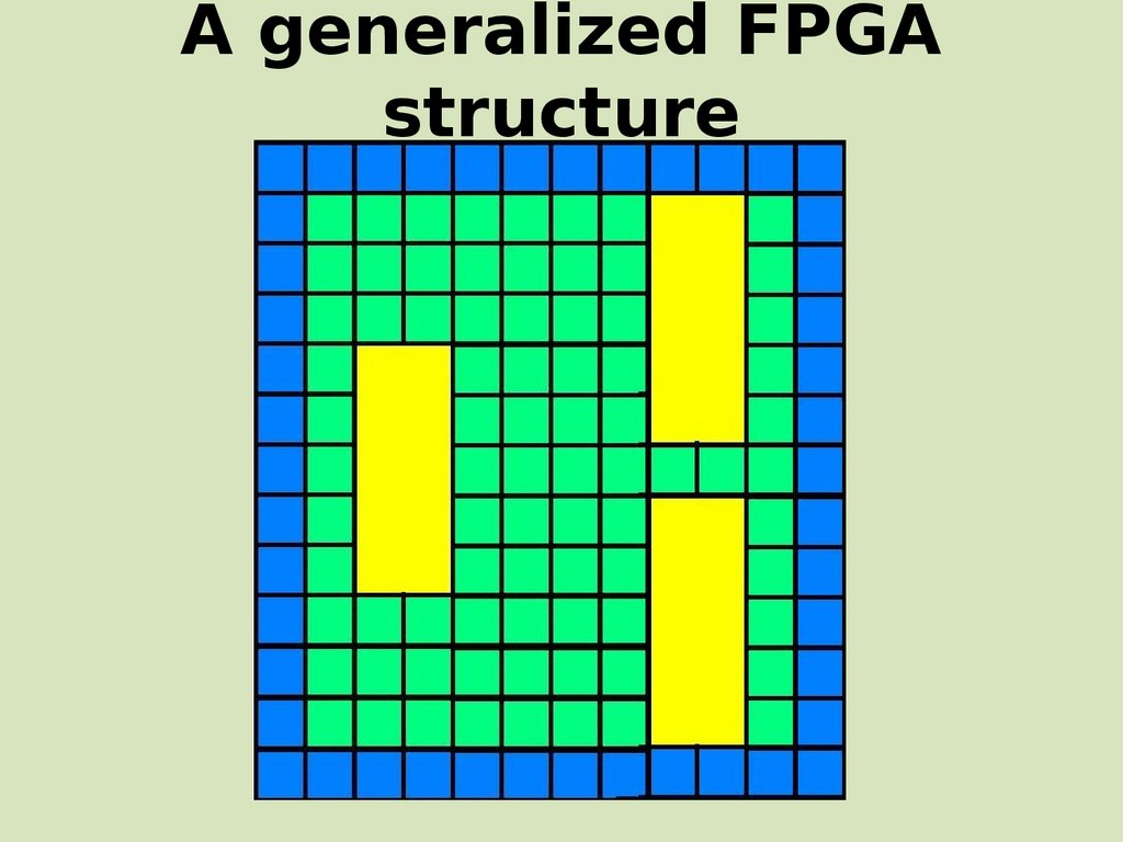
A generalized FPGAstructure
17.
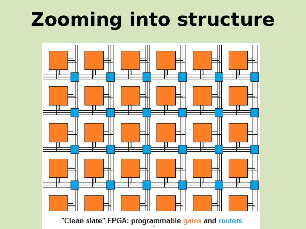
Types of functional cells• Logic cells - processing
• Commutators – communications in
chip
• I/O macro cells – communication
with the world
• Block memory - storage
• Arithmetic devices
• Clock signal management - control
18.
Zooming into structure19.
Logic cell interface partReprogrammable
truth table
Input
wires
Output
wires
20.
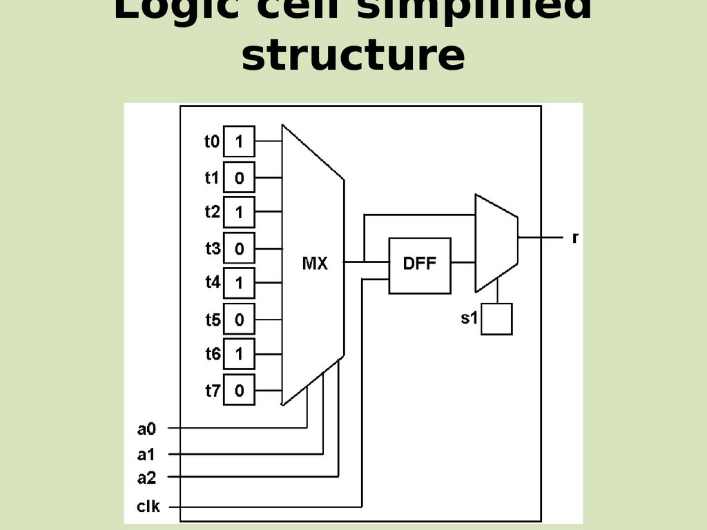
Logic cell simplifiedstructure
21.
Composition of logiccells
22.
Comutator cell23.
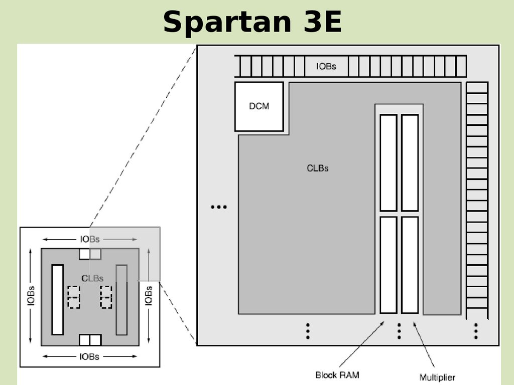
Spartan 3EGates: 100K – 1.6M
Logic cells: до 33,192.
I/O channel transfer rate: 622Mb/s
DDR SRAM transfer rate: 333 Mb/s
Total size of RAM blocks: up to 648 Kb
Other macro cells: 18-bit multipliers, shift
registers, multiplexers
• Clock signal frequency: 5-300MHz
24.
Spartan 3E25.
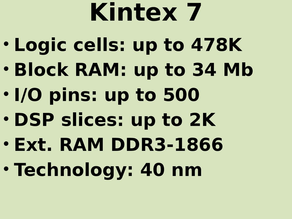
Kintex 7• Logic cells: up to 478K
• Block RAM: up to 34 Mb
• I/O pins: up to 500
• DSP slices: up to 2K
• Ext. RAM DDR3-1866
• Technology: 40 nm
26.
27.
Part 3. Developer tools3.1. Hardware tools
3.2. Hardware description languages
3.3. Software tools
28.
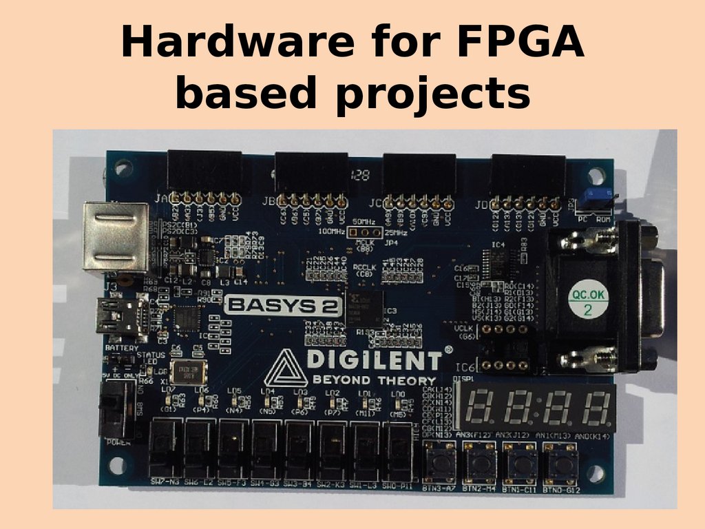
Hardware for FPGAbased projects
29.
Developer board / Papilio ProUSB:
I/O pins:
SDRAM:
Flash:
2 channels
48
64 Mb
64Mb
30.
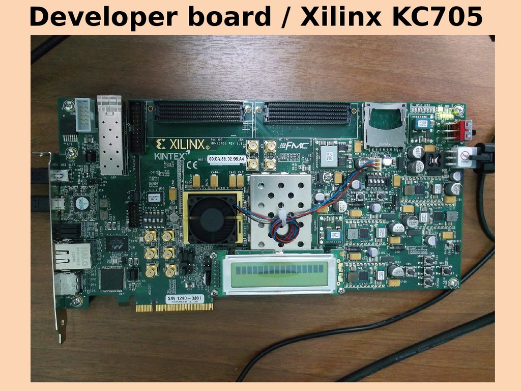
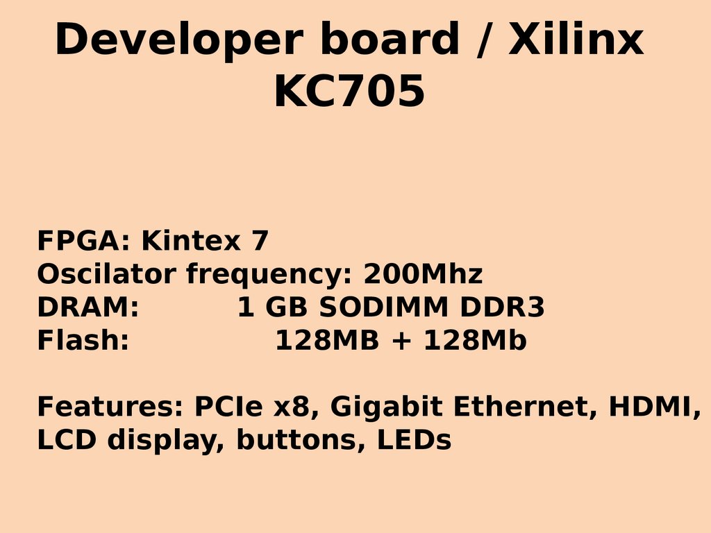
Developer board / Xilinx KC70531.
Developer board / XilinxKC705
FPGA: Kintex 7
Oscilator frequency: 200Mhz
DRAM:
1 GB SODIMM DDR3
Flash:
128MB + 128Mb
Features: PCIe x8, Gigabit Ethernet, HDMI,
LCD display, buttons, LEDs
32.
VHDLSyntax:
derived from Ada (derivative of Algol
languages)
Used for:
1)simulation of digital electronic schemes;
2)synthesis of schemes for ASIC and FPGA.
(supported by all main FPGA vendors)
Basic methods for scheme description:
3) behavior-oriented;
4) structural;
5) import of external components (e.g. IP-s)
33.
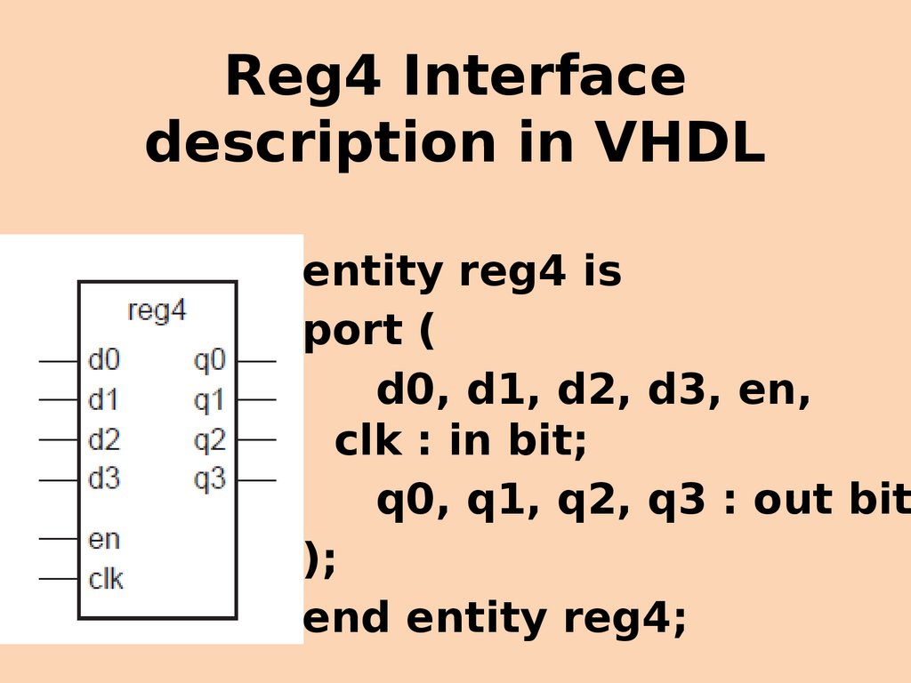
Reg4 Interfacedescription in VHDL
entity reg4 is
port (
d0, d1, d2, d3, en,
clk : in bit;
q0, q1, q2, q3 : out bit
);
end entity reg4;
34.
Behavior-oriented implementationof Reg4
architecture behav of reg4 is
begin
storage : process is
variable stored_d0, stored_d1,
stored_d2, stored_d3 : bit;
begin
wait until clk = '1';
if en = '1' then
stored_d0 := d0;
stored_d1 := d1;
stored_d2 := d2;
stored_d3 := d3;
end if;
q0 <= stored_d0 after 5
q1 <= stored_d1 after 5
q2 <= stored_d2 after 5
q3 <= stored_d3 after 5
end process storage;
end architecture behav;
ns;
ns;
ns;
ns;
35.
Structural implementation of Reg4interface (1/3)
36.
Structural implementation of Reg4interface (3/3)
architecture struct of reg4 is
signal int_clk : bit;
begin
bit0 : entity work.d_ff(basic)
port map (d0, int_clk, q0);
bit1 : entity work.d_ff(basic)
port map (d1, int_clk, q1);
bit2 : entity work.d_ff(basic)
port map (d2, int_clk, q2);
bit3 : entity work.d_ff(basic)
port map (d3, int_clk, q3);
gate : entity work.and2(basic)
port map (en, clk, int_clk);
end architecture struct;
37.
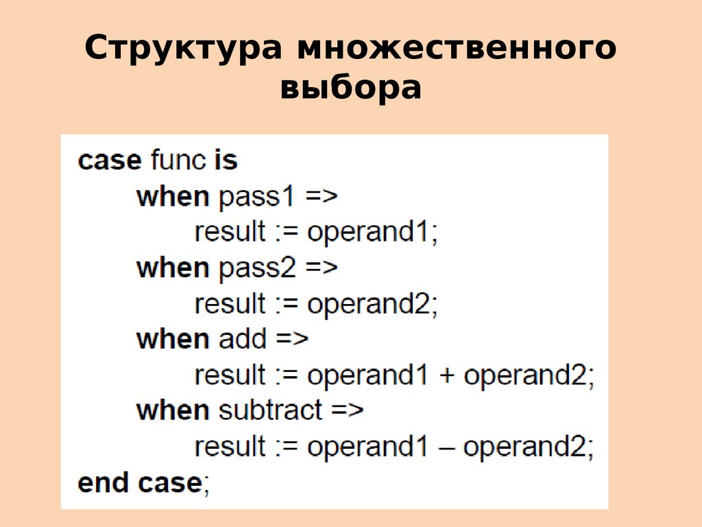
Структура множественноговыбора
38.
Структура множественноговыбора
39.
Part 5. Existing libraries andcomponents
5.1. A few examples of software CPUs
5.2. Overview of available free projects
40.
Existing software CPUsGNU, open source:
• Angelus Research Forth
Processor
• ZPU
• OpenRISC
Proprietary:
• picoBlaze
• microBlaze
41.
Angelus Research ForthProcessor
• Stack architecture with machine
code oriented to Forth program
execution
• Word size:
• Address size:
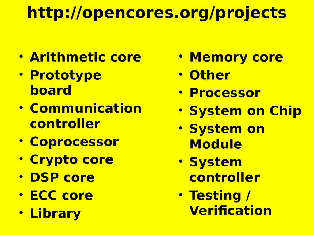
42.
http://opencores.org/projects• Arithmetic core
• Prototype
board
• Communication
controller
• Coprocessor
• Crypto core
• DSP core
• ECC core
• Library
Memory core
Other
Processor
System on Chip
System on
Module
• System
controller
• Testing /
Verification
43.
Part 6. Efficiency of FPGAbased projects
6.1. Generalized Memory hierarchy
6.2. FPGA friendly architectures
44.
Generalized memory hierarchy• Distributed registers – many, small
size, very fast, on chip
• Block RAM – rather limited number
of blocks (~12-80), medium size
(typically 2-9 KB), fast, on chip
• External RAM – can be huge (size
depends on a particular board
used, can be several GB, VERY
SLOW!)
45.
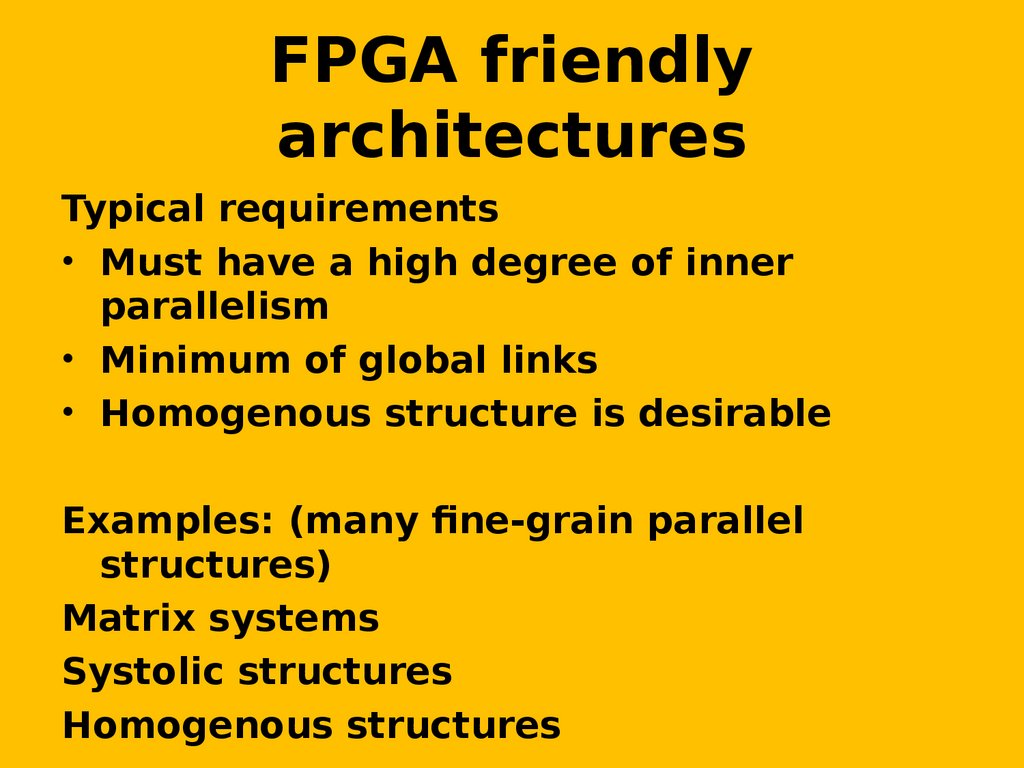
FPGA friendlyarchitectures
Typical requirements
• Must have a high degree of inner
parallelism
• Minimum of global links
• Homogenous structure is desirable
Examples: (many fine-grain parallel
structures)
Matrix systems
Systolic structures
Homogenous structures
46.
Part 7. Miscellaneous7.1.
7.2.
7.3.
7.4.
Examples of out-of-box developments on FPGA
Overview of alternative FPGA dev technologies
Perspectives
Conclusions
47.
PerspectivesTechnological advances:
• Adapting 8 nm in 2016-2017
(Altera+TSMC)
• Switching to 3D IC with optical inter-layer
connections (more distant future)
Architectural advances
• Fusion with CPUs, SoCs – hybrid devices
(evolving even as I speak)
• Evolution of architectures other than
classical FPLD (Reconfigurable computing
devices) – a bit more distant future