


 Электроника
Похожие презентации:


")


Gowin Semiconductor Corporation
1.
GOWIN Semiconductor CorporationCorporate Presentation
www.gowinsemi.com
Dec 2020
2.
Agenda1)
2)
3)
4)
5)
6)
7)
8)
9)
10)
11)
12)
Dec 01, 2020
Introduction
GOWIN FPGA Product Families
Embedded Processors
On-Chip Memory Options
Pin Compatible Devices
Automotive Parts
LittleBee GW1N & GW1NR
LittleBee GW1NS & GW1NSE µSoC
LittleBee GW1NZ Ultra-Low Power
LittleBee GW1NRF Bluetooth Low Energy
Arora GW2A, GW2AR, GW2ANR & GW2AN
Arora Next Generation GW5AT
13)
14)
15)
16)
17)
18)
19)
20)
21)
22)
©GOWIN Semiconductor
GOWIN Product Roadmap
Website Registration
GOWIN Development Tools
IP Core Examples
GoAI 2.0 Machine Learning
GoAI 2.0 Eval Boards
GW1NRF Bluetooth Development Kit
GW1N Development Boards
GW1NS µSoC Development Boards
Arora GW2A Development Boards
2
3.
GOWIN European Contacts & SupportMajor R&D Centers
Guangzhou
Shanghai
Hong Kong
Jinan
GMT (UTC) Nov to March
BST (UTC + 1) April to Oct
United Kingdom
GOWIN Semiconductor Europe
3rd Floor, The Senate,
Southernhay Gardens,
Exeter EX1 1UG
www.gowinsemi.com
Dec 01, 2020
International Sales
Mike Furnival
Director of Sales
GOWIN
Semiconductor
Europe
Danny Fisher
Senior FAE EMEA
GOWIN
Semiconductor
Europe
[email protected]
[email protected]
Mobile +44 7836 591426
Skype: Mike.Furnival
Mobile: +44 7779 306 569
Skype: danny_13344
©GOWIN Semiconductor
Guangzhou China (HQ)
United Kingdom
Hong Kong
San Jose USA
Korea
Shandong China
Shenzhen (South China)
Shanghai (East China)
Beijing (North China)
Wuhan (Central & SW China)
3
4.
GOWIN Company OverviewProviding easy to use, high performance, low-cost FPGA solutions for
consumer, industrial, automotive, and communications applications.
Locations:
Manufacturing:
Guangdong, China (Corp HQ)
San Jose, California (US HQ)
Hong Kong (Asia HQ)
Shandong, Shanghai, Shenzhen
Founded: 2014
Silicon: 2016
First revenues: 2017
World’s fastest growing FPGA Company
FPGA Devices: Flash and SRAM Based
Low-Density / Low Power (LUTs < 10K): GW1N, GW1NR, GW1NS, GW1NRF
Scalable manufacturing capabilities
with world-class partners.
Mid-Density (10K < LUTs < 100K): GW2A, GW2AR, GW2ANR
High-Density (LUTs > 100K): GW5AT, GW4ST
Key Partners
Awards and Recognition
China Annual Creativity in
Electronics
2018
Dec 01, 2020
©GOWIN Semiconductor
2015 & 2016
Most
Remarkable
Global
Technology
Startup
4
5.
GOWIN FPGA FamiliesFlash Based FPGAs
SRAM Based FPGAs
1-10K Logic Element Density
20-55K Logic Element Density
Consumer, Mobile and IoT
Communications, Industrial and Automotive
As small as 1.8 x 1.8mm
As small as 8x8mm
Interface Bridging and Multiplexing
Up to 607 user interface pins
1.2 Gbps LVDS, DDR3, MIPI D-PHY, PCI
High Speed Interfacing and IO Expansion
Industrial, Commercial and Server
TQFP, QFN and BGA (0.8mm) Packaging
CPLD Replacement, Power/Platform Management
Differentiating FPGA Features
Hardened MCUs
On-Chip Memory
More Interfaces
Ultra-Low Power
Security
Arm Cortex-M3
Up to 16MB
ADC, USB, SPMI, I3C
10µW Sleep
PUF Based RoT
Dec 01, 2020
©GOWIN Semiconductor
5
6.
GOWIN FPGA Product FamiliesGOWIN FPGA Family Devices
Product Features
*S
Extended Memory
On-Chip SRAM
*R
Arora plus SRAM & Flash
Dec 01, 2020
1K
Ultra-Low Power
GW1NS
2K, 4K
GW1NR
1K, 4K, 9K
GW1NSR
2K, 4K
MCU + Memory
GW1NSE
2K, 4K
MCU + Security
GW1NSER
2K. 4K
MCU + Security +
Memory
GW1NRF
4K
MCU + Security +
RF Transceiver
GW2A
20K, 55K
GW2AR
20K
*N
GW2AN
20K
On-Chip NOR Flash
*NR
GW2ANR
20K
On-Chip Memory
Plus, NOR Flash
GW2A* 20-55K
Logic Element Density
*SR
*R
*SE
*SER
Security
SRAM PUF Root-of-Trust
Arora plus Flash
GW1NZ
SRAM-Based FPGA
Hard MCU
ARM Cortex-M3
ARC EM4
Bluetooth Low Energy
RF Transceiver
Flash-Based FPGA
Flash-Based FPGA
*Z
Arora
1K, 2K, 4K, 9K
Arora
Ultra-Low Power
SPMI Power Management
LittleBee
GW1N
LittleBee
GW1N* 1-10K
Logic Element Density
Product Series Density (LUTs)
*RF
©GOWIN Semiconductor
Embedded
Hardcore MCU
Extended Memory
N/A
RAM-Based FPGA
N/A
On-Chip Memory
6
7.
GOWIN FPGA Embedded ProcessorsGOWIN FPGA Embedded Processor Options
Dec 01, 2020
Device Family /
CLK Freq (MHz)
Core
Instruction Set
IP Resources (LUTs)
DMIPS/MHz
CoreMark®/MHz
PicoRV32
RISC-V
Softcore 2K
0.516
-
GW2A*: 50
GW1N* : 50
Andes N25
RISC-V AndeStar™ V5
Softcore 10K
GW2A18: 1.94
GW2A55: 2.29
-
GW2A*: 50
Cortex M1
ARM Thumb, Thumb-2
Softcore
(5K to 21K)
0.8
1.85
GW2A*: 75
GW1N9: 40
Cortex M3
ARM Thumb, Thumb-2
Softcore
(18K to 37K)
1.25 to 1.89
3.34
GW2A55: 25
Cortex M3
ARM Thumb, Thumb-2
Hardcore N/A
1.25 to 1.89
3.34
GW1NS*-2C: 30
GW1NS*-4C: 100
ARC EM4
Synopsys ARCv2
Hardcore N/A
1.77
3.41
GW1NRF: 24
©GOWIN Semiconductor
7
8.
GOWIN FPGA On-Chip Memory Options128Mbits DDR
pSRAM
Data Width: 16-bits
Clock Freq: 166MHz
128Mbits DDR
DDR
Data Width: 16-bits
Clock Freq: 200MHz
Hyper
RAM
Data Width: 8-bits
Clock Freq: 200MHz
32Mbits SDR
64Mbits SDR
64Mbits DDR
SDRAM
Data Width: 32-bits
Clock Freq: 166MHz
FLASH
Data Width: 1-bit
Clock Freq: 120MHz
GOWIN FPGA Embedded Memory Options
Device
GW1NR
GW1NSR-4C
GW1NSR–2/2C
GW1NSR–4/4C
GW2AR
GW2ANR
Dec 01, 2020
Memory Technology
Capacity
(MBytes)
Data Width
(Bits)
Clock (MHz)
Comments
NOR Flash (FN32G)
4
100
1
Additional on-chip FLASH Memory
SDR SDRAM
8
Up to 200
16
Max Clock Speed depends on package.
DDR pSRAM
Up to 16
166 (equivalent DDR332)
16
32 (MG100)
Memory Capacity depends on package.
NOR Flash (QN48G)
4
120
1
Flash Memory supports additional ARM instruction code.
8
Hardcore ARM Cortex M3
Memory Capacity depends upon memory technology & package.
DDR HyperRAM (QN48P) Up to 8
200 (equivalent DDR400)
DDR pSRAM
Up to 4
166 (equivalent DDR332)
8
Max Capacity depends upon memory technology & package.
DDR pSRAM
Up to 8
166 (equivalent DDR332)
16
Max Capacity depends upon memory technology & package.
SDR SDRAM
8
166
32
DDR SDRAM
16
200/250
16
DDR pSRAM
8
166 (equivalent DDR332)
16
SDR SDRAM
8
166
32
NOR Flash
4
120
1
©GOWIN Semiconductor
Max Clock Speed depends on package.
Flash Memory
8
9.
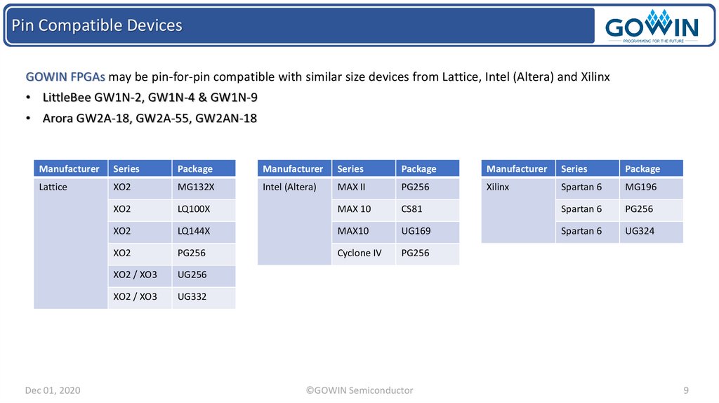
Pin Compatible DevicesGOWIN FPGAs may be pin-for-pin compatible with similar size devices from Lattice, Intel (Altera) and Xilinx
• LittleBee GW1N-2, GW1N-4 & GW1N-9
• Arora GW2A-18, GW2A-55, GW2AN-18
Manufacturer
Series
Package
Manufacturer
Series
Package
Manufacturer
Series
Package
Lattice
XO2
MG132X
Intel (Altera)
MAX II
PG256
Xilinx
Spartan 6
MG196
XO2
LQ100X
MAX 10
CS81
Spartan 6
PG256
XO2
LQ144X
MAX10
UG169
Spartan 6
UG324
XO2
PG256
Cyclone IV
PG256
XO2 / XO3
UG256
XO2 / XO3
UG332
Dec 01, 2020
©GOWIN Semiconductor
9
10.
Automotive Parts – Available Q1/Q2 2021CAN 2.0 Controller IP
AEC-Q100 Level-2 Certification
• -40oC to +105oC
Sensor Interfaces
LittleBee GW1N-4 QN88
• Qualification Completes Q1 2021
Arora GW2A18 QN88
• Qualification Completes Q2 2021
LittleBee GW1NZ QN48
• Qualification Started
Dec 01, 2020
Display Interfaces & Bridging
• MIPI IP & Ref Designs
• LVDS
©GOWIN Semiconductor
10
11.
LittleBee GW1N (Base Family)Flash-Based, Non-Volatile, Instant On, Low Power, Low Cost, Small Package Options
Resource
GW1N-1
GW1N-2
GW1N-4
GW1N-9
.
Available Q1-2021
LUT4
1152
2304
4608
8640
Flip-Flop
864
2304
3456
6480
Shadow S-SRAM (Bits)
-
-
-
17280
Block B-SRAM (bits)
72K
72K
180K
468K
B-SRAM Blocks
4
4
10
26
User Flash (Bits)
96K
256K
256K
608K
Mult 18x18
-
-
16
20
PLLs
1
1
2
2
I/O Banks
4
6
4
4
Max I/O
120
126
218
276
Core Voltage ZV
-
0.9V
-
-
Core Voltage LV
1.2V
1.2V
1.2V
1.2V
Core Voltage UV
1.8V/2.5V/3.3V
1.8V/2.5V/3.3V
2.5V/3.3V
2.5V/3.3V
Only LQ100X
Dec 01, 2020
©GOWIN Semiconductor
11
12.
LittleBee GW1NR with On-Chip MemoryOn-Chip Memory up to 128Mbits* (16KBytes) *package dependent
Resource
GW1NR-1
GW1NR-4/4B GW1NR-9
LUT4
1152
4608
8640
Flip-Flop
864
3456
6480
Shadow S-SRAM (Bits)
-
-
17280
Block B-SRAM (Bits)
72K
180K
468K
B-SRAM Blocks
4
10
26
User Flash (Bits)
96K
256K
608K
Memory SDR SDRAM (Bits)
-
64M (QN88)
64M (QN88)
Memory DDR pSRAM (Bits)
-
32M (QN88P)
64M
(QN88P/LQ144P/MG100PT/MG100PS)
.
On-Chip Memory
System-in-Package
(SiP) Technology
64M (MG81P)
128M
(MG100P/MG100PF/MG100PA)
Memory NOR Flash (Bits)
4M (FN32G)
-
-
Mult 18x18
-
16
20
PLLs
1
2
2
Max I/O
120
218
276
Core Voltage LV
1.2V
1.2V
1.2V
Core Voltage UV
-
2.5V/3.3V
2.5V/3.3V
Dec 01, 2020
©GOWIN Semiconductor
12
13.
LittleBee µSoC GW1NS FamilyARM Cortex-M3*, USB-PHY*, ADC*, On-Chip Memory* *package dependent
Resource
GW1NS-2
GW1NS-2C*
GW1NSR-2 GW1NS-4
GW1NSR-2C* GW1NS-4C*
GW1NSR-4
GW1NSR-4C*
LUT4
1728
1728
4608
4608
Flip-Flop
1296
1296
3456
3456
Block B-SRAM (bits)
72K
72K
180K
180K
B-SRAM Blocks
4
4
10
10
User Flash (Bits)
1M
1M
256K
256K
Memory
DDR HyperRAM (Bits)
-
-
-
64M (QN48P)
Memory DDR pSRAM (Bits)
-
32M (QN48P)
-
64M (MG64P)
Memory NOR Flash (Bits)
-
-
-
32M (QN48G)
*4C Version Only
.
Hardcore
ARM Cortex-M3
MIPI DPHY
I3C
USB-PHY
ADC
8CH, 12-Bit SAR,
1MSamples/s
*4C Option Only
Mult 18x18
-
-
16
16
PLLs
1
1
2
2
ARM Cortex-M3
*2C Option
*2C Option
*4C Option
*4C Option
USB PHY
1
1
-
-
ADC
1
1
-
-
Max I/O
102
102
106
106
Core Voltage LV
1.2V
1.2V
1.2V
1.2V
Dec 01, 2020
©GOWIN Semiconductor
13
14.
LittleBee µSoC GW1NSE SecureFPGASecureFPGA Root-of-Trust using Physically Unclonable Functionality (PUF) Technology
Dec 01, 2020
©GOWIN Semiconductor
..
14
15.
LittleBee GW1NZ Ultra-Low PowerUltra-Low Power, Lowest Cost, Flash-Based, Non-Volatile, Instant On
Core Voltage
• LV 1.2V ZV 0.9V
Power
• Standby < 10uW
• Always On < 28uW
Extremely Small Package
Zero Power
CS16 1.8mm x 1.8mm
Resource
GW1NZ-1
LUT4
1152
Flip-Flop
864
Block B-SRAM (bits)
72K
B-SRAM Blocks
4
Package
Pitch (mm)
Size (mm)
GW1NZ-1
User Flash (Bits)
64K
FN32
0.4
4x4
25
PLLs
1
FN32F
0.4
4x4
25
Max I/O
48
Core Voltage ZV
0.9V
CS16
0.4
1.8 x 1.8
11
Core Voltage LV
1.2V
QN48
0.4
6x6
40
Dec 01, 2020
..
©GOWIN Semiconductor
15
16.
LittleBee GW1NRF Bluetooth Low Energy (BLE)BLE 5.0, 4K LUTs FPGA, Optimized 32-bit Processor
.
..
BLE 5.0
• 4K LUT FPGA
• 32-bit Processor
• Certified BLE Module
FPGA Feature
µSoC
• Step Up/Down Regulator
• Embedded FLASH
• Embedded OTP & RAM
Power Management
• 5nA Standby
• < 1uA Sleep
• < 5mA Active
GW1NRF-4B
SoC Feature
LUT4
4,606
Bluetooth 5.0 LE
Flip-Flop
3,456
32-bit ARC Processor
Hardened Security
• TRNG
• AES-128
• ECC-P256 Key Gen
GW1NRF
Up to 8 Simultaneous Connections
24MHz
Shadow SRAM S-RAM (bits)
-
Processor ROM (Bytes)
136K
Block SRAM B-SRAM (bits)
180K
Processor OTP (Bytes)
128K
Number of B-SRAM Blocks
10
User Flash (bits)
Multipliers 18 x 18
256K
16
Processor IRAM/DRAM (Bytes)
Security Core
48K / 28K
TRNG, AES-128, ECC-P256
Power Management
Scheduler & Memory Manager
DC-to-DC Step-Up/ Step-Down Regulator
Supports 1.5V & 3.0V Batteries
PLLs + DLLs
2+2
I/O Banks
4
Package
Pitch (mm)
Max User I/O
25
QFN48
0.4
FPGA Core Voltage (LV)
1.2V
Size (mm2)
User I/O / True LVDS Pairs
FPGA Core Voltage (UV)
1.8V/2.5V/3.3V
6x6
25(4)
Dec 01, 2020
©GOWIN Semiconductor
16
17.
Arora GW2A family55nm SRAM Technology, High Performance DSP, High-Speed LVDS, Abundant B-SRAM
..
DDR3
RISC-V
CORTEX-M
CAN2.0
Ethernet
55nm SRAM
Core Voltage: 1.0V
Resource
GW2A-18
GW2A-55
LUT4
20.736
54,720
Flip-Flop
15,552
41,040
Shadow S-SRAM (Bits)
41,472
109,440
Block B-SRAM (bits)
828K
2520K
B-SRAM Blocks
46
140
Mult 18x18
48
40
PLLs
4
6
I/O Banks
8
8
Max I/O
384
608
Core Voltage LV
1.0V
1.0V
Dec 01, 2020
GW2A Part Numbering
©GOWIN Semiconductor
17
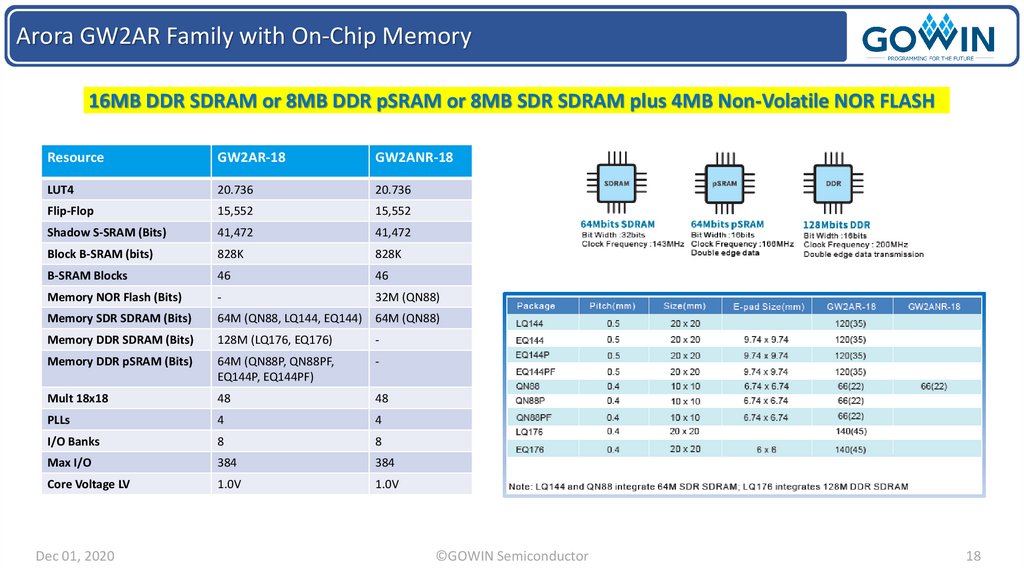
18.
Arora GW2AR Family with On-Chip Memory16MB DDR SDRAM or 8MB DDR pSRAM or 8MB SDR SDRAM plus 4MB Non-Volatile NOR FLASH
Resource
GW2AR-18
GW2ANR-18
LUT4
20.736
20.736
Flip-Flop
15,552
15,552
Shadow S-SRAM (Bits)
41,472
41,472
Block B-SRAM (bits)
828K
828K
B-SRAM Blocks
46
46
Memory NOR Flash (Bits)
-
32M (QN88)
Memory SDR SDRAM (Bits)
64M (QN88, LQ144, EQ144)
64M (QN88)
Memory DDR SDRAM (Bits)
128M (LQ176, EQ176)
-
Memory DDR pSRAM (Bits)
64M (QN88P, QN88PF,
EQ144P, EQ144PF)
-
Mult 18x18
48
48
PLLs
4
4
I/O Banks
8
8
Max I/O
384
384
Core Voltage LV
1.0V
1.0V
Dec 01, 2020
©GOWIN Semiconductor
.
18
19.
Arora GW2AN-18 with On-Chip Flash – Available Q1 2021Adds I2C Configuration, 2MB Non-Volatile NOR FLASH, Supports Background Updates & Programming
Resource
GW2AN-18
LUT4
20.736
Flip-Flop
15,552
Shadow S-SRAM (Bits)
41,472
Block B-SRAM (bits)
540K
B-SRAM Blocks
30
Memory NOR Flash (Bits)
2-bit streams
16Mb
Mult 18x18
48
PLLs
4
LVDS Bandwidth (per lane)
1.25Gbps
MIPI Bandwidth (per lane)
Adds I2C Programming Support
Supports 5 Configuration Modes
• JTAG, CPU, I2C, SSPI, SERIAL, Autoboot
Dual Partition NOR Flash
• Supports Autoboot (Non-volatile)
• Supports Background Updates & Programming
• Update & Switch Images while device is active
Package
Pitch (mm)
Size (mm)
GW2AN-18
1.2Gbps
PG256
1.0
17 x 17
206
I/O Banks
8
UG256
0.8
14 x 14
206
Max I/O
384
UG324
0.8
15 x 15
279
Core Voltage EV
1.0V
UG332
0.8
17 x 17
278
Core Voltage LV
1.2V
UG400
0.8
17 x 17
335
Core Voltage UV
2.5V / 3.3V
UG484
0.8
19 x 19
384
Dec 01, 2020
.
©GOWIN Semiconductor
19
20.
GW5AT 128K LUTs – Targeting 2021 ReleaseThird Generation, 22nm SRAM Technology, High-Speed Transceivers
GW5AT Features
Resource
GW5AT-128
LUT4
126.72K
Shadow S-SRAM (Bits)
1013.76K
Block B-SRAM (Total bits)
5400K
B-SRAM Blocks
300 x 18K
DSP
300 (27x18) or 300 (27x36)
or 600 (12x12)
PLLs
12
Transceivers 400Mbps to 12.5Gbps
8
PCIe 2.0/1.1 Hardcore
1, x1, x2, x4, x8 PCIe2.0
LVDS Bandwidth (per lane)
1.25Gbps
MIPI Bandwidth (per lane)
2.5Gbps
DDR3 Bandwidth
1.333Gbps
I/O Banks
6
Max I/O
Core Voltage Options
Dec 01, 2020
..
Third Generation High Density (22nm) RAM-based FPGA
Embedded Microcontroller
On-Chip Temperature and Voltage Sensors
New Architecture
New DSP 27x18, 27x36, 12x12 and 56-bit Accumulate
High Performance PLLs x12
16 Global Clocks
4 High-Speed Clocks per Bank
High-Speed Transceivers x8
10 Gigabit Ethernet
High Performance IO
Hardcore MIPI Interfaces 2.5Gbps
LVDS up to 1250 Mbps
DDR3 up to 1333 Mbps
Hardcore PCIe2.0/1.1 Hardcore
Supports x1, x2, x4, x8 Endpoint and Root Port
Support ECC correction in SRAM
Package
Pitch (mm)
Size (mm)
GW5A(T)
300
Flip-Chip BGA 484
1.0
23
285
1.2/1.35/1.5/1.8/2.5/3.3V
Flip-Chip BGA 676
1.0
27
300
©GOWIN Semiconductor
20
21.
GOWIN Product RoadmapDensity
LUTs
55nm
22nm
16/14/7nm
High Density
High performance;
500K
Communication, data center, cloud,
machine vision, autopilot, AI;
GW7AT
350K to 1000K
28Gbps SERDES
22nm 3rd Gen
Embedded high performance MCU;
GW5AT
120K to 350K
12Gbps SERDES
100K
14nm / 7nm 4th Gen
55nm 1st Generation
50K
GW2A-55
GW2AR-18
20K
18K
10K
GW1NR-4/9
4K
2014
Dec 01, 2020
GW1NS
GW1N-1/4/9
2015
2016
GW1NZ
2017
Industry, auto, surveillance, display,
AI edge, connectivity,
communication, commercial;
Embedded ARM M, R, A, or RISC-V
soft/hard IP core;
GW2AN-18
Low Density
55nm 1st Generation
9K
High performance/cost ratio, power
and speed medium;
GW2ANR-18
GW2A-18
1K
Mid Density
GW5A
20K to 100K
22nm
2018
2019
22nm
GW1NSE
GW1NRF
GW1N-2
2020
©GOWIN Semiconductor
2021
2nd
Non-volatile, low power, low cost;
Gen
Display, IoT, Wearable, audio, video,
connectivity, AI edge, security;
GW4N
1K to 9K
2022
Embedded ARM Cortex-M or RISC-V
hard or soft IP core;
2023
21
22.
GOWIN Website & Member RegistrationRegister as a Member to Access
Documents and Download Data
Member Login
Provides Unrestricted Access to
the GOWIN Website.
GOWIN Website
https://www.gowinsemi.com/
GOWIN Members Area
https://www.gowinsemi.com/en/member/
Dec 01, 2020
©GOWIN Semiconductor
22
23.
GOWIN Development ToolsGOWIN EDA Tool: FPGA Designer, Firmware Development
• DOWNLOAD GOWIN EDA – Latest Version Gowin®EDA_Gowin V1.9.5.01_win
Licensed by GOWIN
GOWIN MCU (Microcontroller Unit) Designer: ARM Cortex-M and RISC-V PicoRV32 Processor Software Development
• ARM DesignStart FPGA – GOWIN MCU Designer (Based on GNU GCC compilation and open-source Eclipse framework).
Licensed by GOWIN
ARM Keil: ARM Cortex-M processor Development: based on µVision (Windows only)
• ARM DesignStart FPGA – ARM Keil Webpage
Licensed by ARM, MDKLite is free but restricted to 32Kbytes Code Size
RISC-V N25 Core AndeSight RDS Eclipse-based IDE
• See DOWNLOAD GOWIN EDA – Dropbox for RISC-V-for-GW2A-Release package
Licensed by GOWIN
GOWIN SecureFPGA Package – to support GW1NSE family devices.
• DOWNLOAD GOWIN EDA – Gowin secureFPGA (IID and SHA3) SDK
Licensing N/A – Requires GOWIN MCU Designer, GOWIN EDA FPGA Designer
GOWIN GW1NRF Bluetooth BLE
• DOWNLOAD GOWIN EDA – GW1NRF SoC SDK V1.0 For Windows
Licensing N/A – Synopsys MetawareLite (freely licensed).
Dec 01, 2020
©GOWIN Semiconductor
23
24.
GOWIN EDA® FPGA DesignerEDA GUI
Command Line Interface
Operating System
• Windows or Linux (inc. Ubuntu)
Freely Licensed
• Fixed or Floating Licenses
Easy-of-Use
• Very Intuitive & Familiar Looking
Design Entry
Mixed language Support
VHDL, Verilog & System Verilog
HDL Input
Support for External
Third-Party Simulators
Simulation
GOWIN Synthesis
Synthesis
Standard .sdc format
Physical Constraints
Binary or Text
CRC, Compression & Security
Analyzer Oscilloscope
Real-Time Debug
Dec 01, 2020
Place & Route
Timing Constraints
Bitstream
Hardware Validation
©GOWIN Semiconductor
Fully Featured Tool Chain
• Free IP Core Generator
• Floor-Planner
• Timing Constraints Editor
• Schematic Viewer
• Hierarchy Viewer
• GOWIN Analyzer Oscilloscope
• Project Archiving
• Module Encryption
• Standalone Programmer
24
25.
GOWIN IP Core Examples (Newer Releases in Green)IP Cores - https://www.gowinsemi.com/en/support/ip/
RISC-V Core
SPMI Master & Slave
SDIO / SPI Bridge
DDR/DDR2/DDR3* Controller
CAN Bus Controller
USB1.1
PCI Controller
AHB Bus Arbiter
Video Frame pSRAM Buffer
pSRAM Controller
SDIO Slave Controller
PCI to CAN Bridge
SDRAM Controller
Video Scaler
SPI NOR Flash Controller
I3C Master & Slave
Colour Space Conversion
FOC Current Loop Control
MIPI-TX-D-PHY
Flash Controller
HyperRAM Memory Interface
MIPI-RX-D-PHY
SPDIF
DVI RX/TX
FIFO/FIFO_SC
CORDIC
Digital Frequency Synthesizer
RAM-Based-Shift-Registers
Adaptive Filters
I2C / UART Bridge
DSP Modules
FFT
SPI / UART Bridge
BSRAM Modules
7:1 LCD Controller
Audio Sample Rate Converter
Clock Modules
XCORR
Wishbone Bridge
PDM2PCM
USB1.1
Dec 01, 2020
©GOWIN Semiconductor
Reference Design Examples
Audio Sample Rate Converter (ASRC)
DDR3 Memory Interface
FFT
I2C/SPI/UART
7:1 LVDS RX
1:4 mini LVDS TX
USB 1.0 / 1.1
DVI TX/RX
25
26.
GOWIN GoAI 2.0 Machine Learning (ML)Targets Low Cost, Low Power, Edge AI Applications
Deploy Machine Learning models on GOWIN FPGA
Based on established Tensorflow Framework
Up to 80x faster than equivalent standalone microcontrollers
GOWIN GoAI 2.0
Market Positioning
1) Training Framework
Tensorflow / Keras
2) Testing
Tensorflow / Keras
3) Optimization
Tensorflow Lite / Keras
4) GoAI 2.0 Assembler
FPGA Bitstream
Model Coefficients
MCU Firmware
5) Deployment
GOWIN Programmer
Dec 01, 2020
©GOWIN Semiconductor
26
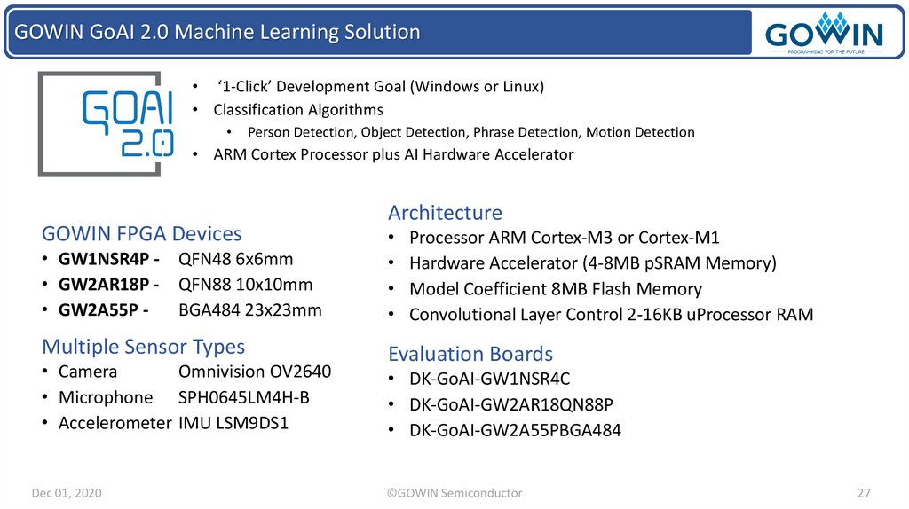
27.
GOWIN GoAI 2.0 Machine Learning Solution• ‘1-Click’ Development Goal (Windows or Linux)
• Classification Algorithms
Person Detection, Object Detection, Phrase Detection, Motion Detection
• ARM Cortex Processor plus AI Hardware Accelerator
GOWIN FPGA Devices
Architecture
• GW1NSR4P - QFN48 6x6mm
• GW2AR18P - QFN88 10x10mm
• GW2A55P BGA484 23x23mm
Multiple Sensor Types
Evaluation Boards
• Camera
Omnivision OV2640
• Microphone SPH0645LM4H-B
• Accelerometer IMU LSM9DS1
Dec 01, 2020
Processor ARM Cortex-M3 or Cortex-M1
Hardware Accelerator (4-8MB pSRAM Memory)
Model Coefficient 8MB Flash Memory
Convolutional Layer Control 2-16KB uProcessor RAM
• DK-GoAI-GW1NSR4C
• DK-GoAI-GW2AR18QN88P
• DK-GoAI-GW2A55PBGA484
©GOWIN Semiconductor
27
28.
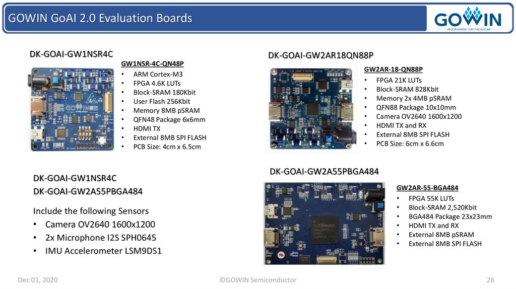
GOWIN GoAI 2.0 Evaluation BoardsDK-GOAI-GW1NSR4C
GW1NSR-4C-QN48P
• ARM Cortex-M3
• FPGA 4.6K LUTs
• Block-SRAM 180Kbit
• User Flash 256Kbit
• Memory 8MB pSRAM
• QFN48 Package 6x6mm
• HDMI TX
• External 8MB SPI FLASH
• PCB Size: 4cm x 6.5cm
DK-GOAI-GW1NSR4C
DK-GOAI-GW2A55PBGA484
DK-GOAI-GW2AR18QN88P
GW2AR-18-QN88P
• FPGA 21K LUTs
• Block-SRAM 828Kbit
• Memory 2x 4MB pSRAM
• QFN88 Package 10x10mm
• Camera OV2640 1600x1200
• HDMI TX and RX
• External 8MB SPI FLASH
• PCB Size: 6cm x 6.6cm
DK-GOAI-GW2A55PBGA484
GW2AR-55-BGA484
• FPGA 55K LUTs
• Block-SRAM 2,520Kbit
• BGA484 Package 23x23mm
• HDMI TX and RX
• External 8MB pSRAM
• External 8MB SPI FLASH
Include the following Sensors
• Camera OV2640 1600x1200
• 2x Microphone I2S SPH0645
• IMU Accelerometer LSM9DS1
Dec 01, 2020
©GOWIN Semiconductor
28
29.
LittleBee GW1NRF Bluetooth Development KitGW1NRF Eval Board
• GW1NRF Single Package Bluetooth 5.0 Low Energy IC Device.
• FCC / SIG Certified Bluetooth 5.0 Low Energy Module.
• Example Application Code.
DK-BLE-CEIT-ASSEM
Bluetooth Low Energy Module
Dec 01, 2020
©GOWIN Semiconductor
29
30.
LittleBee GW1N Development BoardsDK-START-GW1NZ
DK-START-GW1N4
GW1NZ Eval Board
• GW1NZ-LV1FN32
• GW1NZ-ZV1FN32
• LVDS
• GPIO
DK-START-GW1N1
GW1N-4 Eval Board
• GW1N-LV4/4B LQ144
• LVDS
• GPIO
• Serial Flash
GW1NR-4 Eval Board
• GW1NR-LV4MG81P
• 64Mbits pSRAM
• GPIO
DK-START-GW1NR9
DK-START-GW1N9
GW1N-1 Eval Board
• GW1N-LV1LQ144
• LVDS
• GPIO
Dec 01, 2020
DK-START-GW1NR4
GW1N-9 Eval Board
• GW1N-LV9LQ144
• LVDS
• GPIO
• Serial Flash
©GOWIN Semiconductor
GW1NR-9 Eval Board
• GW1NR-LV9LQ144P
• 64Mbits pSRAM
• LVDS / MIPI
• GPIO
30
31.
LittleBee GW1NS µSoC Development BoardsDK-START-GW1NS2
DK-START-GW1NSR2
GW1NSR-2 Eval Board
• GW1NSR-LX2CQN48P
• ARM Cortex-M3
• 32Mbits pSRAM
• LVDS
• GPIO
GW1NS-2 Eval Board
• GW1NS-UX2CLQ144
• ARM Cortex-M3
• LVDS
• GPIO
DK-START-GW1NS4-QN48
GW1NS-4 Eval Board
• GW1NS-LV4CQN48
• ARM Cortex-M3
• LVDS
• GPIO
Dec 01, 2020
DK-START-GW1NSR4-QN48
GW1NSR-4 Eval Board
• GW1NSR-LV4CQN48
• ARM Cortex-M3
• 64Mbits pSRAM
• LVDS
• GPIO
©GOWIN Semiconductor
DK-START-GW1NSER4-QN48
GW1NSER-4 SecureFPGA
• GW1NSR-LV4CQN48
• ARM Cortex-M3
• 64Mbits pSRAM
• LVDS
• GPIO
31
32.
Arora GW2A Development BoardsDK-START-GW2A18
DK-START-GW2AR18
GW2A-18 Eval Board
• GW2A-LV18PG256
• 2GB DDR3 External Memory
• Gigabit Ethernet x2
• LVDS TX / RX
• SD Card
• External Flash
GW2AR-18 Eval Board
• GW2A-LV18EQ144
• 64Mb pSRAM On-Chip
• Ethernet x2
• LVDS TX / RX
• External Flash
DK-START-GW2A55-PG484
DK-VIDEO-GW2A18-PG484
GW2A-18 Video Board
• GW2A-LV18PG484
• 2GB DDR3 External Memory
• HDMI RX x2
• HDMI TX x2
• MIPI CSI / DSI
• LVDS TX / RX
• SD Card
• External Flash
Dec 01, 2020
©GOWIN Semiconductor
GW2A-55 Eval Board
• GW2A-LV55PG484
• 2GB DDR3 External Memory
• Gigabit Ethernet x2
• LVDS TX / RX
• SD Card
• CAN Bus
• MIPI CSI / DSI
• RTC Module
• External Flash
32