
 Инженерная графика
1874 - Semiconductor Point-Contact Rectifier Effect Discovered
1.
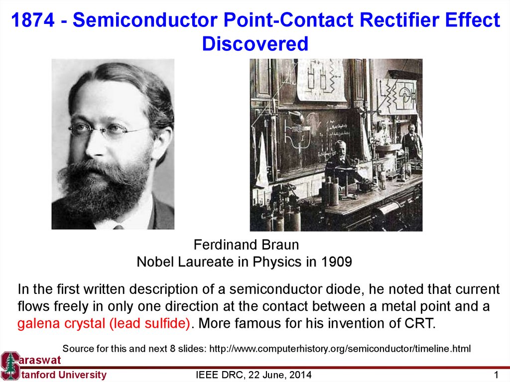
1874 - Semiconductor Point-Contact Rectifier EffectDiscovered
Ferdinand Braun
Nobel Laureate in Physics in 1909
In the first written description of a semiconductor diode, he noted that current
flows freely in only one direction at the contact between a metal point and a
galena crystal (lead sulfide). More famous for his invention of CRT.
Source for this and next 8 slides: http://www.computerhistory.org/semiconductor/timeline.html
araswat
tanford University
IEEE DRC, 22 June, 2014
1
2.
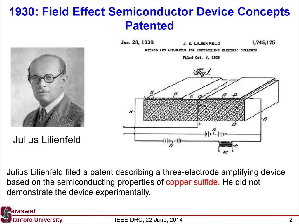
1930: Field Effect Semiconductor Device ConceptsPatented
Julius Lilienfeld
Julius Lilienfeld filed a patent describing a three-electrode amplifying device
based on the semiconducting properties of copper sulfide. He did not
demonstrate the device experimentally.
araswat
tanford University
IEEE DRC, 22 June, 2014
2
3.
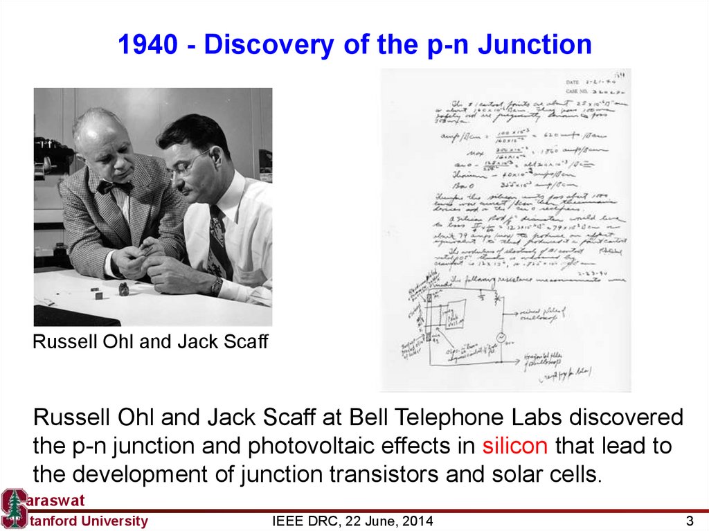
1940 - Discovery of the p-n JunctionRussell Ohl and Jack Scaff
Russell Ohl and Jack Scaff at Bell Telephone Labs discovered
the p-n junction and photovoltaic effects in silicon that lead to
the development of junction transistors and solar cells.
araswat
tanford University
IEEE DRC, 22 June, 2014
3
4.
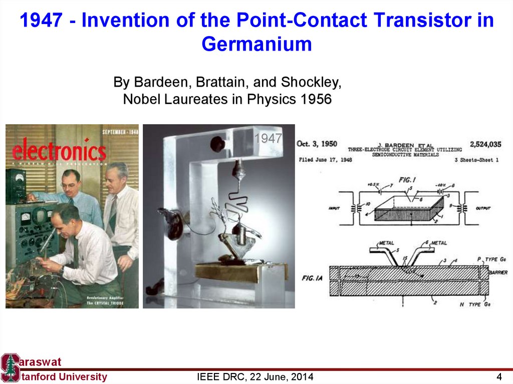
1947 - Invention of the Point-Contact Transistor inGermanium
By Bardeen, Brattain, and Shockley,
Nobel Laureates in Physics 1956
1947
araswat
tanford University
IEEE DRC, 22 June, 2014
4
5.
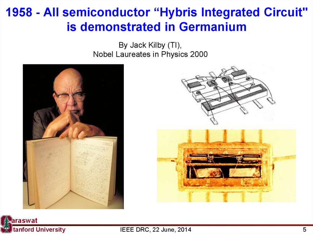
1958 - All semiconductor “Hybris Integrated Circuit"is demonstrated in Germanium
By Jack Kilby (TI),
Nobel Laureates in Physics 2000
araswat
tanford University
IEEE DRC, 22 June, 2014
5
6.
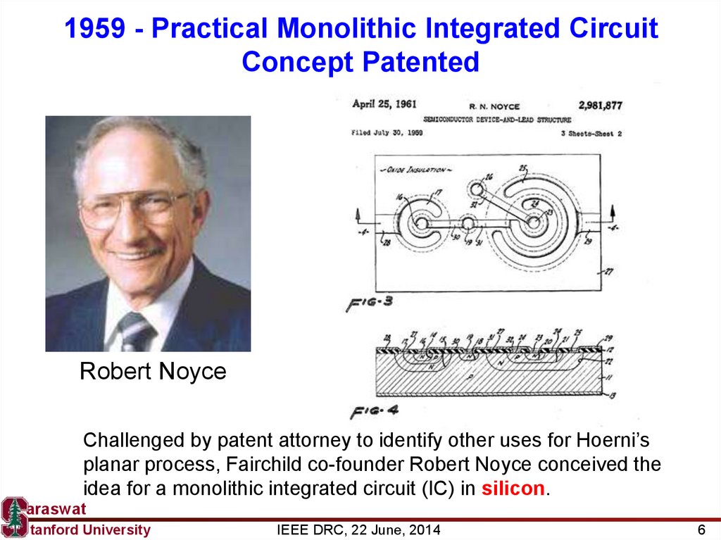
1959 - Practical Monolithic Integrated CircuitConcept Patented
Robert Noyce
Challenged by patent attorney to identify other uses for Hoerni’s
planar process, Fairchild co-founder Robert Noyce conceived the
idea for a monolithic integrated circuit (IC) in silicon.
araswat
tanford University
IEEE DRC, 22 June, 2014
6
7.
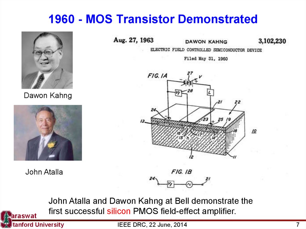
1960 - MOS Transistor DemonstratedDawon Kahng
John Atalla
araswat
John Atalla and Dawon Kahng at Bell demonstrate the
first successful silicon PMOS field-effect amplifier.
tanford University
IEEE DRC, 22 June, 2014
7
8.
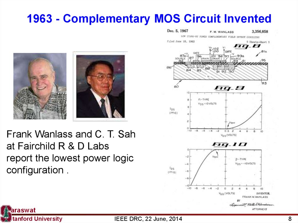
1963 - Complementary MOS Circuit InventedFrank Wanlass and C. T. Sah
at Fairchild R & D Labs
report the lowest power logic
configuration .
araswat
tanford University
IEEE DRC, 22 June, 2014
8
9.
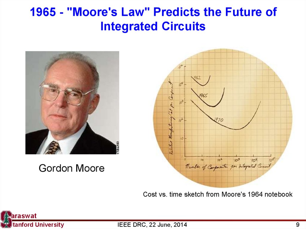
1965 - "Moore's Law" Predicts the Future ofIntegrated Circuits
Gordon Moore
Electronics Magazine (April 1965)
IEEE, IEDM (1975)
Cost vs. time sketch from Moore's 1964 notebook
araswat
tanford University
IEEE DRC, 22 June, 2014
9
10.
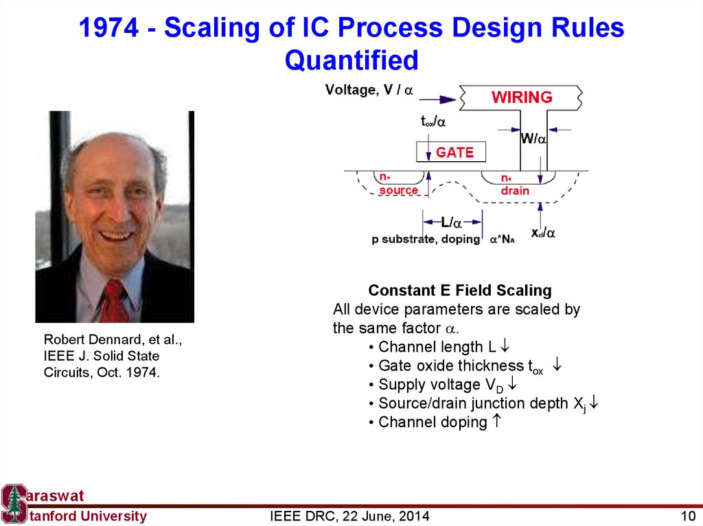
1974 - Scaling of IC Process Design RulesQuantified
Robert Dennard, et al.,
IEEE J. Solid State
Circuits, Oct. 1974.
Constant E Field Scaling
All device parameters are scaled by
the same factor .
• Channel length L
• Gate oxide thickness tox
• Supply voltage VD
• Source/drain junction depth Xj
• Channel doping
araswat
tanford University
IEEE DRC, 22 June, 2014
10
11.
Thank youaraswat
tanford University
IEEE DRC, 22 June, 2014
11