Похожие презентации:
Design and technology of flexible electronic components
1.
DESIGN AND TECHNOLOGYOF FLEXIBLE ELECTRONIC
COMPONENTS
2.
FLEXIBLE ELECTRONICS30 years of commercialization
North Europe
• Finland (VTT, TactoTec, Canatu)
• Belgium/Netherlands (Imec, Holst Center)
• Great Britian (PragmatIC, Flexnable)
USA
• E-ink
• Amazon Go
• Thin Film
Russia
• Technospark
South East Asia
• Japan (Sharp, INOEL)
• South Korea (LG Displays, Samsung)
• Taiwan (Foxconn)
• Taiwan (Giantplus)
• China (BOE)
2
3.
FLEXIBLE ELECTRONICSpattern breaking
Large Area Electronics
«Fab-in-box»
Electronics produced in meters
Microelectronic mini-fab
manufacturing unit in a corner
of your factory (3D printing
development model)
3
4.
PRODUCTION FACILITIES (midsize scale)TFT matrices and plastic ICs
PRODUCTION
FAB
EQUIPMENT
Gen 2,5
4 183 sq m
41 pcs
Substrate size
FAB size
Equipment units
4 000 sq m TFT
Including
Per annum
IGZO TFT • OTFT
Technology
1800 sq m
Clean room
World-class
equipment
for
the
production of flat panel displays and an
innovative process for the production of
plastic-based TFT matrices.
TECHNOLOGY PARTNERS
4
5.
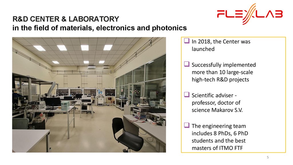
R&D CENTER & LABORATORYin the field of materials, electronics and photonics
❑ In 2018, the Center was
launched
❑ Successfully implemented
more than 10 large-scale
high-tech R&D projects
❑ Scientific adviser professor, doctor of
science Makarov S.V.
❑ The engineering team
includes 8 PhDs, 6 PhD
students and the best
masters of ITMO FTF
5
6.
TECHNOLOGICAL DOMAINSFlexible (frost-resistant) EPD
2022-2024
Flexible OLED
Optical sensors, X-ray scanners
Energy harvesting
ID tags: Flex ID (optical) / RFID / NFC
Smart window / AR
2024-2026
Smart LED optics
Microfluidic sensors
Flexible non-volatile memory
6
7.
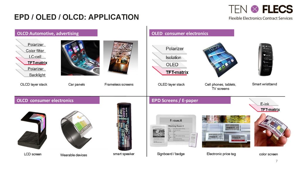
EPD / OLED / OLCD: APPLICATIONOLCD Automotive, advertising
OLCD layer stack
Car panels
OLED consumer electronics
Frameless screens
Wearable devices
Cell phones, tablets,
TV screens
Smart wristband
Electronic price tag
color screen
EPD Screens / E-paper
OLCD consumer electronics
LCD screen
OLED layer stack
smart speaker
Signboard / badge
7
8.
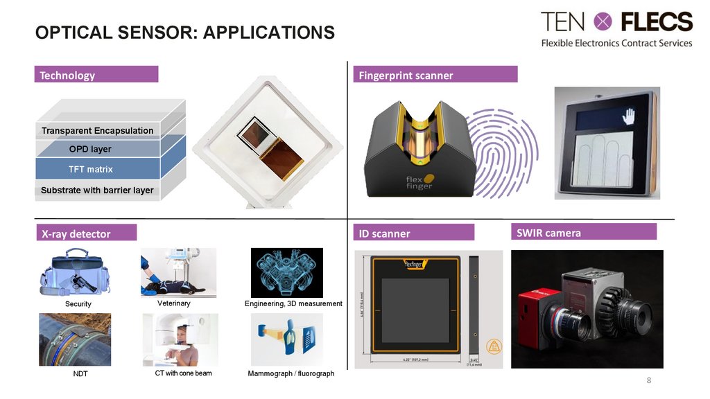
OPTICAL SENSOR: APPLICATIONSTechnology
Fingerprint scanner
Transparent Encapsulation
OPD layer
TFT matrix
Substrate with barrier layer
ID scanner
X-ray detector
Security
NDT
Veterinary
Engineering, 3D measurement
CT with cone beam
Mammograph / fluorograph
SWIR camera
8
9.
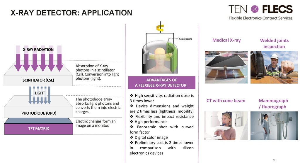
X-RAY DETECTOR: APPLICATIONMedical X-ray
Welded joints
inspection
CT with cone beam
Mammograph
/ fluorograph
X-RAY RADIATION
SCINTILATOR (CSL)
Absorption of X-ray
photons in a scintillator
(Csl). Conversion into light
photons (light).
LIGHT
PHOTODIODE (OPD)
TFT MATRIX
The photodiode array
absorbs light photons and
converts them into electric
charges.
Electric charges form an
image on a monitor.
ADVANTAGES OF
A FLEXIBLE X-RAY DETECTOR :
❖ High sensitivity, radiation dose is
3 times lower
❖ Device dimensions and weight
are 2 times less (lightness, mobility)
❖ Flexibility and impact resistance
❖ High performance
❖ Panoramic shot with curved
form factor
❖ Digital color image
❖ Preliminary cost is 2 times lower
in
comparison
with
silicon
electronics devices
9
10.
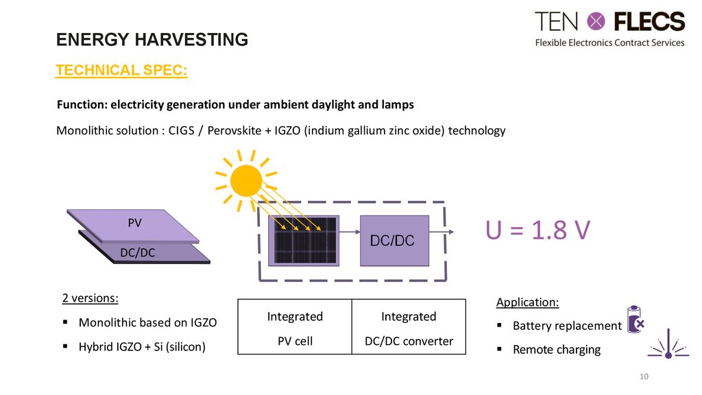
ENERGY HARVESTINGTECHNICAL SPEC:
Function: electricity generation under ambient daylight and lamps
Monolithic solution : CIGS / Perovskite + IGZO (indium gallium zinc oxide) technology
PV
U = 1.8 V
DC/DC
2 versions:
Application:
▪ Monolithic based on IGZO
Integrated
Integrated
▪ Hybrid IGZO + Si (silicon)
PV cell
DC/DC converter
▪ Battery replacement
▪ Remote charging
10
11.
HARVESTER: APPLICATIONSMART HOUSE
Smart devices, switches
and light sensors, control
panels
MEDICINE
Health monitoring,
pacemakers
SECURITY
Smart cameras, motion
sensors, smart alarm,
perimeter trackers
ADVANTAGES
Operation from low-intensity
radiation sources
Low cost
Increased reliability
Miniaturization: thin, light
Flexible, impact resistant.
High conversion efficiency
WEARABLE
ELECTRONICS
Smart watches and
bracelets, smart clothes,
headphones
RETAIL
INDUSTRY
Electronic price tags,
smart thermometers,
humidity sensors
All modern sensors,
including smoke
detectors, air pollution
Full-fledged replacement of chemical
energy sources for a range of equipment
11
12.
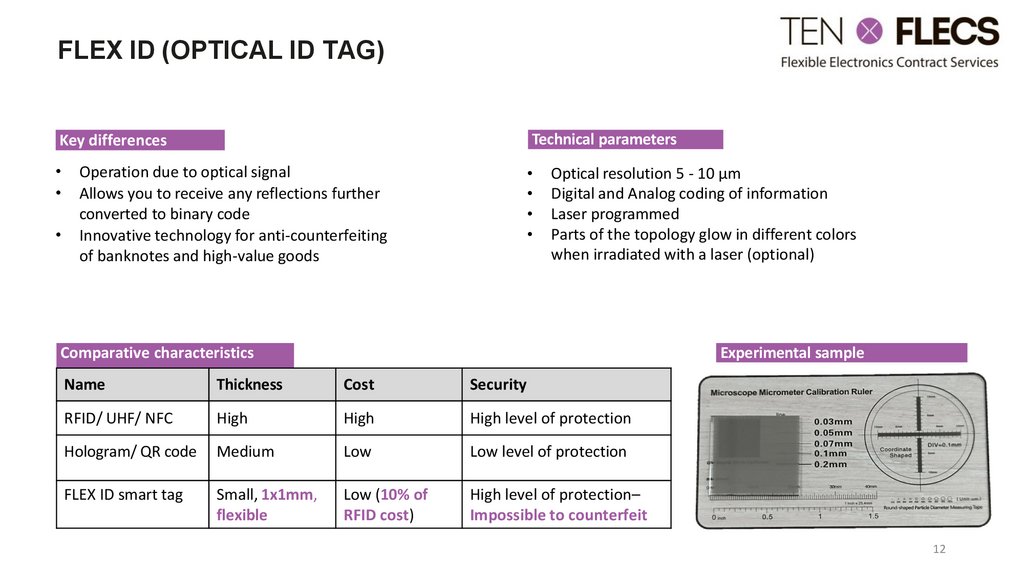
FLEX ID (OPTICAL ID TAG)Key differences
Technical parameters
Operation due to optical signal
Allows you to receive any reflections further
converted to binary code
Innovative technology for anti-counterfeiting
of banknotes and high-value goods
Optical resolution 5 - 10 µm
Digital and Analog coding of information
Laser programmed
Parts of the topology glow in different colors
when irradiated with a laser (optional)
Experimental sample
Comparative characteristics
Name
Thickness
Cost
Security
RFID/ UHF/ NFC
High
High
High level of protection
Hologram/ QR code
Medium
Low
Low level of protection
FLEX ID smart tag
Small, 1х1mm,
flexible
Low (10% of
RFID cost)
High level of protection–
Impossible to counterfeit
12
13.
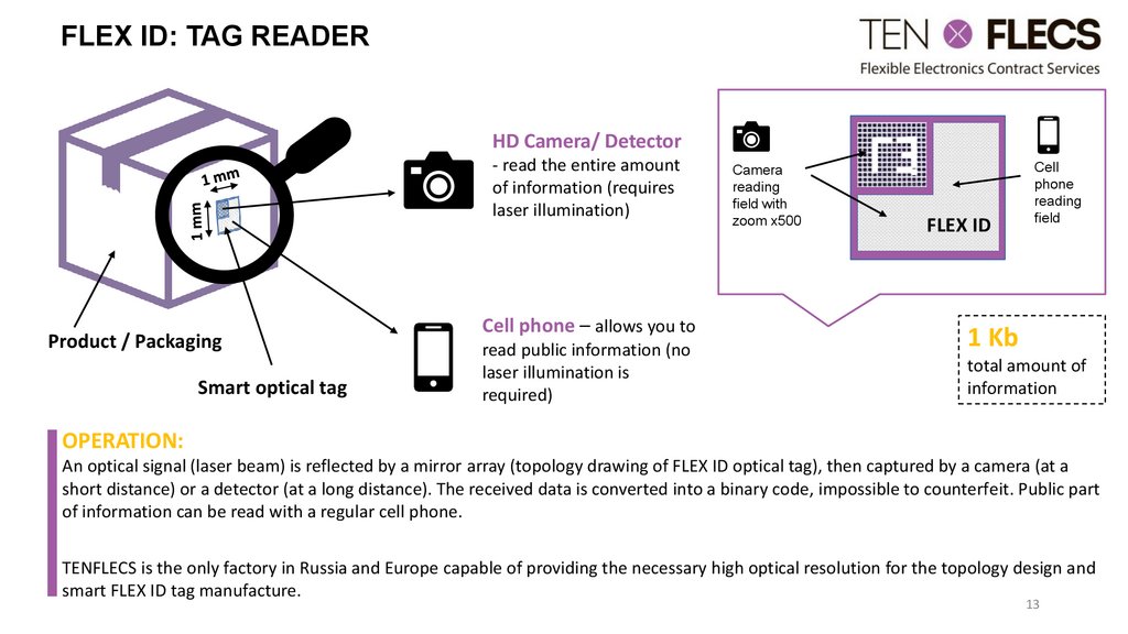
FLEX ID: TAG READERHD Camera/ Detector
- read the entire amount
of information (requires
laser illumination)
Product / Packaging
Smart optical tag
Cell phone – allows you to
read public information (no
laser illumination is
required)
Camera
reading
field with
zoom x500
FLEX ID
Cell
phone
reading
field
1 Kb
total amount of
information
OPERATION:
An optical signal (laser beam) is reflected by a mirror array (topology drawing of FLEX ID optical tag), then captured by a camera (at a
short distance) or a detector (at a long distance). The received data is converted into a binary code, impossible to counterfeit. Public part
of information can be read with a regular cell phone.
TENFLECS is the only factory in Russia and Europe capable of providing the necessary high optical resolution for the topology design and
smart FLEX ID tag manufacture.
13
14.
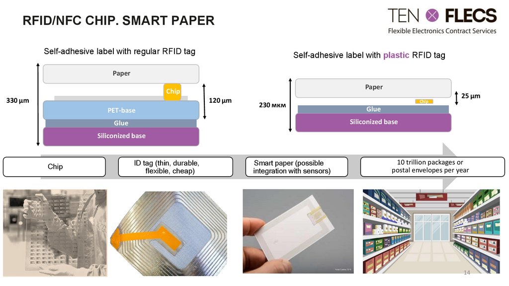
RFID/NFC CHIP. SMART PAPERSelf-adhesive label with regular RFID tag
Self-adhesive label with plastic RFID tag
Paper
Paper
Chip
330 µm
120 µm
PET-base
230 мкм
Chip
25 µm
Glue
Siliconized base
Glue
Siliconized base
Chip
ID tag (thin, durable,
flexible, cheap)
Smart paper (possible
integration with sensors)
10 trillion packages or
postal envelopes per year
14
15.
SMART DIMMING FILM (SMART WINDOW)- A thin and flexible film. Dimming level depends on the applied voltage.
- In the initial state, at zero voltage on the LC cell, light is maximally absorbed.
- When the voltage is turned on, the film goes into a state in which all dye molecules are oriented vertically, and the
incident light passes freely.
TECHNICAL SPEC:
Thickness ~100 µm
No blue/magenta tone and no hazy effect
Fast transition from transparent to opaque or intermediate state
Continuous dimming tuning is possible
Different spectrum and deep light modulation are possible due
to the variation of LC mixture
For LC cells a regular tech. process is applied
Bending radius of dimming films is ~ 100 mm
LC cells retain their integrity and functionality when bent
Dimming modes (light transmission):
• Light – 50%
• Dark – 10%
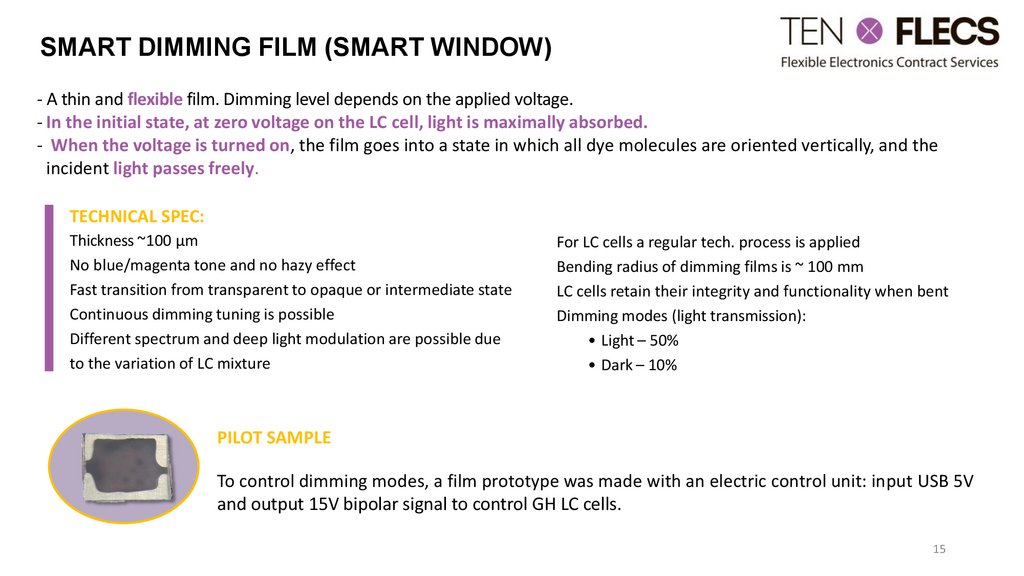
PILOT SAMPLE
To control dimming modes, a film prototype was made with an electric control unit: input USB 5V
and output 15V bipolar signal to control GH LC cells.
15
16.
This presentation is subject to copyright laws.Each reproduction or further transfer, as well as
extracts from the submitted document to a third
party, requires the written consent of the
TENFLECS company
https://tenflecs.com/
Alexandra Okhapkina
Senior sales manager
cell: +7 (909) 975 0717
email: ao@tenflecs.com
16





 Электроника


