Похожие презентации:
МЭМС и НЭМС: электронные системы, жидкостные вентили, насосы и биомедицинские системы
1. Наномеханика Nanomechanics of materials and systems
Лекции 15МЭМС и НЭМС:
электронные системы, жидкостные
вентили, насосы и биомедицинские
системы
MEMS and NEMS electronic systems fluid
valves, pumps and biomedical systems
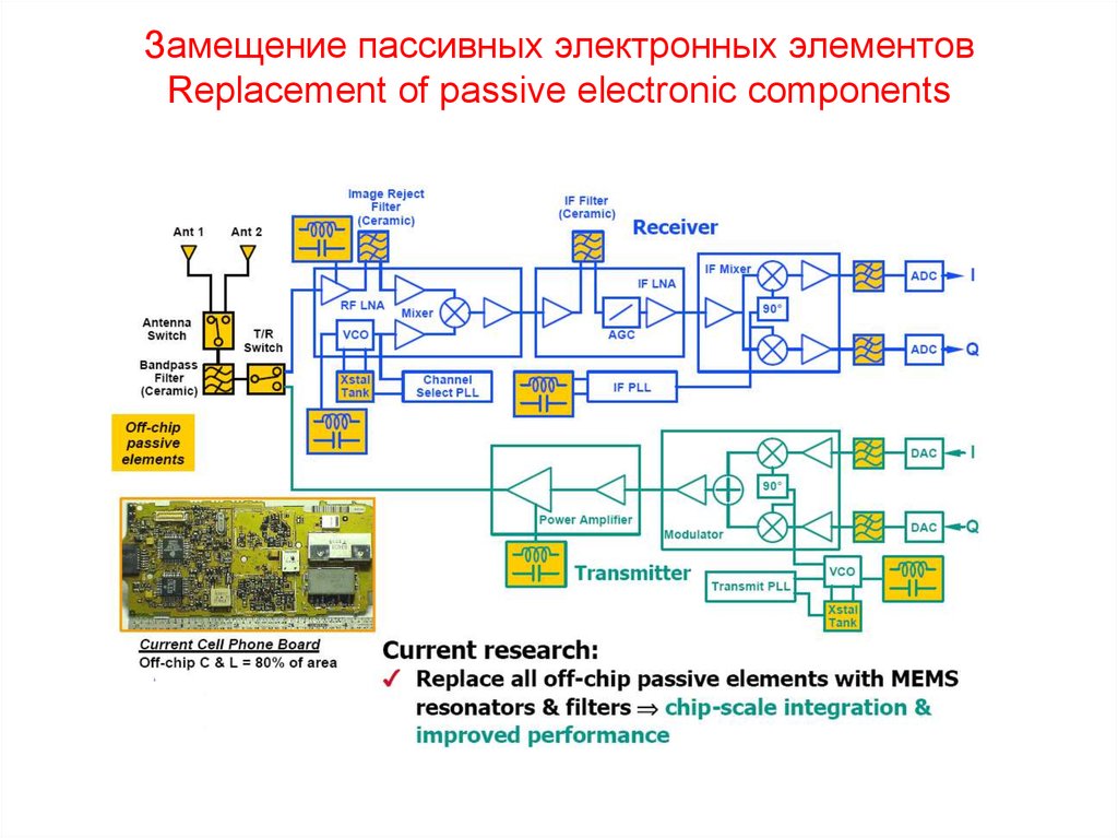
2. Замещение пассивных электронных элементов Replacement of passive electronic components
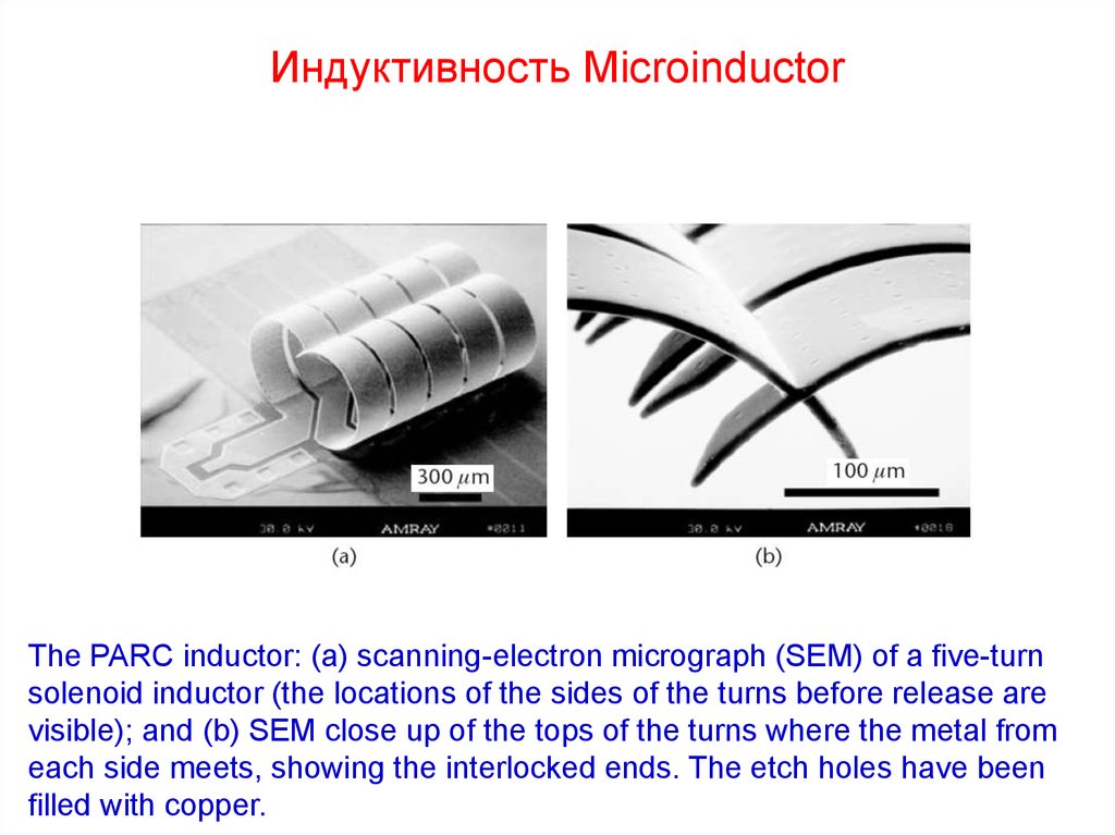
3. Индуктивность Microinductor
The PARC inductor: (a) scanning-electron micrograph (SEM) of a five-turnsolenoid inductor (the locations of the sides of the turns before release are
visible); and (b) SEM close up of the tops of the turns where the metal from
each side meets, showing the interlocked ends. The etch holes have been
filled with copper.
4. Индуктивность - последовательность производства НЭМС Fabrication of microinductor
5. Переменная емкость Tunable capacitor
6. Резонатор Resonator
Добротность Qкварц Q≈10000
RLC Q<1000
НЭМС:
вакуум Q>50000
воздух Q<50
k = E t (w/L)3
E = 160 GPa
t = 2 μm
w = 2 μm
L = 33 μm
m = 5.7 10-11 kg
f = 190 kHz
Illustration of a micromachined folded-beam comb-drive resonator. The left comb drive actuates the
device at a variable frequency ω. The right capacitive-sense-comb structure measures the
corresponding displacement by turning the varying capacitance into a current, which generates a
voltage across the output resistor. There is a peak in displacement, current, and output voltage at
the resonant frequency.
7. Высокочастотный резонатор с термокомпенсацией Resonator with thermal compensation
Illustration of the compensation scheme to reduce sensitivity in a resonant structure to temperature.A voltage applied to a top metal electrode modifies through electrostatic attraction the effective
spring constant of the resonant beam. Temperature changes cause the metal electrode to move
relative to the polysilicon resonant beam, thus changing the gap between the two layers. This
reduces the electrically induced spring constant opposing the mechanical spring while the
mechanical spring constant itself is falling, resulting in their combination varying much less with
temperature. (a) Perspective view of the structure, and (b) scanning electron micrograph of the
device. (Courtesy of: Discera, Inc., Ann Arbor, Michigan, USA.)
8. Переключатель Electric switch
Shock tolerance of30,000G,
insertion loss of
0.2 dB over 24–40 GHz,
open isolation of
40 dB,
lifetime of
1011 cycles,
cold-switched power of
1-W
MicroAssembly Technologies of Richmond, California, USA
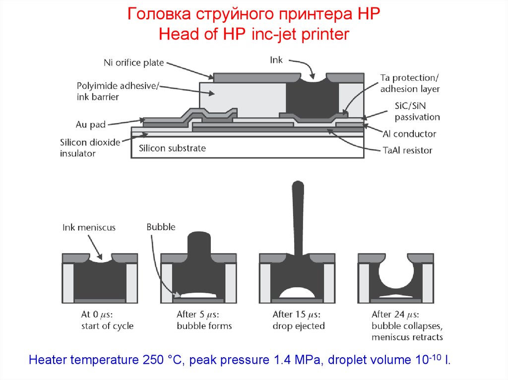
9. Головка струйного принтера HP Head of HP inc-jet printer
Heater temperature 250 °C, peak pressure 1.4 MPa, droplet volume 10-10 l.10. Головка струйного принтера HP - последовательность производства. Head of HP inc-jet printer - production steps
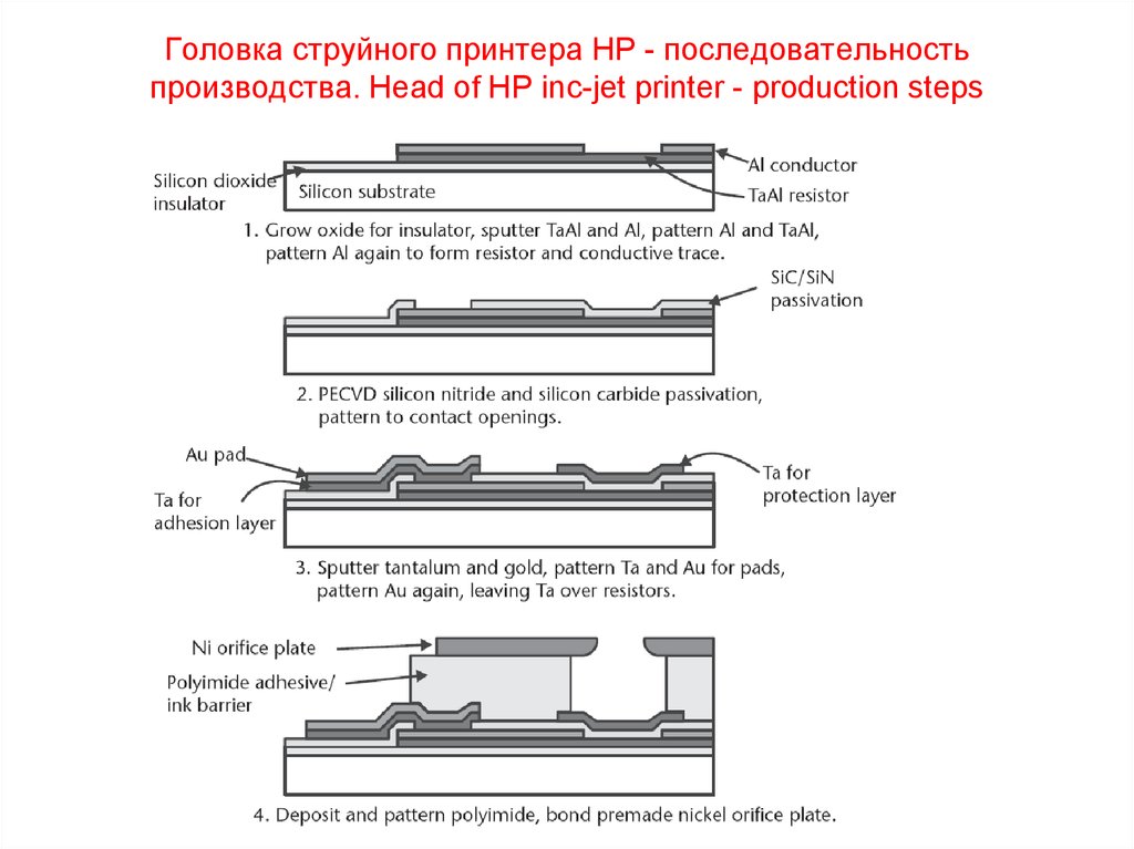
11. Головка струйного принтера HP
.Регуляторы потоков. MicrovalvesОбласти применения:
• Electronic flow regulation of refrigerant for increased energy
savings;
• Electronically programmable gas cooking stoves;
• Electronically programmable pressure regulators for gas
cylinders;
• Accurate mass flow controllers for high-purity gas delivery
systems;
• Accurate drug delivery systems;
• Control of fluid flow in portable biochemical analysis systems;
• Portable gas chromatography systems;
• Proportional control for electrohydraulic braking (EHB)
systems.
12. .Регуляторы потоков. Microvalves
Нормально-открытый регулятор потокаNormally open microvalve
Illustration of a normally open valve from Redwood Microsystems, Ca.
Heating of a control liquid sealed inside a cavity causes a thin silicon
diaphragm to flex and block the flow through the outlet orifice. The inlet
port is not shown.
The flow rate ranges from 0.1 sccm up to 1,500 sccm. The maximum inlet supply pressure is 690 kPa, the
switching time is typically 0.5s, and the corresponding average power consumption is 500 mW.
13. Нормально-открытый регулятор потока Normally open microvalve
Нормально-закрытый регулятор потокаNormally closed microvalve
Illustration of the basic operating mechanism of a normally closed
micromachined valve from Redwood Microsystems. (a) The upper stage of
the valve normally blocks fluid flow through the outlet orifice. The inlet orifice
is not shown. (b) Heating of the Fluorinert liquid sealed inside a cavity flexes
a thin silicon diaphragm which in turn causes a mechanical lever to lift the
valve plug.
14. Нормально-закрытый регулятор потока Normally closed microvalve
Ограничения регулятора потока с термопневматическим приводомУтечка тепла Leak of heat
Скорость переключения Switching time
Предельное давление Pressure limit
Влияние температуры окружающей среды
Ambient temperature dependence
• Влияние давления протекающей жидкости
Pressure of liquid flow
• Коррозия Corrosion
15. Ограничения регулятора потока с термо-пневматическим приводом
Микроклапан с приводом из металла с памятью формыNormally closed valve with shape-memory-alloy actuator
Assembly of the micromachined, normally closed valve with TiNi alloy actuator. The
beryllium-copper spring pushes a sapphire ball against the silicon poppet to close
the flow orifice. Resistive heating of the TiNi spring above its transition temperature
causes it to recover its original flat (undeflected) shape. The actuation pulls the
poppet away from the orifice, hence permitting fluid flow. (After: A. D. Johnson, TiNi
Alloy Company of San Leandro, California.)
16. Микроклапан с приводом из металла с памятью формы Normally closed valve with shape-memory-alloy actuator
Микроклапан – последовательность изготовления приводаNormally closed valve with TiN actuator – production steps
The valve consumes less than 200 mW and switches on in about 10 ms and off in
about 15 ms. The maximum gas flow rate and inlet pressure are 1,000 sccm and
690 kPa (100 psig), respectively. The valve measures 8 mm × 5 mm × 2 mm and
is assembled inside a plastic package. The list price for one valve is about $200.
17. Микроклапан – последовательность изготовления привода Normally closed valve with TiN actuator – production steps
Микронасос MicropumpIllustration of a cutout of a silicon micropump from the Fraunhofer Institute for Solid State
Technology of Munich, Germany. The overall device measures 7 x 7 x 2 mm3. The electrostatic
actuation of a thin diaphragm modulates the volume inside a chamber. An increase in volume
draws liquid through the inlet check valve. Relaxation of the diaphragm expels the liquid through
the outlet check valve. The pump rate initially rises with frequency and reaches a peak flow rate of 800
μl/min at 1 kHz.
18. Микронасос Micropump
Микронасос - последовательностьпроизводства НЭМС
19. Микронасос - последовательность производства НЭМС
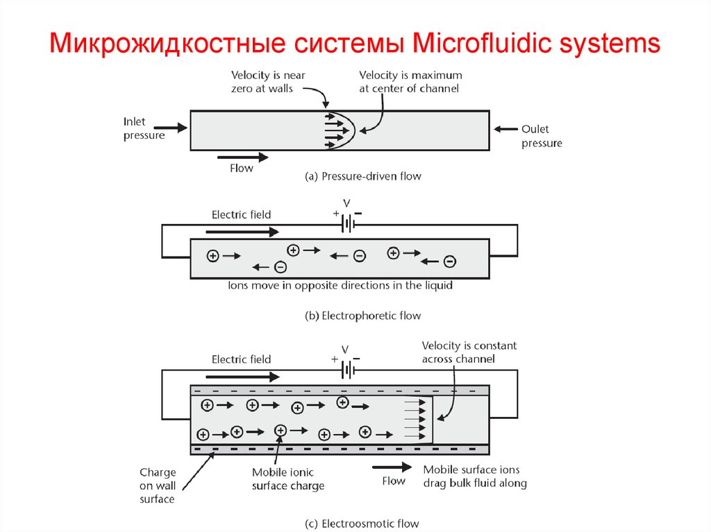
Микрожидкостные системы Microfluidic systems20. Микрожидкостные системы Microfluidic systems
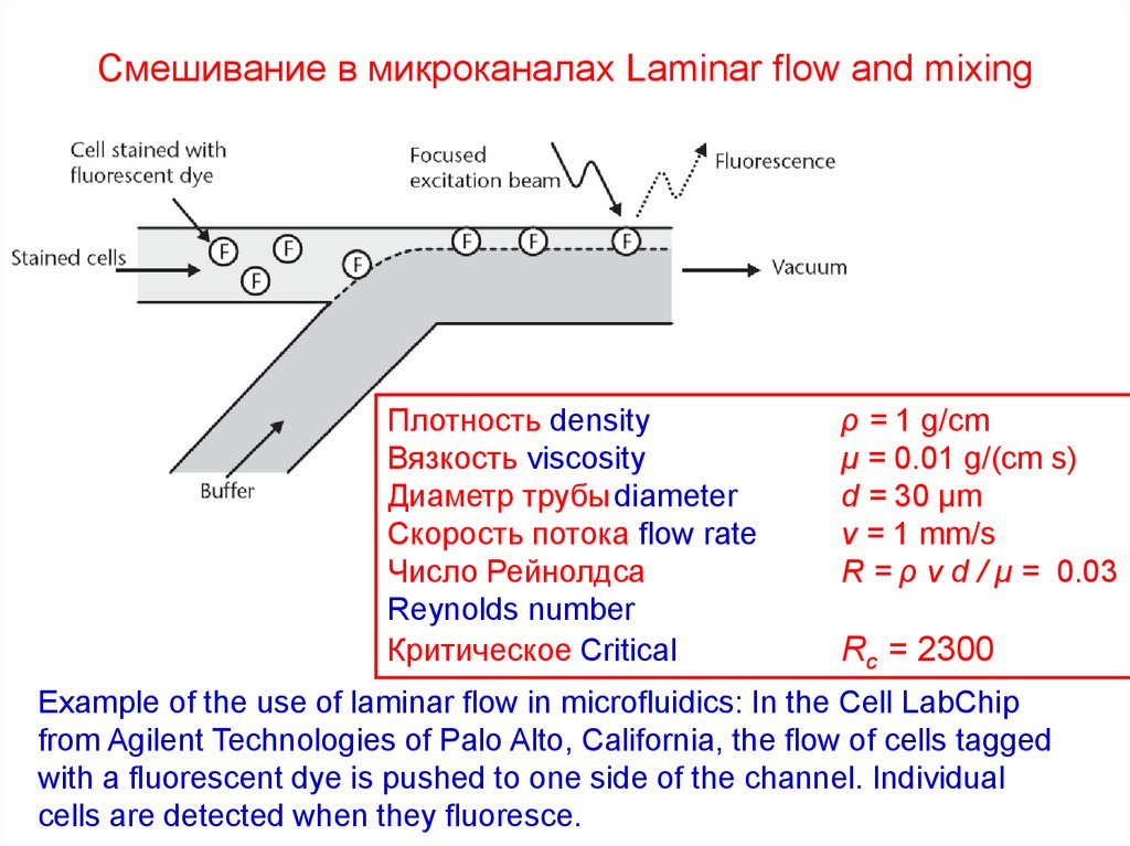
Смешивание в микроканалах Laminar flow and mixingПлотность density
Вязкость viscosity
Диаметр трубы diameter
Скорость потока flow rate
Число Рейнолдса
Reynolds number
Критическое Critical
ρ = 1 g/cm
μ = 0.01 g/(cm s)
d = 30 μm
v = 1 mm/s
R = ρ v d / μ = 0.03
Rс = 2300
Example of the use of laminar flow in microfluidics: In the Cell LabChip
from Agilent Technologies of Palo Alto, California, the flow of cells tagged
with a fluorescent dye is pushed to one side of the channel. Individual
cells are detected when they fluoresce.
21. Смешивание в микроканалах Laminar flow and mixing
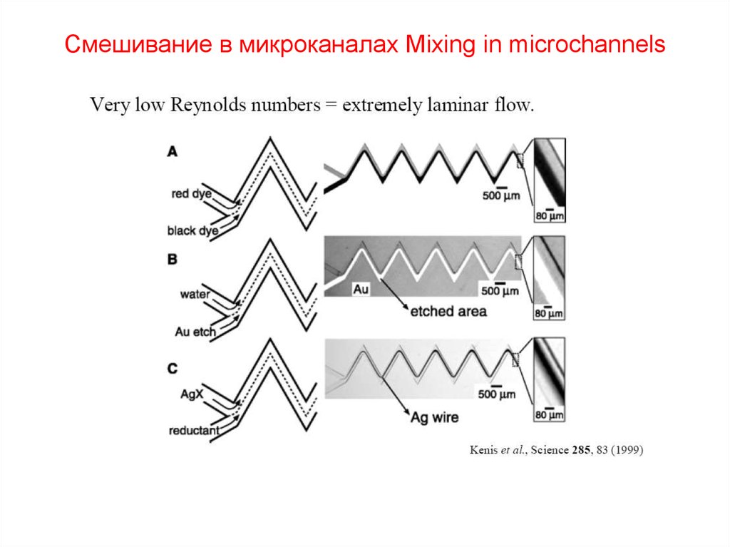
Смешивание в микроканалах Mixing in microchannels22. Смешивание в микроканалах Mixing in microchannels
Анализ ДНК - Lab on a Chip DNA analysis3’CAGTACGTCCAGCTGAGAC5’...
Bar code
Schematic of the microfluidic device. The device incorporates
a two-dimensional, hydrodynamic flow focusing design for stretching
individual l-phage DNA molecules. The sample is inserted into the
DNA port (left side) along with 1X TE buffer into each of the sheath
flow ports (top, bottom). Sample flow is from left to right. Inset: image
of the laser spot positioned in the backlit microfluidic channel. The
microfluidic channel is 5 mm wide in the interrogation region
highlighted by the alignment fiducials on either side of the channel.
Bar represents 25 mm. (Krogmeier, 2007)
23. Анализ ДНК - Lab on a Chip DNA analysis
Синтез ДНК DNA synthesisTwisted double-helix structure of DNA
Polymerase chain reaction (PCR).
Denaturing of the starting DNA template at
95ºC yields two strands, each containing all
of the necessary information to form a
complementary replica. The addition of
primers defines the starting point for
replication. At 60ºC, the DNA polymerase
enzyme catalyzes the reconstruction of the
complementary DNA strand from an ample
supply of nucleotides (dNTPs). The
reconstruction always proceeds in the 5’→3’
direction. The cycle ends with copies of two
portions of the helices, in addition to the
starting template. The cycle is then repeated.
The exploded view of three nucleotides
(CTG) in the denatured template shows their
chemical composition, including the 3’hydroxyl and 5’-phosphate groups.
24. Анализ ДНК
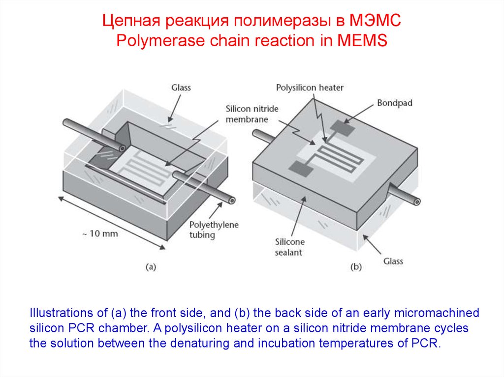
Цепная реакция полимеразы в МЭМСPolymerase chain reaction in MEMS
Illustrations of (a) the front side, and (b) the back side of an early micromachined
silicon PCR chamber. A polysilicon heater on a silicon nitride membrane cycles
the solution between the denaturing and incubation temperatures of PCR.
25. Синтез ДНК DNA synthesis
Электрофорезная сортировка ДНКElectrophoresis system for DNA separation
Illustration of the fluid injection and separation steps in a miniature DNA electrophoresis
system. An applied electric field electrophoretically pumps the fluid molecules from port
3 to port 1 during the injection step. Another applied voltage between ports 2 and 4
initiates the electrophoretic separation of the DNA molecules. The smearing of the fluid
plug in the separation channel is schematically illustrated. The capillary channels have
a typical cross section of 8 x 50 μm2. The separation capillary is 3.5 cm long.
26. Цепная реакция полимеразы в МЭМС Polymerase chain reaction in MEMS
Микроэлектроды Microelectrode arrayCross section of a microelectrode array showing two different metals for the
electrodes and for the bond pads. The schematic also illustrates a basic
electrical equivalent circuit that emphasizes the capacitive behavior of a
microelectrode. The silicon substrate and the silicon dioxide dielectric layer may
be substituted by an insulating glass substrate.
27. Электрофорезная сортировка ДНК Electrophoresis system for DNA separation
Анализ ДНК DNA analysisмассив
микроэлектродов
Illustration of the Nanogen electronic addressing and detection schemes. (a) A positive voltage attracts DNA
capture probes to biased microelectrodes. Negatively biased electrodes remain clear of DNA. Repetition of the
cycle in different solutions with appropriate electrode biasing sequentially builds an array of individually distinct
sites of DNA capture probes that differ by their sequence of nucleotides. (b) A DNA fragment with unknown
sequence hybridizes with a DNA capture probe with a complementary sequence. Fluorescence microscopy
reveals the hybridized site and, consequently, the unknown sequence.
28. Микроэлектроды Microelectrode array
Синтез массивов ДНК DNA synthesisWith 25 nucleotides
in a sequence, there
are 425 (equal to
1015) different
combinations that
can be made with
this process.
However, with a final
chip size of 1.28
cm2, there is only
enough space for
about 320,000
squares with
different sequences.
29. Анализ ДНК DNA analysis
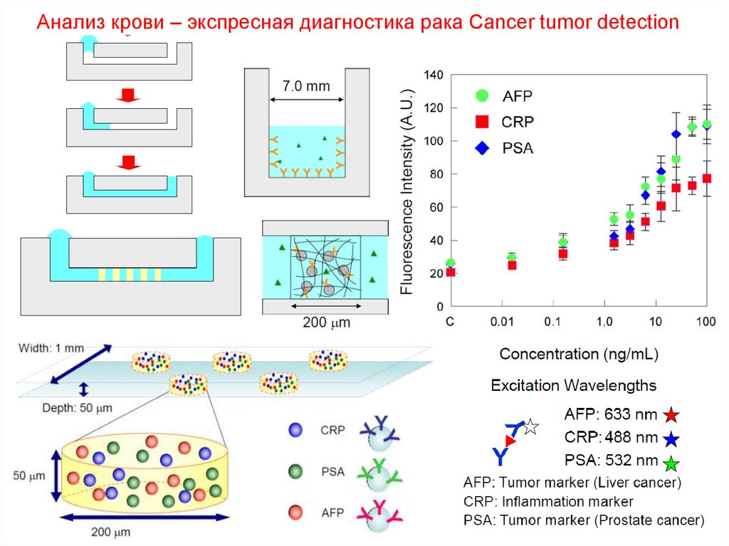
Анализ крови – экспресная диагностика рака Cancer tumor detection30. Синтез массивов ДНК DNA synthesis
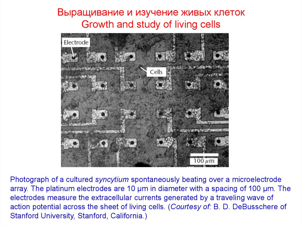
Выращивание и изучение живых клетокGrowth and study of living cells
Photograph of a cultured syncytium spontaneously beating over a microelectrode
array. The platinum electrodes are 10 μm in diameter with a spacing of 100 μm. The
electrodes measure the extracellular currents generated by a traveling wave of
action potential across the sheet of living cells. (Courtesy of: B. D. DeBusschere of
Stanford University, Stanford, California.)
31. Анализ крови – экспресная диагностика рака Cancer tumor detection
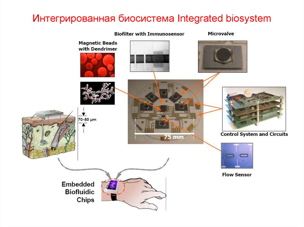
Интегрированная биосистема Integrated biosystem32. Выращивание и изучение живых клеток Growth and study of living cells
Заключение ConclusionМЭМС и НЭМС представляют собой обширное
семейство портативных приборов, датчиков и
устройств. Wide variety of portable devices.
World smallest car
Основным материалом НЭМС является кремний.
Material of choice for MEMS is Si.
Технологии НЭМС разработаны на базе
технологий полупроводниковой электроники.
MEMS technology is taken from electronics
World smallest guitar
Уровень технологии НЭМС обеспечивает
массовое производство надежных приборов и
устройств различного назначения. NEMS
technology allows mass production.
Основными областями применения НЭМС
являются биология и медицина, системы
безопасности, системы связи и навигации,
электроника и фотоника. Major application areas
are biology, medicine, safety systems, navigation,
communications, electronics, photonics
НЭМС представляют собой значимый и
быстрорастущий сектор современной экономики.
NEMS market is big and fast growing.
Virtual reality
system











 Физика


