Похожие презентации:
Seminar on kesterites
1. Seminar on Kesterites
Ma terials Sci ence & Technolog ySeminar on Kesterites
Carolin Fella
Laboratory for Thin Films and Photovoltaics
Empa, Swiss Federal Laboratories for Materials Science and Technology
Überlandstr. 129, 8600 Dübendorf, Switzerland
2. Outline
MotivationBasic properties
Crystal structure and phases
Defects/Doping
Solar cells
Limiting factors
Laboratory for Thin Films and Photovoltaics
Swiss Federal Laboratories for Materials Science and Technology
2
3. Motivation
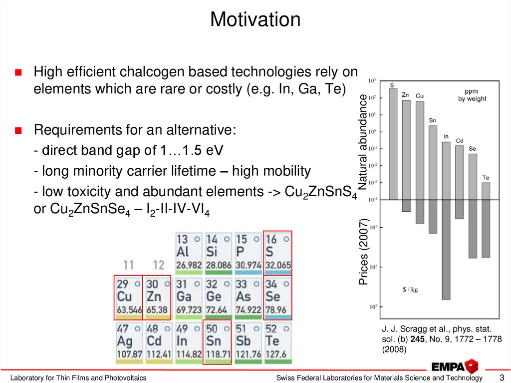
High efficient chalcogen based technologies rely onelements which are rare or costly (e.g. In, Ga, Te)
Requirements for an alternative:
- direct band gap of 1…1.5 eV
- long minority carrier lifetime – high mobility
- low toxicity and abundant elements -> Cu2ZnSnS4
or Cu2ZnSnSe4 – I2-II-IV-VI4
Prices (2007)
Natural abundance
J. J. Scragg et al., phys. stat.
sol. (b) 245, No. 9, 1772 – 1778
(2008)
Laboratory for Thin Films and Photovoltaics
Swiss Federal Laboratories for Materials Science and Technology
3
4. Material properties
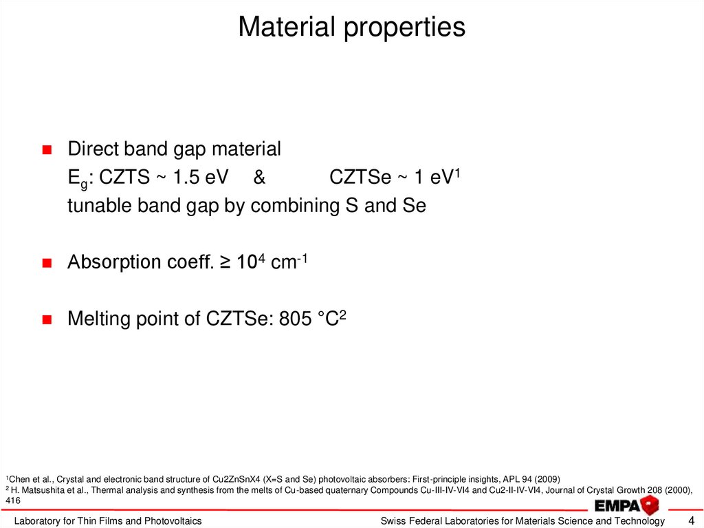
Direct band gap materialEg: CZTS ~ 1.5 eV &
CZTSe ~ 1 eV1
tunable band gap by combining S and Se
Absorption coeff. ≥ 104 cm-1
Melting point of CZTSe: 805 °C2
1Chen
2 H.
et al., Crystal and electronic band structure of Cu2ZnSnX4 (X=S and Se) photovoltaic absorbers: First-principle insights, APL 94 (2009)
Matsushita et al., Thermal analysis and synthesis from the melts of Cu-based quaternary Compounds Cu-III-IV-VI4 and Cu2-II-IV-VI4, Journal of Crystal Growth 208 (2000),
416
Laboratory for Thin Films and Photovoltaics
Swiss Federal Laboratories for Materials Science and Technology
4
5. Crystal structure
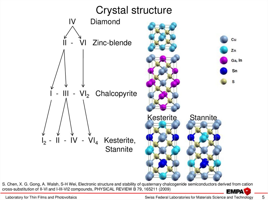
IVDiamond
II - VI Zinc-blende
, In
Sn
I - III - VI2 Chalcopyrite
Kesterite
Stannite
I2 - II - IV - VI4 Kesterite,
Stannite
S. Chen, X. G. Gong, A. Walsh, S-H Wei, Electronic structure and stability of quaternary chalcogenide semiconductors derived from cation
cross-substitution of II-VI and I-III-VI2 compounds, PHYSICAL REVIEW B 79, 165211 (2009)
Laboratory for Thin Films and Photovoltaics
Swiss Federal Laboratories for Materials Science and Technology
5
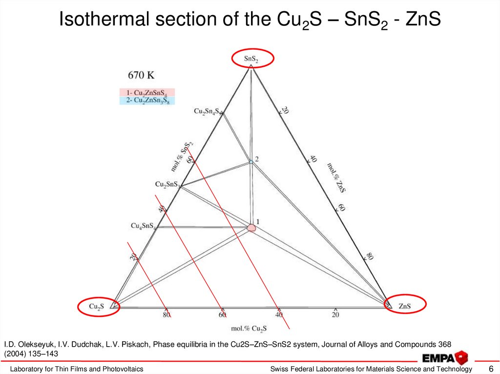
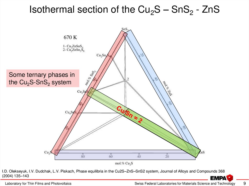
6. Isothermal section of the Cu2S – SnS2 - ZnS
I.D. Olekseyuk, I.V. Dudchak, L.V. Piskach, Phase equilibria in the Cu2S–ZnS–SnS2 system, Journal of Alloys and Compounds 368(2004) 135–143
Laboratory for Thin Films and Photovoltaics
Swiss Federal Laboratories for Materials Science and Technology
6
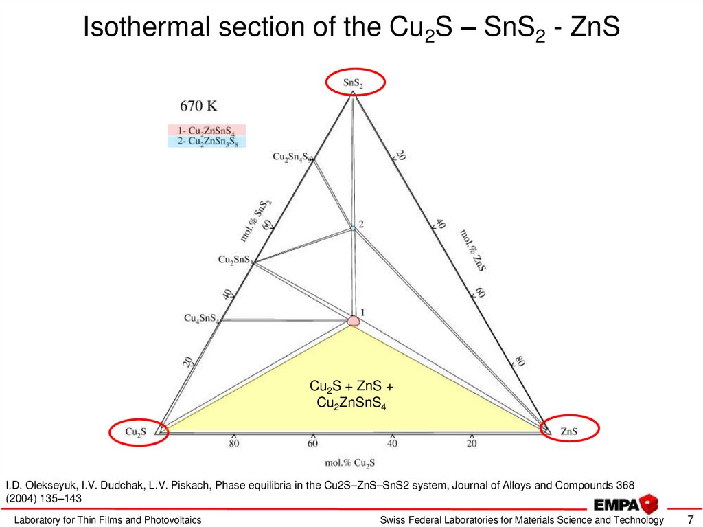
7. Isothermal section of the Cu2S – SnS2 - ZnS
Cu2S + ZnS +Cu2ZnSnS4
I.D. Olekseyuk, I.V. Dudchak, L.V. Piskach, Phase equilibria in the Cu2S–ZnS–SnS2 system, Journal of Alloys and Compounds 368
(2004) 135–143
Laboratory for Thin Films and Photovoltaics
Swiss Federal Laboratories for Materials Science and Technology
7
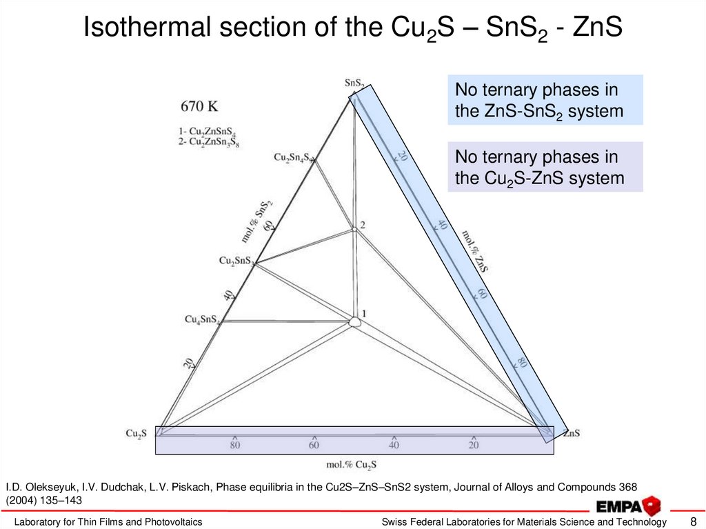
8. Isothermal section of the Cu2S – SnS2 - ZnS
No ternary phases inthe ZnS-SnS2 system
No ternary phases in
the Cu2S-ZnS system
I.D. Olekseyuk, I.V. Dudchak, L.V. Piskach, Phase equilibria in the Cu2S–ZnS–SnS2 system, Journal of Alloys and Compounds 368
(2004) 135–143
Laboratory for Thin Films and Photovoltaics
Swiss Federal Laboratories for Materials Science and Technology
8
9. Isothermal section of the Cu2S – SnS2 - ZnS
Some ternary phases inthe Cu2S-SnS2 system
I.D. Olekseyuk, I.V. Dudchak, L.V. Piskach, Phase equilibria in the Cu2S–ZnS–SnS2 system, Journal of Alloys and Compounds 368
(2004) 135–143
Laboratory for Thin Films and Photovoltaics
Swiss Federal Laboratories for Materials Science and Technology
9
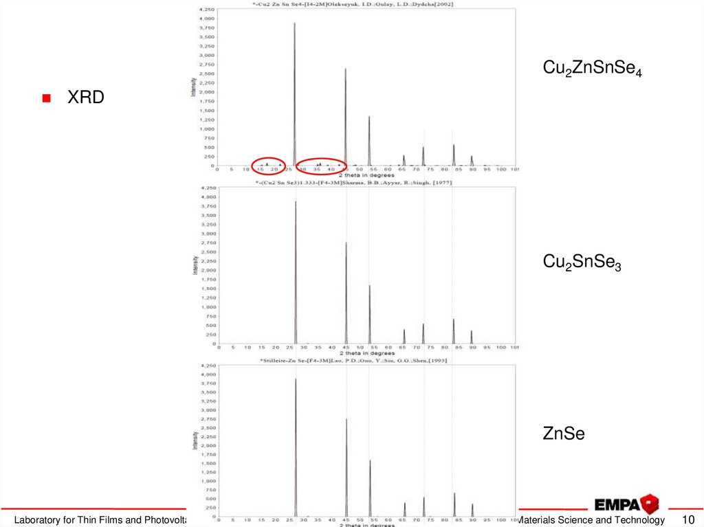
10. Kesterite characterization
Cu2ZnSnSe4XRD
Cu2SnSe3
ZnSe
Laboratory for Thin Films and Photovoltaics
Swiss Federal Laboratories for Materials Science and Technology
10
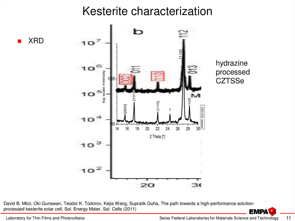
11. Kesterite characterization
XRDhydrazine
processed
CZTSSe
GI10D
103
[110]
[101]
1000
[002]
log scale Intensity
[112]
?
100
14
16
18
20
22
24
26
28
30
2 Theta [°]
David B. Mitzi, Oki Gunawan, Teodor K. Todorov, Kejia Wang, Supratik Guha, The path towards a high-performance solutionprocessed kesterite solar cell, Sol. Energy Mater. Sol. Cells (2011)
Laboratory for Thin Films and Photovoltaics
Swiss Federal Laboratories for Materials Science and Technology
11
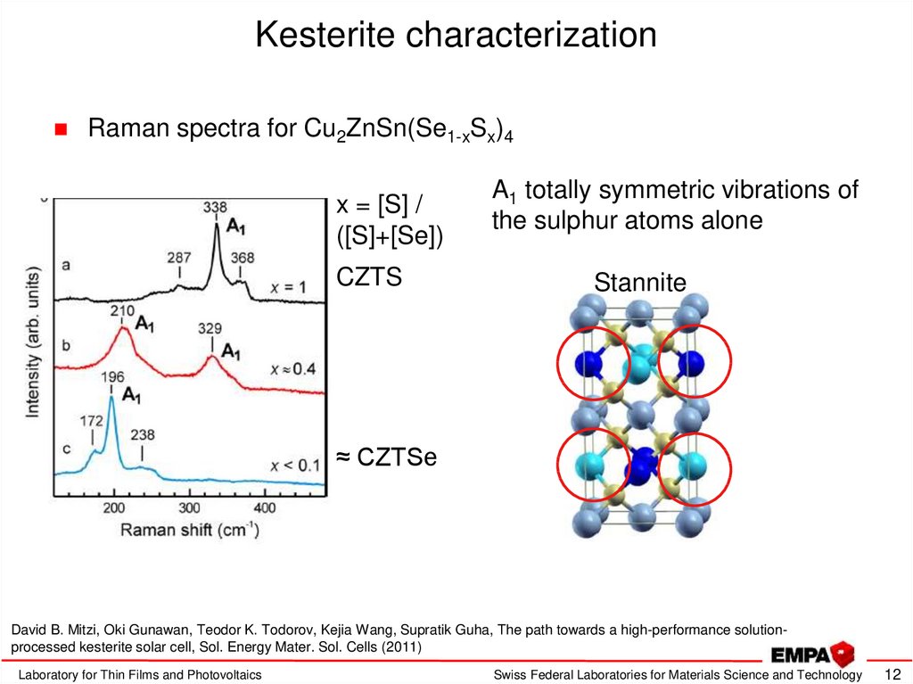
12. Kesterite characterization
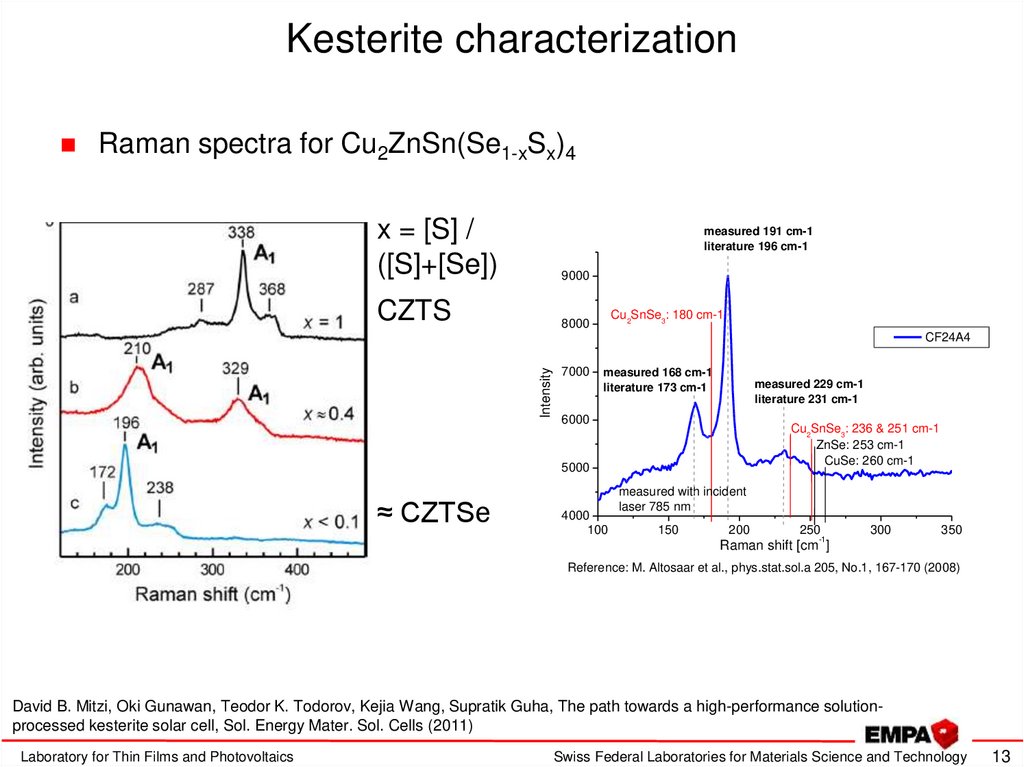
Raman spectra for Cu2ZnSn(Se1-xSx)4x = [S] /
([S]+[Se])
CZTS
A1 totally symmetric vibrations of
the sulphur atoms alone
Stannite
≈ CZTSe
David B. Mitzi, Oki Gunawan, Teodor K. Todorov, Kejia Wang, Supratik Guha, The path towards a high-performance solutionprocessed kesterite solar cell, Sol. Energy Mater. Sol. Cells (2011)
Laboratory for Thin Films and Photovoltaics
Swiss Federal Laboratories for Materials Science and Technology
12
13. Kesterite characterization
Raman spectra for Cu2ZnSn(Se1-xSx)4x = [S] /
([S]+[Se])
9000
CZTS
8000
measured 191 cm-1
literature 196 cm-1
Cu2SnSe3: 180 cm-1
Intensity
CF24A4
7000
measured 168 cm-1
literature 173 cm-1
measured 229 cm-1
literature 231 cm-1
6000
Cu2SnSe3: 236 & 251 cm-1
ZnSe: 253 cm-1
CuSe: 260 cm-1
5000
≈ CZTSe
4000
100
measured with incident
laser 785 nm
150
200
250
-1
300
350
Raman shift [cm ]
Reference: M. Altosaar et al., phys.stat.sol.a 205, No.1, 167-170 (2008)
David B. Mitzi, Oki Gunawan, Teodor K. Todorov, Kejia Wang, Supratik Guha, The path towards a high-performance solutionprocessed kesterite solar cell, Sol. Energy Mater. Sol. Cells (2011)
Laboratory for Thin Films and Photovoltaics
Swiss Federal Laboratories for Materials Science and Technology
13
14. Electrical properties
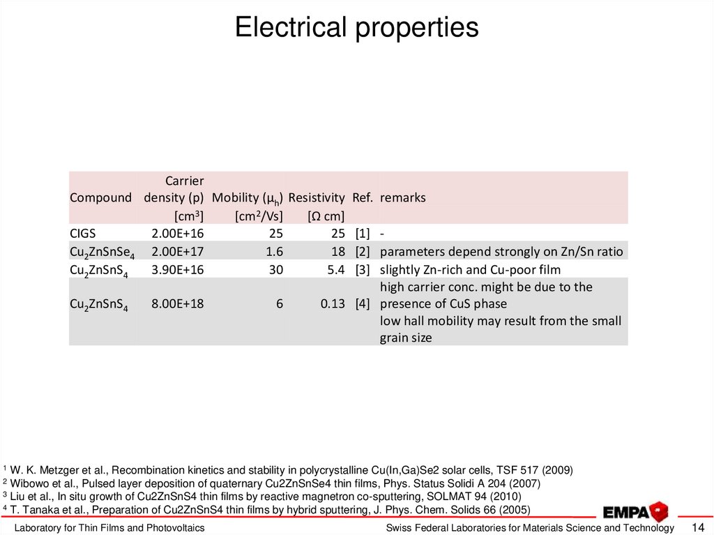
CarrierCompound density (p) Mobility (µh) Resistivity Ref. remarks
[cm3]
[cm2/Vs]
[Ω cm]
CIGS
2.00E+16
25
25 [1] Cu2ZnSnSe4 2.00E+17
1.6
18 [2] parameters depend strongly on Zn/Sn ratio
Cu2ZnSnS4
3.90E+16
30
5.4 [3] slightly Zn-rich and Cu-poor film
high carrier conc. might be due to the
Cu2ZnSnS4
8.00E+18
6
0.13 [4] presence of CuS phase
low hall mobility may result from the small
grain size
1
W. K. Metzger et al., Recombination kinetics and stability in polycrystalline Cu(In,Ga)Se2 solar cells, TSF 517 (2009)
Wibowo et al., Pulsed layer deposition of quaternary Cu2ZnSnSe4 thin films, Phys. Status Solidi A 204 (2007)
3 Liu et al., In situ growth of Cu2ZnSnS4 thin films by reactive magnetron co-sputtering, SOLMAT 94 (2010)
4 T. Tanaka et al., Preparation of Cu2ZnSnS4 thin films by hybrid sputtering, J. Phys. Chem. Solids 66 (2005)
2
Laboratory for Thin Films and Photovoltaics
Swiss Federal Laboratories for Materials Science and Technology
14
15. Intrinsic defects
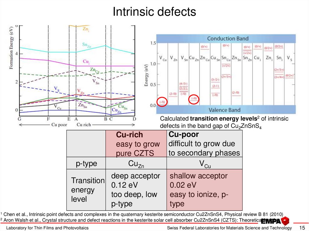
Calculated transition energy levels2 of intrinsicdefects in the band gap of Cu2ZnSnS4
Formation energy of neutral intrinsic defectsCu-rich
in CZTS
1
as a function of the chemical potential note, that the
formation energy will also depend on EF easy to grow
p-type
pure CZTS
CuZn
low formation energy of many
deep acceptor
Transition
acceptor defects will lead to0.12 eV
energy 1
intrinsic p-type character
too deep, low
level
1
2
p-type
Cu-poor
difficult to grow due
to secondary phases
VCu
shallow acceptor
0.02 eV
easy to ionize, ptype
Chen et al., Intrinsic point defects and complexes in the quaternary kesterite semiconductor Cu2ZnSnS4, Physical review B 81 (2010)
Aron Walsh et al., Crystal structure and defect reactions in the kesterite solar cell absorber Cu2ZnSnS4 (CZTS): Theoretical insights
Laboratory for Thin Films and Photovoltaics
Swiss Federal Laboratories for Materials Science and Technology
15
16. Defect complexes
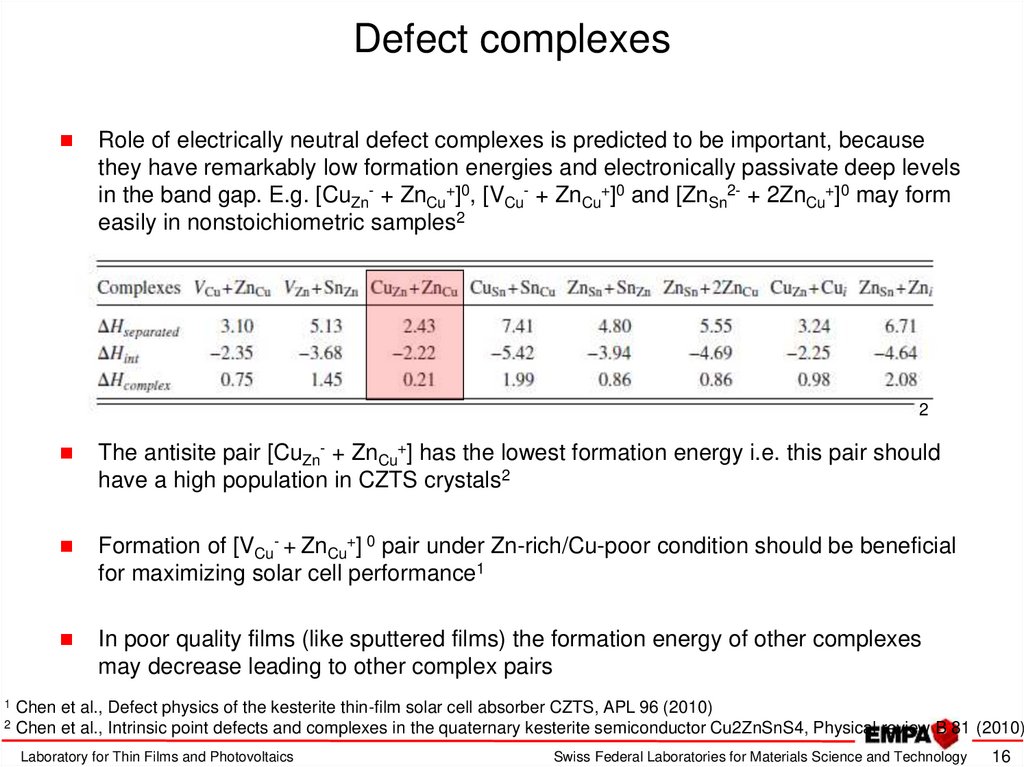
Role of electrically neutral defect complexes is predicted to be important, becausethey have remarkably low formation energies and electronically passivate deep levels
in the band gap. E.g. [CuZn- + ZnCu+]0, [VCu- + ZnCu+]0 and [ZnSn2- + 2ZnCu+]0 may form
easily in nonstoichiometric samples2
2
1
2
The antisite pair [CuZn- + ZnCu+] has the lowest formation energy i.e. this pair should
have a high population in CZTS crystals2
Formation of [VCu- + ZnCu+] 0 pair under Zn-rich/Cu-poor condition should be beneficial
for maximizing solar cell performance1
In poor quality films (like sputtered films) the formation energy of other complexes
may decrease leading to other complex pairs
Chen et al., Defect physics of the kesterite thin-film solar cell absorber CZTS, APL 96 (2010)
Chen et al., Intrinsic point defects and complexes in the quaternary kesterite semiconductor Cu2ZnSnS4, Physical review B 81 (2010)
Laboratory for Thin Films and Photovoltaics
Swiss Federal Laboratories for Materials Science and Technology
16
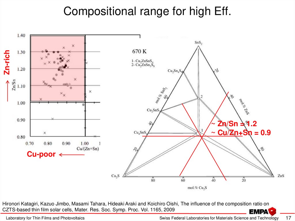
17. Compositional range for high Eff.
Zn-richCompositional range for high Eff.
~ Zn/Sn = 1.2
~ Cu/Zn+Sn = 0.9
Cu-poor
Hironori Katagiri, Kazuo Jimbo, Masami Tahara, Hideaki Araki and Koichiro Oishi, The influence of the composition ratio on
CZTS-based thin film solar cells, Mater. Res. Soc. Symp. Proc. Vol. 1165, 2009
Laboratory for Thin Films and Photovoltaics
Swiss Federal Laboratories for Materials Science and Technology
17
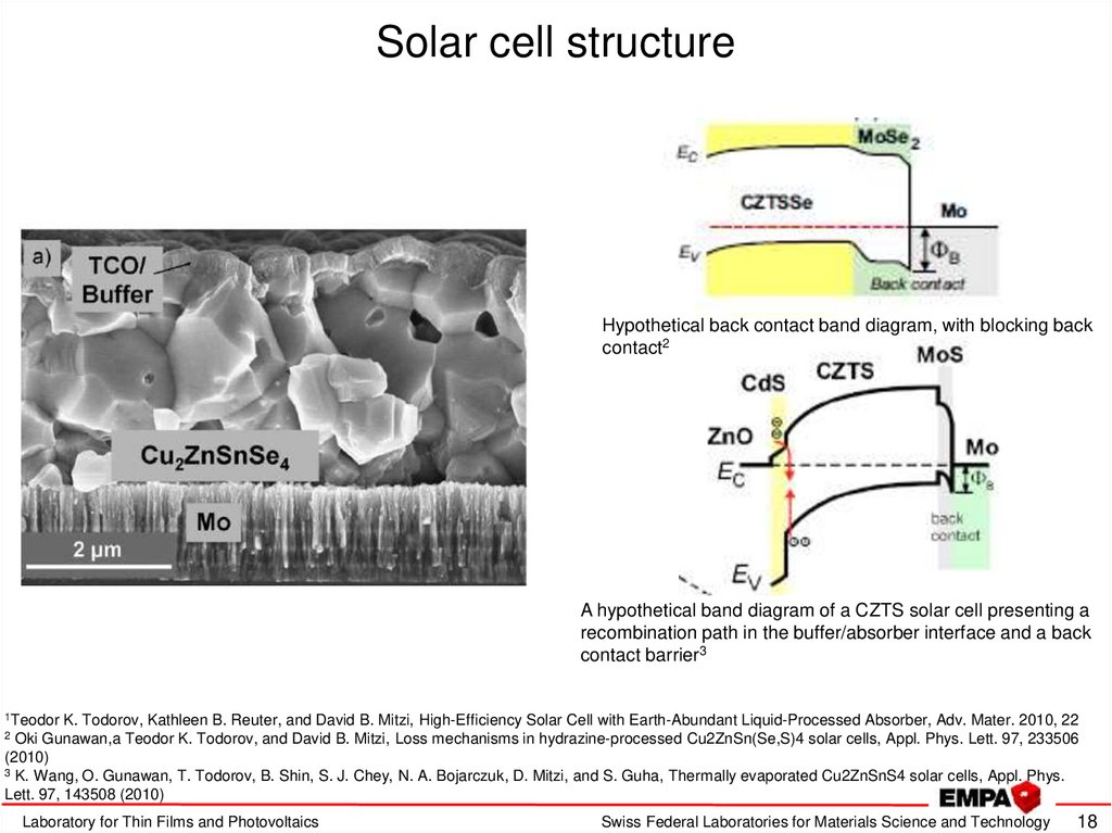
18. Solar cell structure
Hypothetical back contact band diagram, with blocking backcontact2
A hypothetical band diagram of a CZTS solar cell presenting a
recombination path in the buffer/absorber interface and a back
contact barrier3
1Teodor
K. Todorov, Kathleen B. Reuter, and David B. Mitzi, High-Efficiency Solar Cell with Earth-Abundant Liquid-Processed Absorber, Adv. Mater. 2010, 22
Oki Gunawan,a Teodor K. Todorov, and David B. Mitzi, Loss mechanisms in hydrazine-processed Cu2ZnSn(Se,S)4 solar cells, Appl. Phys. Lett. 97, 233506
(2010)
3 K. Wang, O. Gunawan, T. Todorov, B. Shin, S. J. Chey, N. A. Bojarczuk, D. Mitzi, and S. Guha, Thermally evaporated Cu2ZnSnS4 solar cells, Appl. Phys.
Lett. 97, 143508 (2010)
2
Laboratory for Thin Films and Photovoltaics
Swiss Federal Laboratories for Materials Science and Technology
18
19. Deposition methods
Vacuumsputteringbased
CZTS: 6.77 % (Katagiri) –
stacked metal sulfides
Mo/Cu/SnS2/ZnS (5 times)
CZTSe: 3.2 % (Zoppi) –
stacked metals Mo/Cu/Zn/Sn
evaporationbased
CZTS: 6.8 % (Wang, IBM)
co-evaporation from Cu, Zn, Sn,
S sources
Laboratory for Thin Films and Photovoltaics
Non-vacuum
electrodeposition
CZTS: 3.4 % (Ennaoui) –
co-electrodeposition
Ink-based
CZTSSe: 9.7 % (Todorov) –
dissolved (CuS, SnS2) and
Solid (ZnS) chalcogenides in
hydrazine
nanoparticles
CZTSSe: 7.2 % (Guo) –
selenization of CZTS nanocrystals
deposited by knife coating
Swiss Federal Laboratories for Materials Science and Technology
19
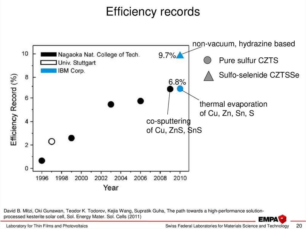
20. Efficiency records
non-vacuum, hydrazine based9.7%
Pure sulfur CZTS
Sulfo-selenide CZTSSe
6.8%
thermal evaporation
of Cu, Zn, Sn, S
co-sputtering
of Cu, ZnS, SnS
David B. Mitzi, Oki Gunawan, Teodor K. Todorov, Kejia Wang, Supratik Guha, The path towards a high-performance solutionprocessed kesterite solar cell, Sol. Energy Mater. Sol. Cells (2011)
Laboratory for Thin Films and Photovoltaics
Swiss Federal Laboratories for Materials Science and Technology
20
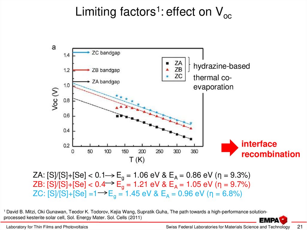
21. Limiting factors1: effect on Voc
hydrazine-basedthermal coevaporation
interface
recombination
ZA: [S]/[S]+[Se] < 0.1 Eg = 1.06 eV & EA = 0.86 eV (η = 9.3%)
ZB: [S]/[S]+[Se] < 0.4 Eg = 1.21 eV & EA = 1.05 eV (η = 9.7%)
ZC: [S]/[S]+[Se] =1 Eg = 1.45 eV & EA = 0.96 eV (η = 6.8%)
1 David
B. Mitzi, Oki Gunawan, Teodor K. Todorov, Kejia Wang, Supratik Guha, The path towards a high-performance solutionprocessed kesterite solar cell, Sol. Energy Mater. Sol. Cells (2011)
Laboratory for Thin Films and Photovoltaics
Swiss Federal Laboratories for Materials Science and Technology
21
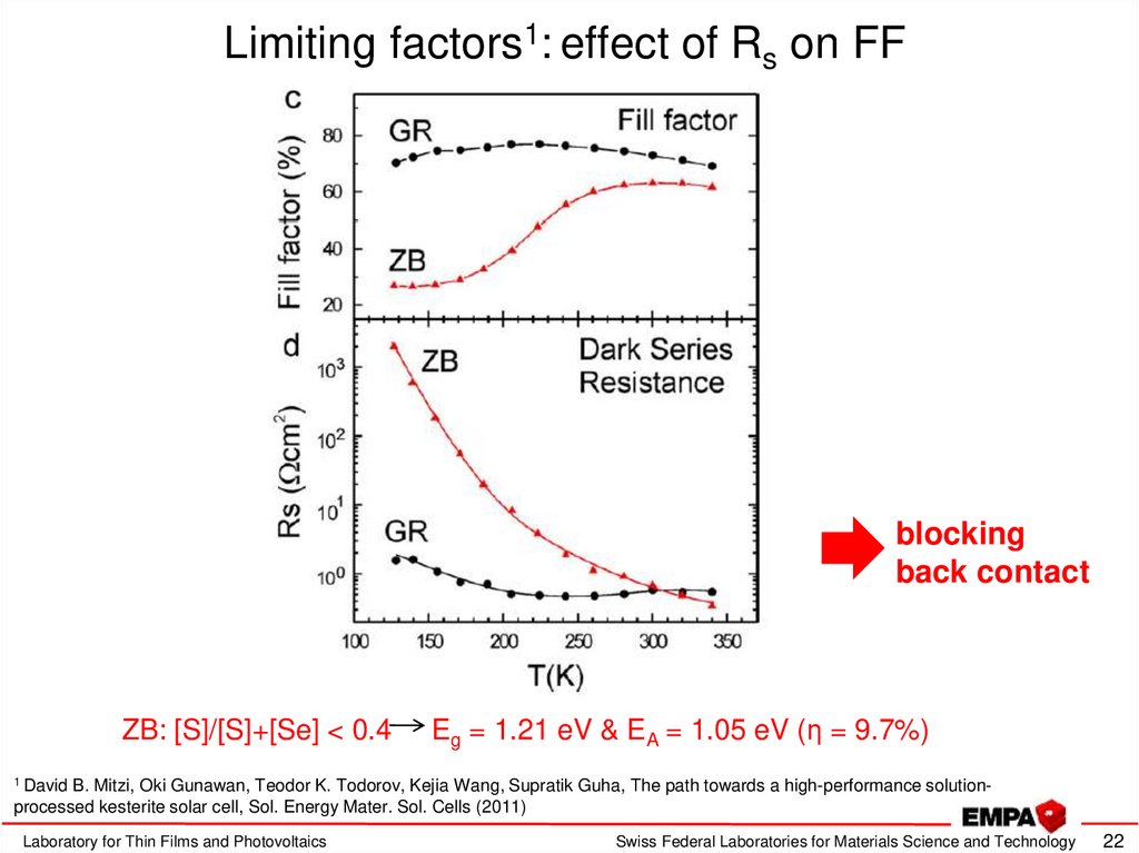
22. Limiting factors1: effect of Rs on FF
blockingback contact
ZB: [S]/[S]+[Se] < 0.4
Eg = 1.21 eV & EA = 1.05 eV (η = 9.7%)
1 David
B. Mitzi, Oki Gunawan, Teodor K. Todorov, Kejia Wang, Supratik Guha, The path towards a high-performance solutionprocessed kesterite solar cell, Sol. Energy Mater. Sol. Cells (2011)
Laboratory for Thin Films and Photovoltaics
Swiss Federal Laboratories for Materials Science and Technology
22
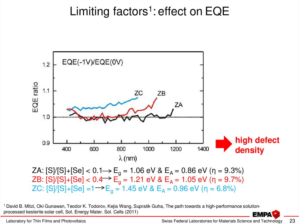
23. Limiting factors1: effect on EQE
high defectdensity
ZA: [S]/[S]+[Se] < 0.1 Eg = 1.06 eV & EA = 0.86 eV (η = 9.3%)
ZB: [S]/[S]+[Se] < 0.4 Eg = 1.21 eV & EA = 1.05 eV (η = 9.7%)
ZC: [S]/[S]+[Se] =1 Eg = 1.45 eV & EA = 0.96 eV (η = 6.8%)
1 David
B. Mitzi, Oki Gunawan, Teodor K. Todorov, Kejia Wang, Supratik Guha, The path towards a high-performance solutionprocessed kesterite solar cell, Sol. Energy Mater. Sol. Cells (2011)
Laboratory for Thin Films and Photovoltaics
Swiss Federal Laboratories for Materials Science and Technology
23
24. Conclusions
Formation and identification of parasitic phases (Cu2SnS3,Cu4SnS4, ZnS)
Metal ratio control: Cu-poor / Zn-rich important to control nature of
electrical defects (CuZn, VCu and defect complexes)
Conventional Mo/CZTSSe/CdS/ZnO structure: 6.8% (by
evaporation/ co-sputtering), 9.7% (based on hydrazine solutions)
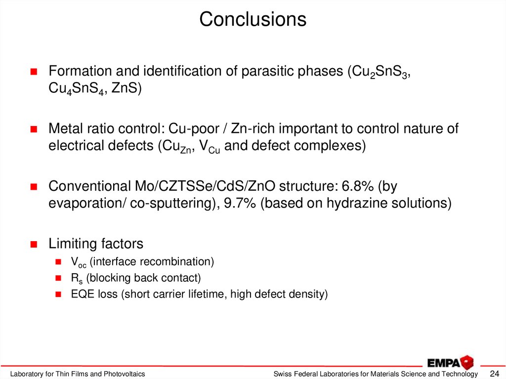
Limiting factors
Voc (interface recombination)
Rs (blocking back contact)
EQE loss (short carrier lifetime, high defect density)
Laboratory for Thin Films and Photovoltaics
Swiss Federal Laboratories for Materials Science and Technology
24
25. Folie 25
Thank you for your attention !Laboratory for Thin Films and Photovoltaics
Swiss Federal Laboratories for Materials Science and Technology
25
26. Folie 26
Back up sildesLaboratory for Thin Films and Photovoltaics
Swiss Federal Laboratories for Materials Science and Technology
26
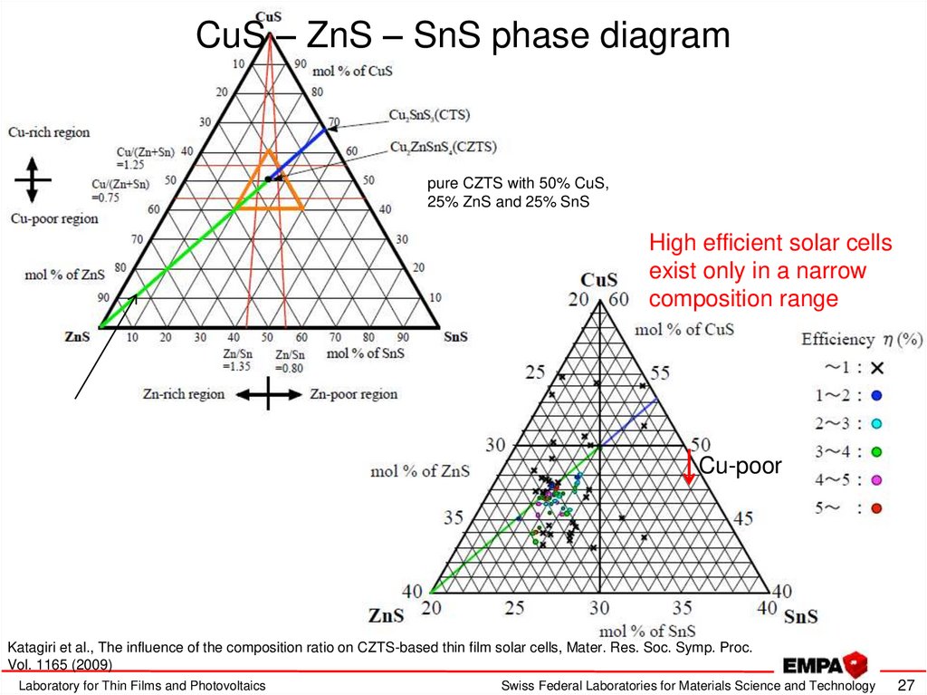
27. CuS – ZnS – SnS phase diagram
pure CZTS with 50% CuS,25% ZnS and 25% SnS
High efficient solar cells
exist only in a narrow
composition range
Cu-poor
Katagiri et al., The influence of the composition ratio on CZTS-based thin film solar cells, Mater. Res. Soc. Symp. Proc.
Vol. 1165 (2009)
Laboratory for Thin Films and Photovoltaics
Swiss Federal Laboratories for Materials Science and Technology
27
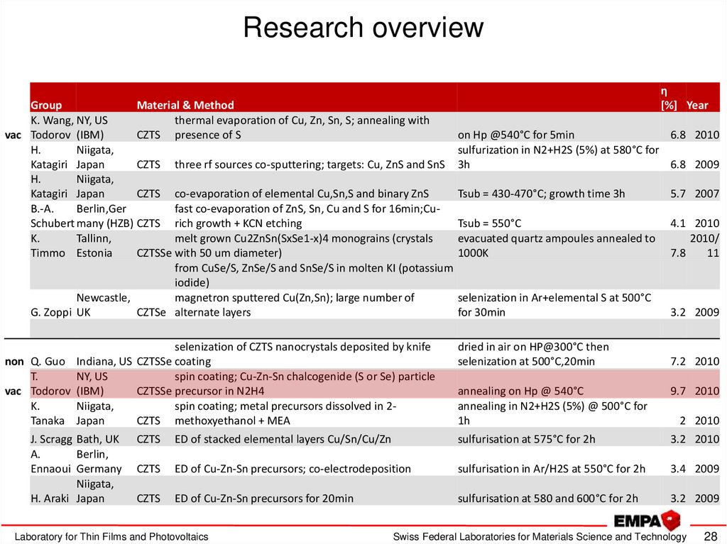
28. Research overview
GroupMaterial & Method
K. Wang, NY, US
thermal evaporation of Cu, Zn, Sn, S; annealing with
vac Todorov (IBM)
CZTS presence of S
H.
Niigata,
Katagiri Japan
CZTS three rf sources co-sputtering; targets: Cu, ZnS and SnS
H.
Niigata,
Katagiri Japan
CZTS co-evaporation of elemental Cu,Sn,S and binary ZnS
B.-A.
Berlin,Ger
fast co-evaporation of ZnS, Sn, Cu and S for 16min;CuSchubert many (HZB) CZTS rich growth + KCN etching
K.
Tallinn,
melt grown Cu2ZnSn(SxSe1-x)4 monograins (crystals
Timmo Estonia
CZTSSe with 50 um diameter)
from CuSe/S, ZnSe/S and SnSe/S in molten KI (potassium
iodide)
Newcastle,
magnetron sputtered Cu(Zn,Sn); large number of
G. Zoppi UK
CZTSe alternate layers
selenization of CZTS nanocrystals deposited by knife
non Q. Guo Indiana, US CZTSSe coating
T.
NY, US
spin coating; Cu-Zn-Sn chalcogenide (S or Se) particle
vac Todorov (IBM)
CZTSSe precursor in N2H4
K.
Niigata,
spin coating; metal precursors dissolved in 2Tanaka Japan
CZTS methoxyethanol + MEA
J. Scragg Bath, UK
A.
Berlin,
Ennaoui Germany
Niigata,
H. Araki Japan
η
[%] Year
on Hp @540°C for 5min
6.8 2010
sulfurization in N2+H2S (5%) at 580°C for
3h
6.8 2009
Tsub = 430-470°C; growth time 3h
5.7 2007
Tsub = 550°C
evacuated quartz ampoules annealed to
1000K
4.1 2010
2010/
7.8
11
selenization in Ar+elemental S at 500°C
for 30min
3.2 2009
dried in air on HP@300°C then
selenization at 500°C,20min
7.2 2010
annealing on Hp @ 540°C
annealing in N2+H2S (5%) @ 500°C for
1h
9.7 2010
2 2010
CZTS
ED of stacked elemental layers Cu/Sn/Cu/Zn
sulfurisation at 575°C for 2h
3.2 2010
CZTS
ED of Cu-Zn-Sn precursors; co-electrodeposition
sulfurisation in Ar/H2S at 550°C for 2h
3.4 2009
CZTS
ED of Cu-Zn-Sn precursors for 20min
sulfurisation at 580 and 600°C for 2h
3.2 2009
Laboratory for Thin Films and Photovoltaics
Swiss Federal Laboratories for Materials Science and Technology
28
29. Phase diagram of Cu2S – SnS2
α high temp Cu2S phaseα' medium temp Cu2S phase
γ SnS2 phase
α'' low temp Cu2S phase
I.D. Olekseyuk, I.V. Dudchak, L.V. Piskach, Phase equilibria in the Cu2S–ZnS–SnS2 system, Journal of Alloys and Compounds 368
(2004) 135–143
Laboratory for Thin Films and Photovoltaics
Swiss Federal Laboratories for Materials Science and Technology
29
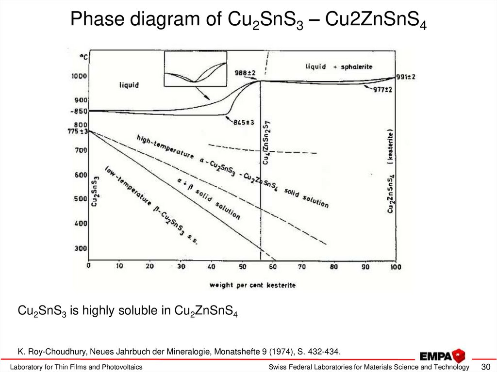
30. Phase diagram of Cu2SnS3 – Cu2ZnSnS4
Cu2SnS3 is highly soluble in Cu2ZnSnS4K. Roy-Choudhury, Neues Jahrbuch der Mineralogie, Monatshefte 9 (1974), S. 432-434.
Laboratory for Thin Films and Photovoltaics
Swiss Federal Laboratories for Materials Science and Technology
30
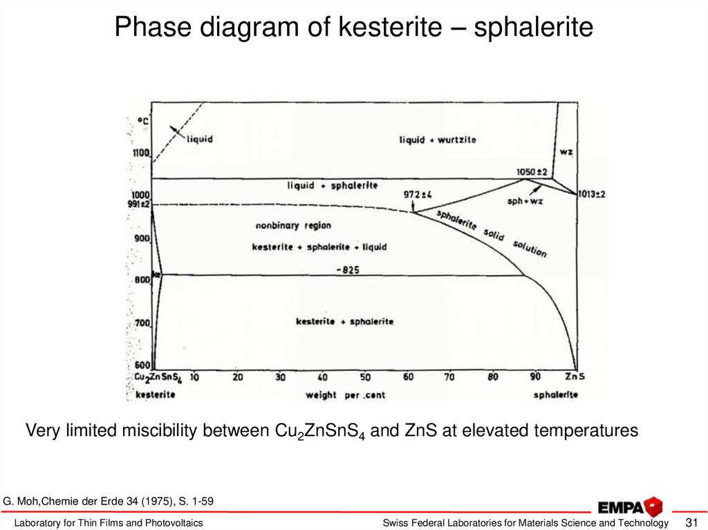
31. Phase diagram of kesterite – sphalerite
Very limited miscibility between Cu2ZnSnS4 and ZnS at elevated temperaturesG. Moh,Chemie der Erde 34 (1975), S. 1-59
Laboratory for Thin Films and Photovoltaics
Swiss Federal Laboratories for Materials Science and Technology
31
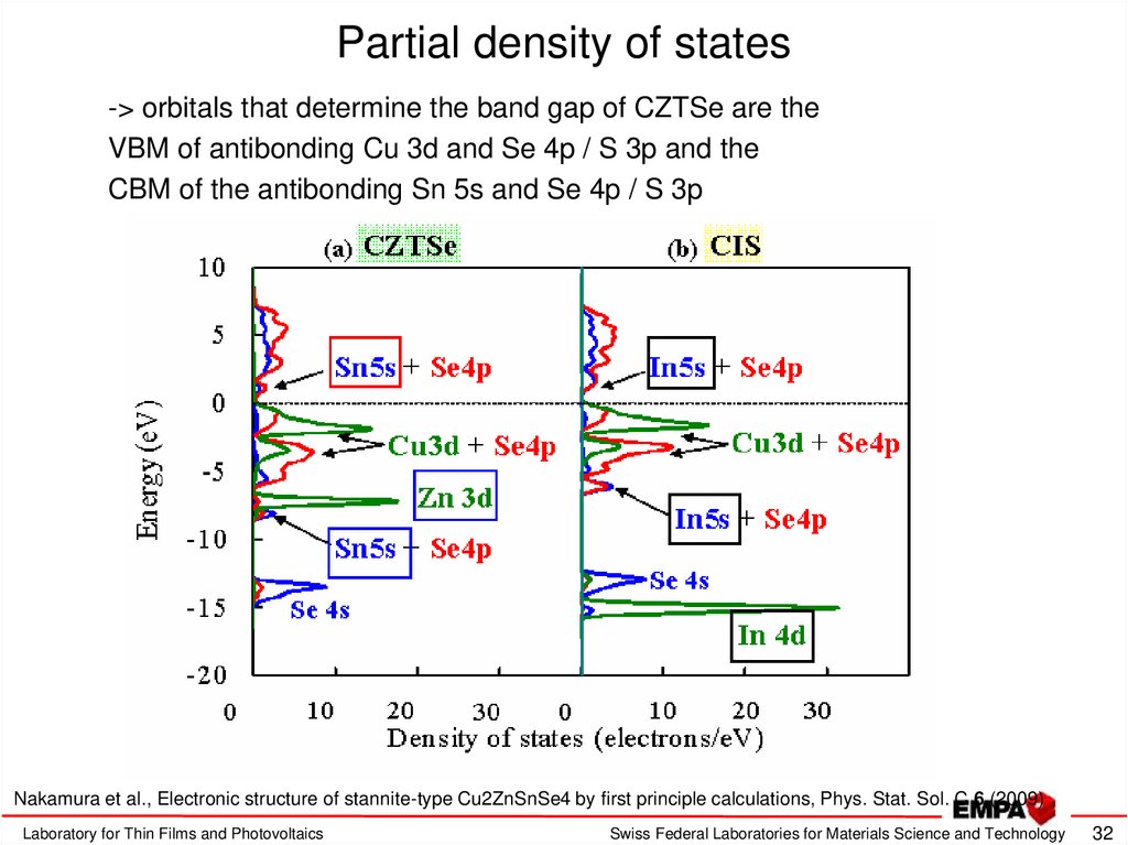
32. Partial density of states
-> orbitals that determine the band gap of CZTSe are theVBM of antibonding Cu 3d and Se 4p / S 3p and the
CBM of the antibonding Sn 5s and Se 4p / S 3p
Nakamura et al., Electronic structure of stannite-type Cu2ZnSnSe4 by first principle calculations, Phys. Stat. Sol. C 6 (2009)
Laboratory for Thin Films and Photovoltaics
Swiss Federal Laboratories for Materials Science and Technology
32
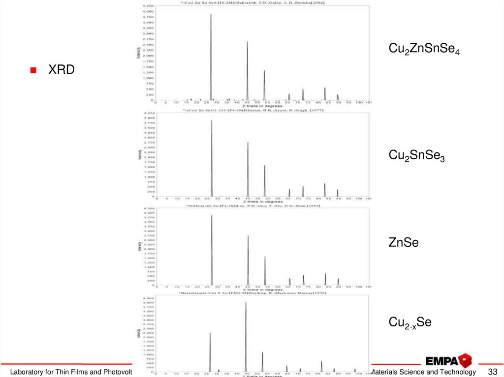
33. Kesterite characterization
Cu2ZnSnSe4XRD
Cu2SnSe3
ZnSe
Cu2-xSe
Laboratory for Thin Films and Photovoltaics
Swiss Federal Laboratories for Materials Science and Technology
33


 Химия
Химия


