 product feature analysis")


 PCB Stack up")
 PCB Stack up")


 Электроника
Похожие презентации:


")
")

")


System Architecture block diagram
1. NBG1 Training Course FM8(Hanks) product feature analysis
By: JonySeptember,2008
2. Agenda
System Architecture block diagramPCBA Outline drawing
System major components
Key feature for key chip
Power sequence diagram
Power check and power on troubleshooting
Q&A
3. System Architecture block diagram
4. System Architecture block diagram
5. PCBA Outline drawing
6. PCBA Outline drawing
7. FM8 (DIS) PCB Stack up
8. FM8B (UMA) PCB Stack up
9. System major components
FunctionVender Part #
Package
Vender
CPU
Penryn
PGA
Intel
North bridge
Cantiga
BGA
Intel
South bridge
ICH9-M
BGA
Intel
Ultra I/O
ITE8512E
LQFP
ITE
Keyboard controller
ITE8512E
LQFP
ITE
Graphics
ATI –M92-XT
BGA
ATI
10. System major components
FunctionVender part#
Package
Vender
Flash BIOS
SST25VF016B SOIC
SST
CardBus
R5C833
TQFP
RICOH
Express Card
ICH9-M
BGA
Intel
LAN Controller
BCM5784M
QFN
Broadcom
Clock
SLG8SP513V
QFN
Silego
Thermal
SMSC1423
MSOP
SMSC
11.
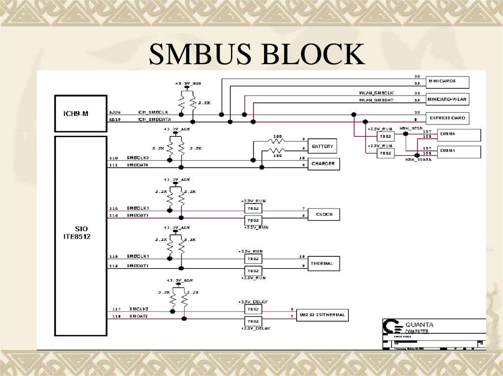
SMBUS BLOCK12. Key feature
CPU-Intel Penryn Dual Core Processor(1.6GHz-3.06GHz,45nm,1066MHZ,6M/3M L2)
uFC-PGA Package 478 pins 800/1066 MHZ FSB
VCORE Range:0.95V- 1.2V
VID Range:0V -1.5V.
◆BIOS 2M Flash ROM (SST SST25VF016B)
SPI interface
+3.3V_ALW support BIOS chip.
13. Key feature
North bridge-Intel Cantiga memory controllerHub.
Support 667/800MHZ DDRII, dual channel .
Support PCIE graphics (PCIE x16), which
support LVDS, HDMI(ATI), CRT interface.
Support DMI interface to the south bridge.
+1.05V_VCCP,+1.5V_RUN,+1.8V_SUS for
MCH Power plane
14. Key feature
South bridge-Intel ICH9-M I/O controller Hub.33MHZ PCI Bus for CardBus/1394 interface.
Support PCIE x1 Express-Card
Support PCIE x3 MINI-CARD(WLAN and WWAN and
WPAN)
Support PCIE x1 BCM5784M
Support USB x3 USB2.0 interface.
DMI( Direct Media interface)
SATA interface
LPC interface
SPI interface to ITE8512.
+1.5V_RUN,+1.05V_VCCP,+3.3V_SUS,+1.5V_SUS
support ICH9 Power plane
15. Key feature
SIO-ITE 8512K/B controller include in ITE 8512
SPI/LPC support
Power on/off management &GPIO support.
PS/2 to Touchpad
+3V_ALW support SIO power plane
16. Key feature
LOM-Broadcom5784MSupport 10/100/1000M
Support MINI antenna for WLAN
Support WWAN
VCORE=3.3V_LAN,1.2V_LAN,2.5V_LAN.
17. Key feature
Graphics: Intel GM45 Integrated graphicscontroller & ATI M92 XT(For discrete
FM8,FM8B UMA internal graphics)
Gfx Chip on board (For PM45)
Video Memory 512MB 800MHz
+VCC_GFX_CORE=0.9V,1.0V,1.1V and 1.2V
& +1.1V_GFX_PCIE support M92 XT power
plane
18. Power Hierarchy
Level 4: RUNLevel 2: ALW
+3.3V_RUN,+5V_RUN,+1.8V_
RUN,+1.5V_RUN,VCC_Core.
+3.3V_SUS,+5V_SUS,1.8V_S
US,+1.5V_SUS (UMA)
+3.3V_ALW,+5V_ALW,15V
Level 1: RTC _PWR
+3.3V_RTC_LDO,+RTC_Cell
Level 0: Power Source
+DC_IN, Power Source
Level 3: SUS
19. Power sequence diagram
20. Power sequence
Please check the Wordfile in detail
21. Power check and power on troubleshooting
1. Power Check1
Check +PWR_SRC/DC_IN 19.5V=19.5V
Check +3.3V_ALW =3.3V
End
Check +DCIN_JACK
N
N
Check PC154 Pin1 and PU5
22. Power check and power on troubleshooting
Power On/ Staring checkPWR_SW#=Low pulse
Check +5V_ALW2=5V
Check SUS_ON=H
Check +3.3V_SUS
Check +5V_SUS
Check 1.8V_SUS
N
N
N
N
Check +3.3v_ALW
MAX17020ET
Check ITE8512 Pin100
FDC655BN
N
MAX17020ET
N
TPS51116PWPRG4
23. Power check and power on troubleshooting
Power on/staring checkCheck SLP_S3#
N
Check RUN_ON1
N
Check RUN_ON
N
1.Check +5V_RUN
2.Check +3V_RUN
3.Check +1.5V_RUN
4.Check +1.5V_SUS(UMA)
5.Check +1.8V_RUN
N
Check +VCC_GFX_CORE
N
Check HWPG
N
Check ICH9 SLP_S3# Pin
Check ITE8512 Pin123
Check U10 Pin4
1.PQ10 - SI4800BDY-T1-E3
2.PQ14 - FDS8880_NL
3.Check PU6 and PC95
4.Check U35 Pin5
5.Check PQ7 Pin1,2,3
Check MAX8632ETI+
Check - SN74AHC08PW Pin11
24. Power check and power on troubleshooting
Power on/staring checkCheck IMVP_VR_ON
Check VCC_CORE
Check PCI_RST#
CPU_RST#
End
N
N
Check ITE8512 Pin95 and ISL6262ACRZ-T Pin44
Check ISL6262ACRZ-T
N
Check TC7SZ32FU Pin4
N
Check MCH B6
25. Q&A
Q&AThanks Everyone