


 Электроника
Похожие презентации:


")


P9X79 Series Confidential
1.
2012 EU ALSA TrainingP9X79 SERIES
Confidential
2.
P9X79 – AgendaIntel X79 Platform Structure
P9X79 Series Architecture
New Feature
Difference With P8 Series
Clock Distribution
Power Flow & Critical Power on X79 Platform
Power Sequence
Embedded Controller Introducing
SIO and Other Power Chipset Introducing
Communication BUS Introducing
3.
P9X79 – AgendaIntel X79 Platform Structure
P9X79 Series Architecture
New Feature
Difference With P8 Series
Clock Distribution
Power Flow & Critical Power on X79 Platform
Power Sequence
Embedded Controller Introducing
SIO and Other Power Chipset Introducing
Power theory and working condition
Communication BUS Introducing
4.
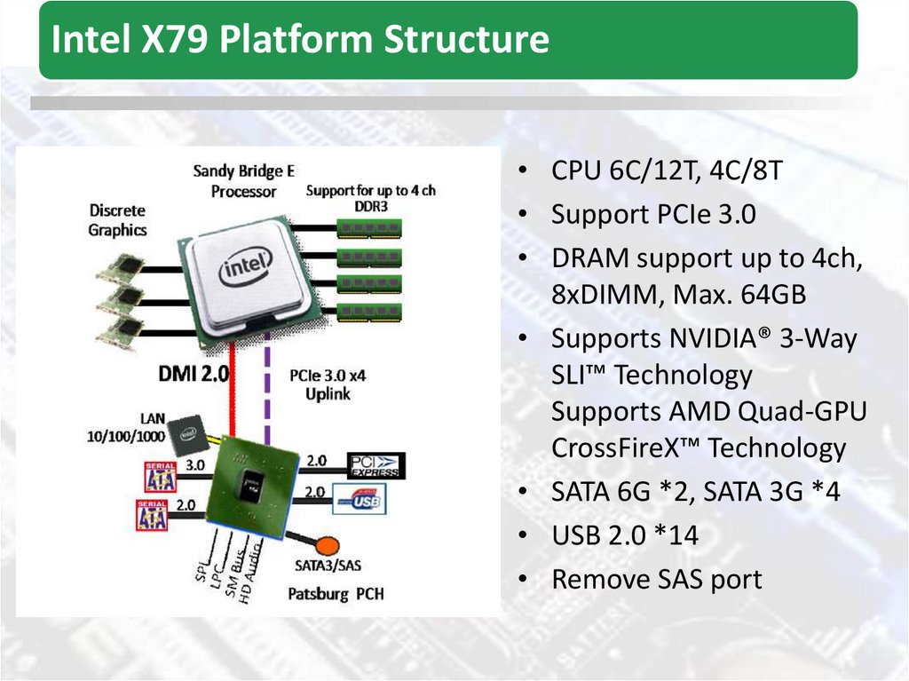
Intel X79 Platform Structure• CPU 6C/12T, 4C/8T
• Support PCIe 3.0
• DRAM support up to 4ch,
8xDIMM, Max. 64GB
• Supports NVIDIA® 3-Way
SLI™ Technology
Supports AMD Quad-GPU
CrossFireX™ Technology
• SATA 6G *2, SATA 3G *4
• USB 2.0 *14
• Remove SAS port
5.
Intel X79 Platform Structure• Support 8GB,MAX is for 64GB
• Support DDR3 2400(O.C.)/2133(O.C.)
1866/1600/1333/1066
• Support Intel® Extreme Memory
Profile(XMP)
• Support DIGI+ Power Control
• 2 + 2 Phase Control
6.
P9X79 – AgendaIntel X79 Platform Structure
P9X79 Series Architecture
New Feature
Difference With P8 Series
Clock Distribution
Power Flow & Critical Power on X79 Platform
Power Sequence
Embedded Controller Introducing
SIO and Other Power Chipset Introducing
Power theory and working condition
Communication BUS Introducing
7.
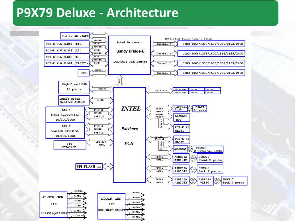
P9X79 Deluxe - ArchitectureP9X79 DELUXE
2011.12.12
Rev 1.03B
VRD 12 on Board
128-bit Dual-Channel Memory x 4 Slots
100MHz
PCI-E X16 SLOT1 (X16)
Intel Processor
PCI-E
Channel A
DDR3 1066/1333/1600/1866/2133/2400
Channel B
DDR3 1066/1333/1600/1866/2133/2400
Channel C
DDR3 1066/1333/1600/1866/2133/2400
Channel D
DDR3 1066/1333/1600/1866/2133/2400
100MHz
PCI-E X16 SLOT2 (X8)
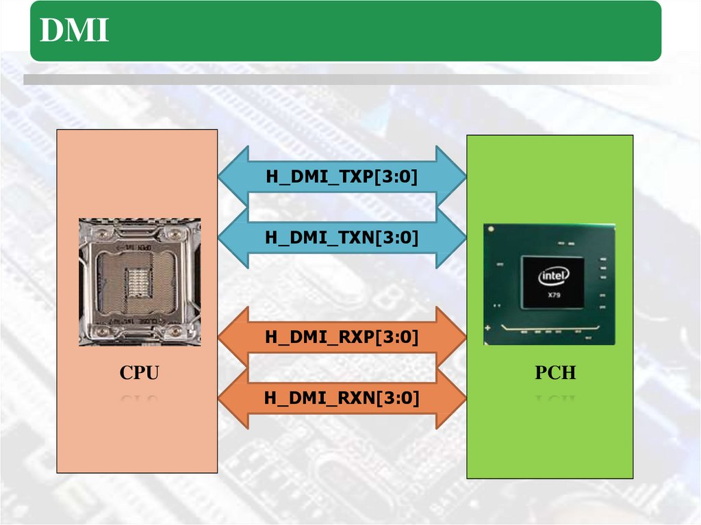
PCI-E
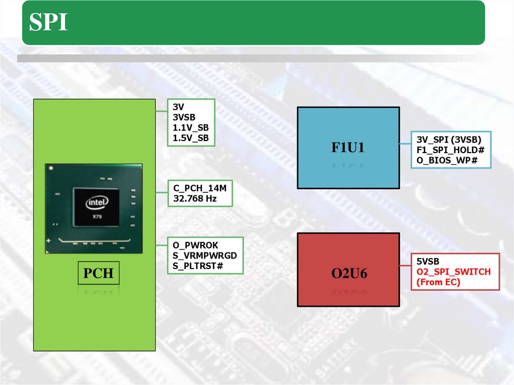
Sandy Bridge-E
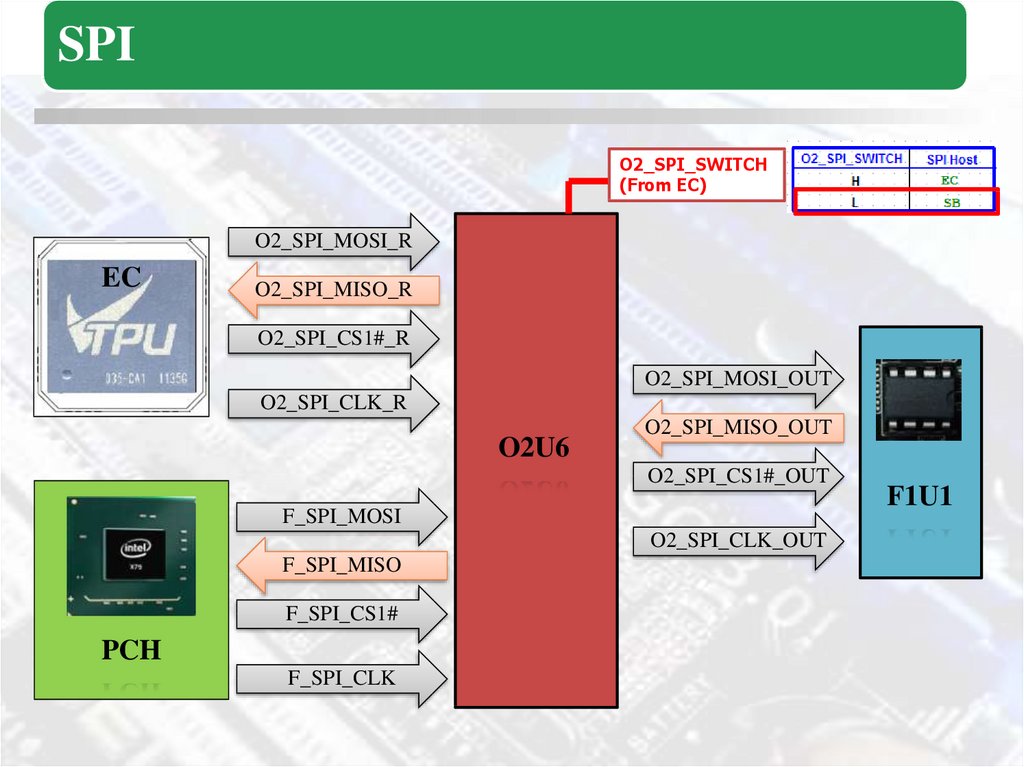
100MHz
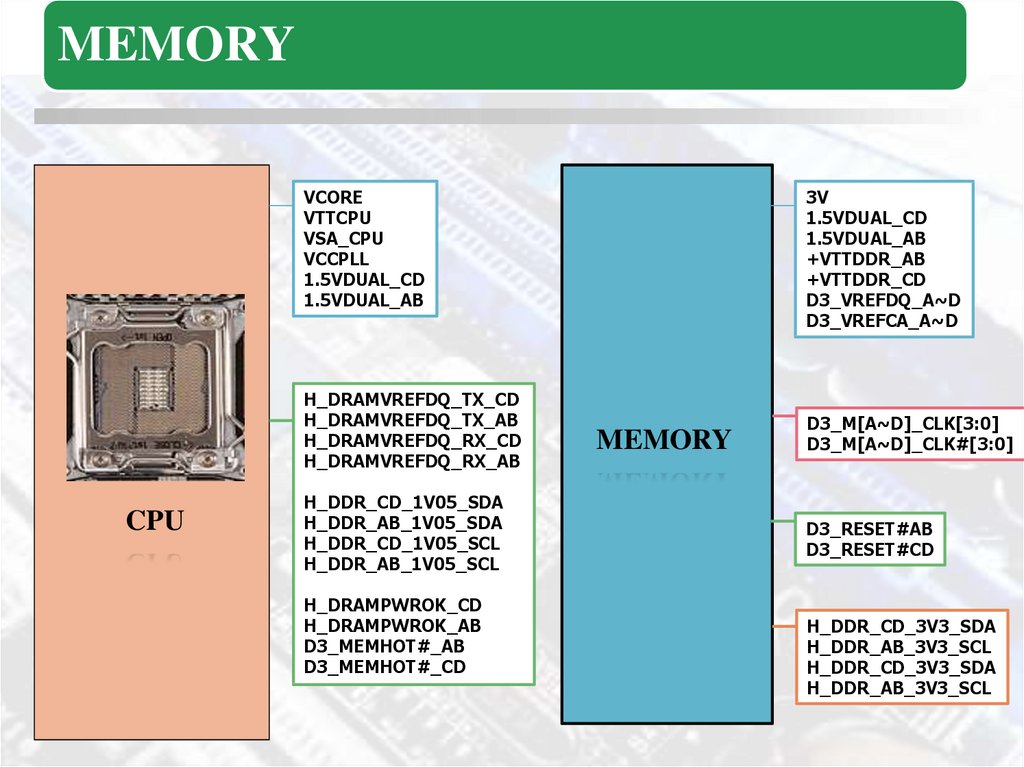
PCI-E X16 SLOT3 (X8)
PCI-E
100MHz
PCI-E X16 SLOT4 (X16/X8)
LGA-2011 Pin Socket
PCI-E
100MHz
ITP
DMI
High-Speed USB
12 ports
480Mb/s
Audio Codec
Realtek ALC898
INTEL
PCIE x1
Intel Lewisville
100MHz
SM BUS
LAN 2
PCIE x1
100MHz
100MHz
PCIE x1
10/100/1000
PCIE x1
Realtek 8111E-VL
Patsburg
100MHz
SM BUS
10/100/1000
100MHz
PCH
33MHz
Q-Switch
PCIE x1
LPC BUS
SIO
NCT6776F
PCIE x1
100MHz
SPI FLASH
32Mb
SPI
PCIE x1
100MHz
PCIE x1
100MHz
100 MHz
CLOCK GEN
96 MHz
ICS
ICS932SQ428AKLF
100 MHz
33MHz
CLOCK GEN
ICS
25 MHz
ICS9FGL1218AKLFT
48MHz
14.318 MHz
SATA0 Gen3
SATA2
SATA4
SATA1 Gen3
SATA3
SATA5
24MHz
Q-Switch
LAN 1
SATA BUS
100 MHz
100 MHz
100 MHz
100 MHz
100 MHz
Marvell
9128
6Gb
ESATA
2 ports
AZAWARE
BT3
PCI-E X1
SLOT1
PCI-E X1
SLOT2
ASM1061
6Gb
PESATA
2 External Ports
ASMEDIA
ASM1042
5Gb/s
USB3.0
Front 2 ports
ASMEDIA
ASM1042
5Gb/s
USB3.0
Back 2 ports
ASMEDIA
ASM1042
5Gb/s
ASMEDIA
VL810
5Gb/s
USB3.0
Back 4 ports
8.
P9X79 PRO - Architecture9.
P9X79 – AgendaIntel X79 Platform Structure
P9X79 Series Architecture
New Feature
Difference With P8 Series
Clock Distribution
Power Flow & Critical Power on X79 Platform
Power Sequence
Embedded Controller Introducing
SIO and Other Power Chipset Introducing
Power theory and working condition
Communication BUS Introducing
10.
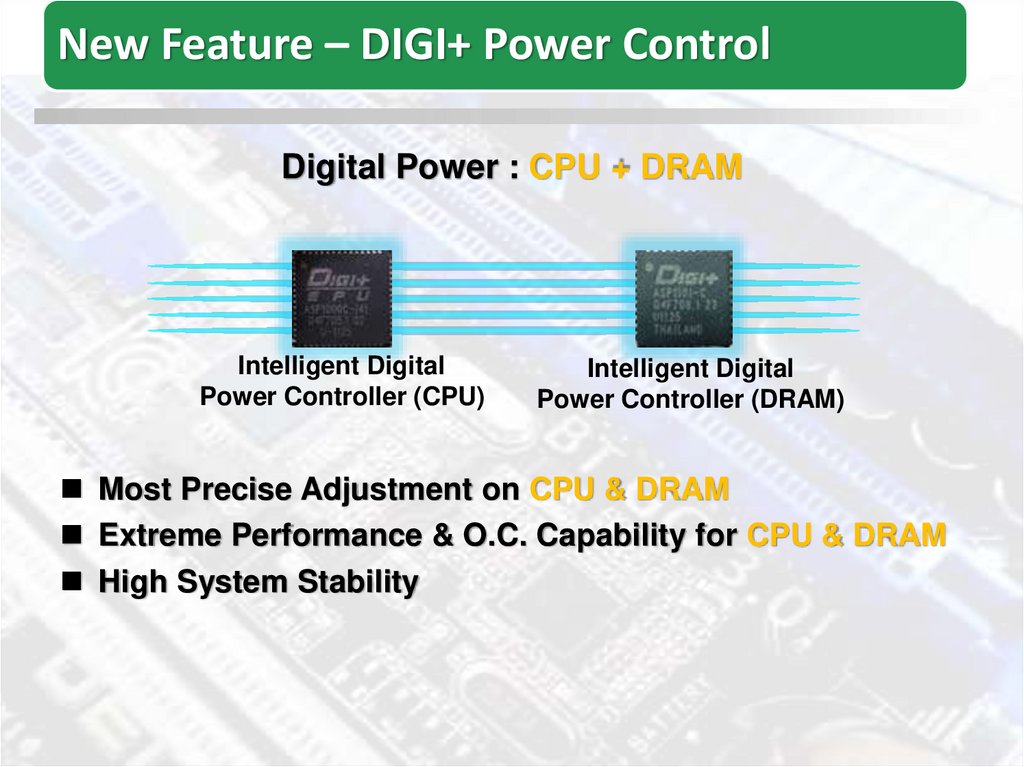
New Feature – DIGI+ Power ControlDIGI+ Power Control
(2/6)
Digital Power : CPU + DRAM
Intelligent Digital
Power Controller (CPU)
Intelligent Digital
Power Controller (DRAM)
Most Precise Adjustment on CPU & DRAM
Extreme Performance & O.C. Capability for CPU & DRAM
High System Stability
11.
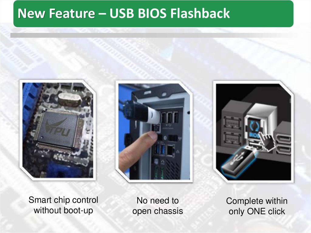
New Feature – USB BIOS FlashbackSmart chip control
without boot-up
No need to
open chassis
Complete within
only ONE click
12.
P9X79 – AgendaIntel X79 Platform Structure
P9X79 Series Architecture
New Feature
Difference With P8 Series
Clock Distribution
Power Flow & Critical Power on X79 Platform
Power Sequence
Embedded Controller Introducing
SIO and Other Power Chipset Introducing
Power theory and working condition
Communication BUS Introducing
13.
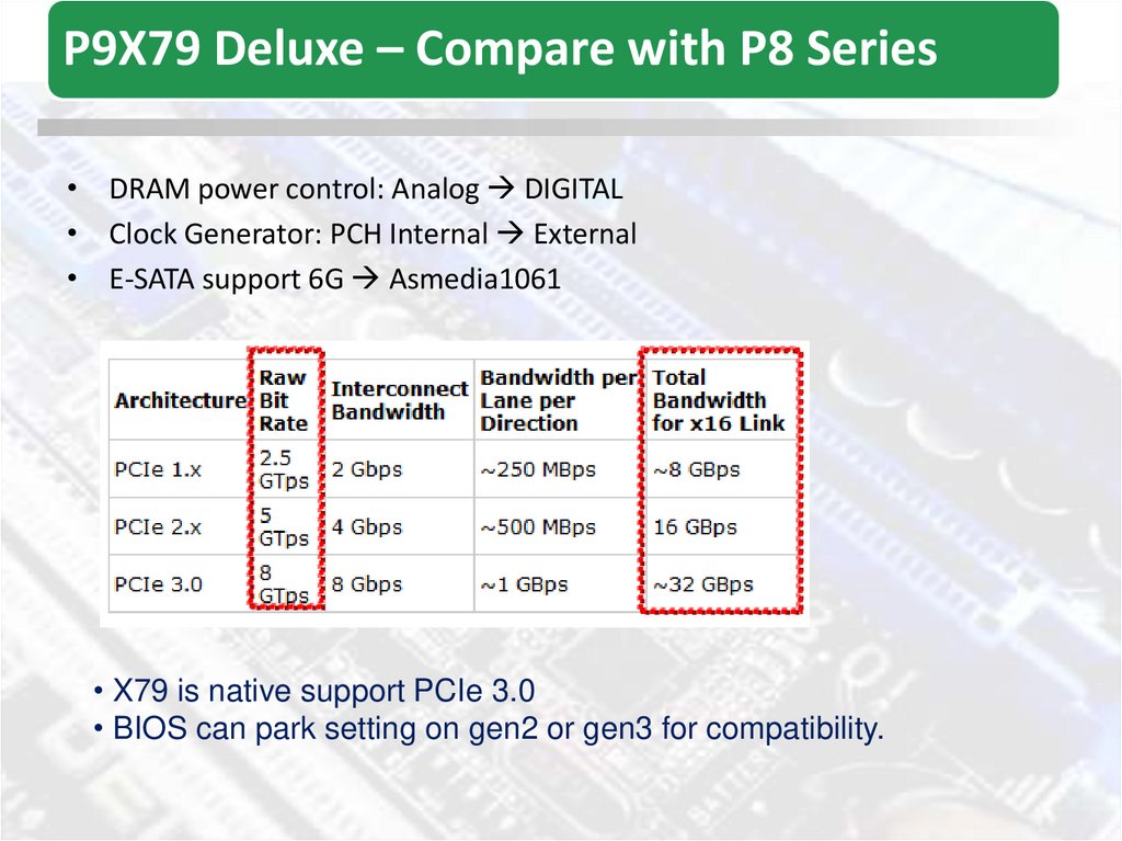
P9X79 Deluxe – Compare with P8 Series• DRAM power control: Analog DIGITAL
• Clock Generator: PCH Internal External
• E-SATA support 6G Asmedia1061
• X79 is native support PCIe 3.0
• BIOS can park setting on gen2 or gen3 for compatibility.
14.
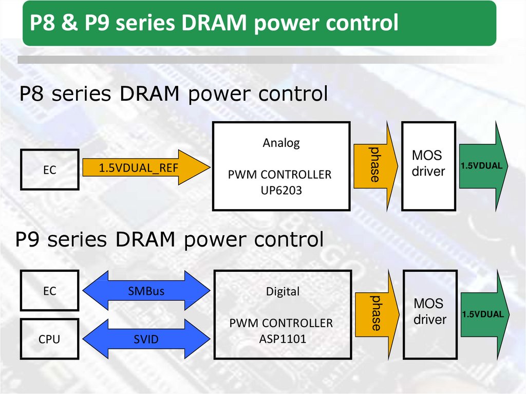
P8 & P9 series DRAM power controlP8 series DRAM power control
1.5VDUAL_REF
PWM CONTROLLER
UP6203
MOS
driver
1.5VDUAL
phase
EC
phase
Analog
MOS
driver
1.5VDUAL
P9 series DRAM power control
EC
CPU
SMBus
SVID
Digital
PWM CONTROLLER
ASP1101
15.
P9X79 – AgendaIntel X79 Platform Structure
P9X79 Series Architecture
New Feature
Difference With P8 Series
Clock Distribution
Power Flow & Critical Power on X79 Platform
Power Sequence
Embedded Controller Introducing
SIO and Other Power Chipset Introducing
Power theory and working condition
Communication BUS Introducing
16.
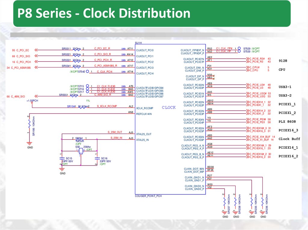
P8 Series - Clock DistributionSU1H
1
C_CLK_PCI4
IPD AT14
CLKOUT_PCI3
CLKOUT_DMI_N
CLKOUT_DMI_P
CLKOUT_PCI4
CLKOUT_DP_N
CLKOUT_DP_P
/X/CPT ST15
/X/CPT ST16
/X/CPT ST17
SR5551 33Ohm 2
66 C_48M_SIO
+1.05PCH
1
1
1
C1_CLK_FLEX0
C1_CLK_FLEX1
C1_CLK_FLEX2
C_48M_SIO_R
IPD AT9
IPD BA5
IPD AW5
IPD BA2
1%
SR1941 90.9Ohm2
S_XCLK_RCOMP
AL2
XCLK_RCOMP
REFCLK14IN
CLOCK
CLKOUT_PCIE0N
CLKOUT_PCIE0P
CLKOUT_PCIE1N
CLKOUT_PCIE1P
CLKOUT_PCIE2N
CLKOUT_PCIE2P
CLKOUT_PCIE3N
CLKOUT_PCIE3P
CLKOUT_PCIE4N
CLKOUT_PCIE4P
S_25M_OUT
S_25M_IN
2 SR501 1
1MOhm
/CPT
SX2 25Mhz
2
1 /CPT
2
SC15
33PF/50V
/CPT
GND
3
AJ3
CLKOUT_PCIE5N
CLKOUT_PCIE5P
XTAL25_OUT
XTAL25_IN
1
1
GND
AJ5
CLKOUT_PCIE6N
CLKOUT_PCIE6P
CLKOUT_PEG_A_N
CLKOUT_PEG_A_P
2
2
SR195 10KOhm
AN8
1
CLKOUTFLEX0/GPIO64
CLKOUTFLEX1/GPIO65
CLKOUTFLEX2/GPIO66
CLKOUTFLEX3/GPIO67
CLKOUT_PEG_B_N
CLKOUT_PEG_B_P
SC16
33PF/50V
/CPT
CLKIN_DOT_96N
CLKIN_DOT_96P
GND
CLKIN_GND1_N
CLKIN_GND1_P
CLKIN_GND0_N
CLKIN_GND0_P
COUGER_POINT_PCH
43
43
9128
C_CPU#
C_CPU
5
5
CPU
C_PCIE_U3#
C_PCIE_U3
48
48
USB3-1
C_PCIE_U3Q# 53
C_PCIE_U3Q 53
USB3-2
C_PCIEX1#_1 32
C_PCIEX1_1 32
PCIEX1_1
C_PCIEX1#_2 32
C_PCIEX1_2 32
PCIEX1_2
C_PCIE_PEX# 58
C_PCIE_PEX 58
PLX 8608
C_PCIEX16#_3 31
C_PCIEX16_3 31
PCIEX16_3
C_PCIE_X1#_BUF 14
C_PCIE_X1_BUF 14
Clock Buff
C_PCIEX16#_1 29
C_PCIEX16_1 29
PCIEX16_1
C_PCIEX16#_2 30
C_PCIEX16_2 30
PCIEX16_2
N56
M55
AE6
AC6
AA5
W5
AB12
AB14
AB9
AB8
Y9
Y8
AF3
AG2
AB3
AA2
AG8
AG9
AE12
AE11
BD38
BF38
R27
P27
W53
V52
GND
GND
GND
SR236 10KOhm
/X/CPT ST542
P31
R31
C_PCIE_R2#
C_PCIE_R2
2
IPD AT17
AE2
AF1
1
C_PCI_ASM1085_R
CLKOUT_PCIE7N
CLKOUT_PCIE7P
CLKOUT_PCI2
ST529 /X/CPT
ST530 /X/CPT
2
SR5541 33Ohm 2
CLKOUT_PCI1
C1_CLK_ITP# 1
C1_CLK_ITP 1
1
IPD AT12
R52
N52
SR235 10KOhm
C_PCI_PCH_R
CLKOUT_ITPXDP_N
CLKOUT_ITPXDP_P
2
SR5531 33Ohm 2
CLKOUT_PCI0
1
IPD AN14
SR238 10KOhm
34 C_PCI_ASM1085
IPD AT11
C_PCI_SIO_R
SR237 10KOhm
16 C_PCI_PCH
C_PCI_EC_R
SR5521 33Ohm 2
2
66 C_PCI_SIO
SR5511 33Ohm 2
1
95 C_PCI_EC
GND
17.
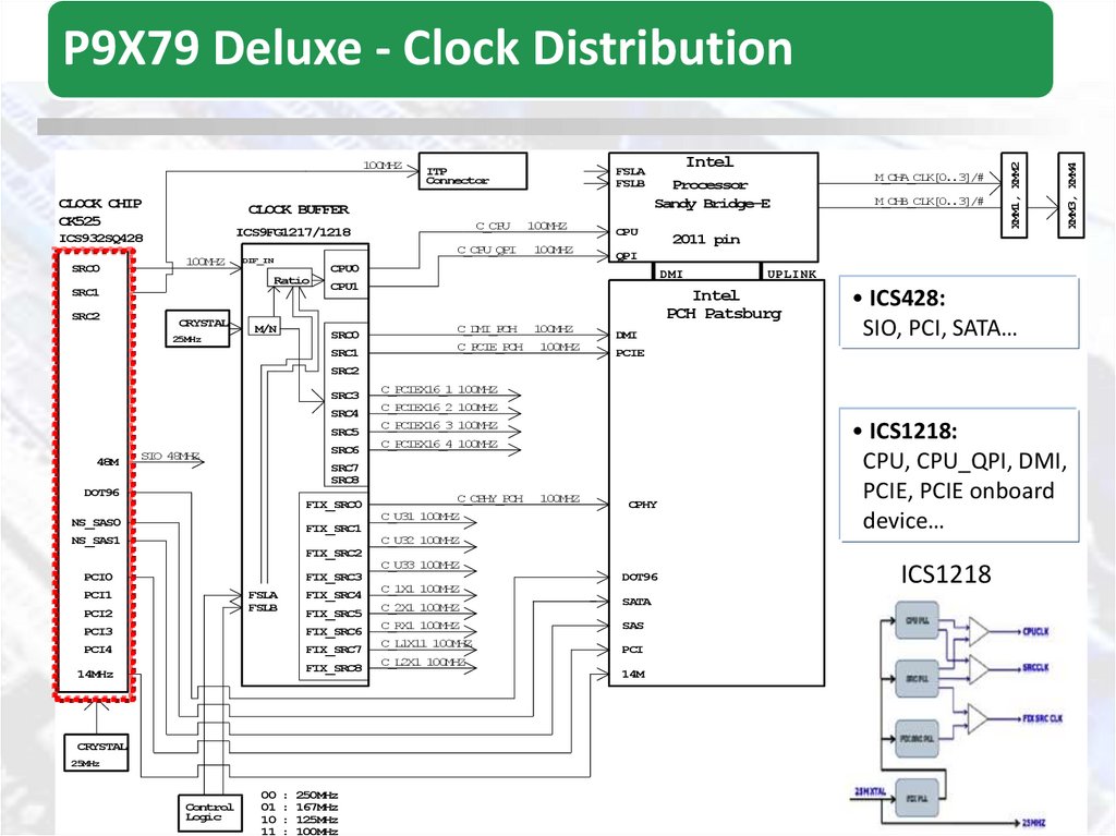
CLOCK CHIPCK525
C_CPU
ICS9FG1217/1218
C_CPU_QPI
100MHZ
DIF_IN
SRC1
CRYSTAL
25MHz
100MHZ
100MHZ
Intel
Processor
Sandy Bridge-E
CPU
M/N
SRC1
UPLINK
Intel
PCH Patsburg
C_DMI_PCH
C_PCIE_PCH
100MHZ
100MHZ
M_CHB_CLK[0..3]/#
2011 pin
DMI
CPU1
SRC0
M_CHA_CLK[0..3]/#
QPI
CPU0
Ratio
SRC2
FSLA
FSLB
CLOCK BUFFER
ICS932SQ428
SRC0
ITP
Connector
XMM3, XMM4
100MHZ
XMM1, XMM2
P9X79 Deluxe - Clock Distribution
DMI
• ICS428:
SIO, PCI, SATA…
PCIE
SRC2
SRC3
SRC4
SRC5
48M
SRC6
SIO 48MHZ
C_PCIEX16_1 100MHZ
C_PCIEX16_2 100MHZ
C_PCIEX16_3 100MHZ
C_PCIEX16_4 100MHZ
SRC7
SRC8
DOT96
FIX_SRC0
C_CPHY_PCH
100MHZ
CPHY
C_U31 100MHZ
NS_SAS0
FIX_SRC1
NS_SAS1
• ICS1218:
CPU, CPU_QPI, DMI,
PCIE, PCIE onboard
device…
C_U32 100MHZ
FIX_SRC2
C_U33 100MHZ
PCI0
FIX_SRC3
PCI1
FSLA
FSLB
PCI2
FIX_SRC4
FIX_SRC5
PCI3
FIX_SRC6
PCI4
FIX_SRC7
FIX_SRC8
14MHz
CRYSTAL
25MHz
Control
Logic
00
01
10
11
:
:
:
:
250MHz
167MHz
125MHz
100MHz
DOT96
C_1X1 100MHZ
C_2X1 100MHZ
C_RX1 100MHZ
C_L1X11 100MHZ
SATA
SAS
PCI
C_L2X1 100MHZ
14M
ICS1218
18.
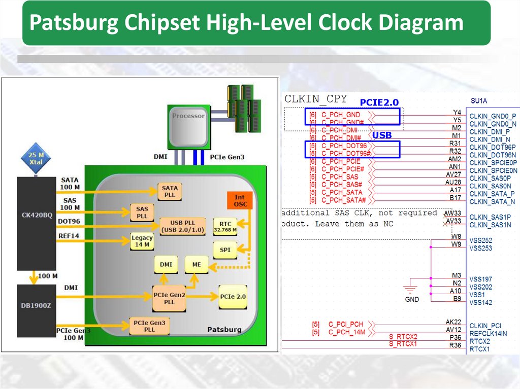
Patsburg Chipset High-Level Clock DiagramPCIE2.0
USB
19.
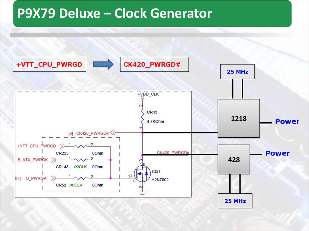
P9X79 Deluxe – Clock Generator+VTT_CPU_PWRGD
CK420_PWRGD#
25 MHz
1218
428
25 MHz
Power
Power
20.
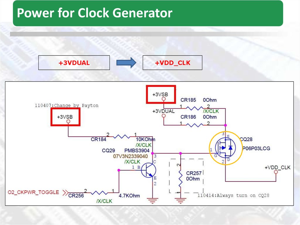
Power for Clock Generator+3VDUAL
+VDD_CLK
21.
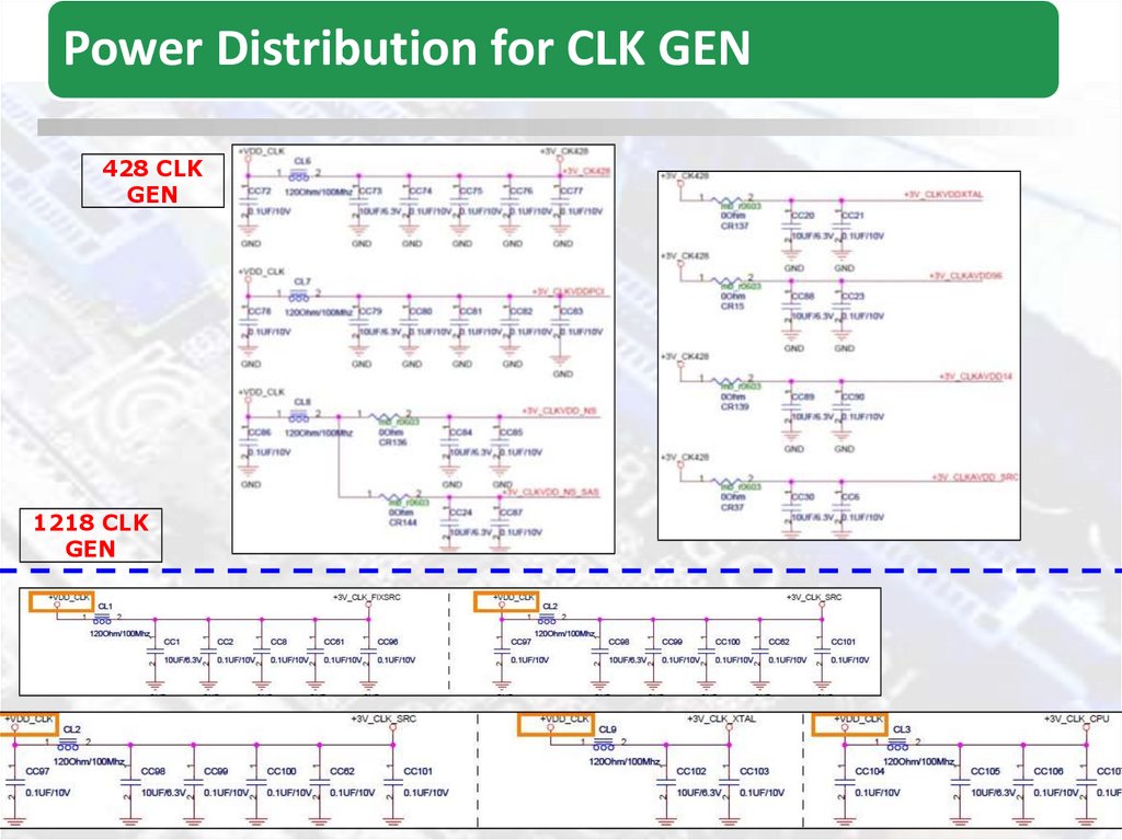
Power Distribution for CLK GEN428 CLK
GEN
1218 CLK
GEN
22.
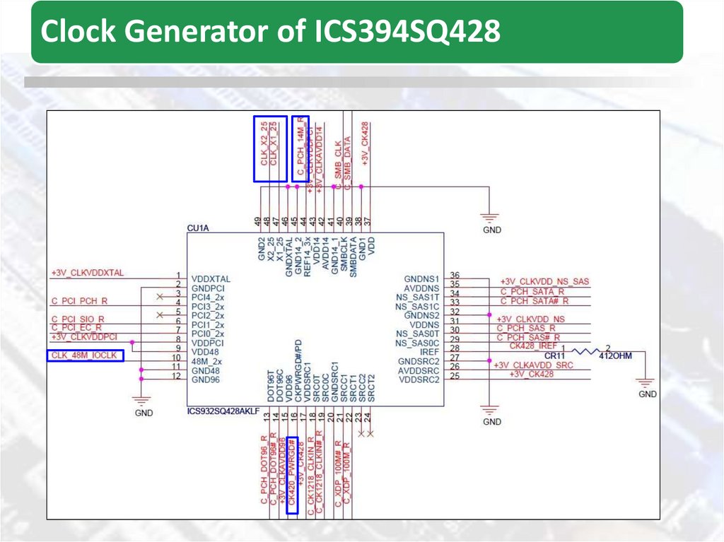
Clock Generator of ICS394SQ42823.
Clock Generator of ICS9FG1218Server MB
(For C_CPU)
SAS
Marvall
9128
(SATA)
C_PCH_GND
(ex: E-SATA)
24.
P9X79 – AgendaIntel X79 Platform Structure
P9X79 Series Architecture
New Feature
Difference With P8 Series
Clock Distribution
Power Flow & Critical Power on X79 Platform
Power Sequence
Embedded Controller Introducing
SIO and Other Power Chipset Introducing
Power theory and working condition
Communication BUS Introducing
25.
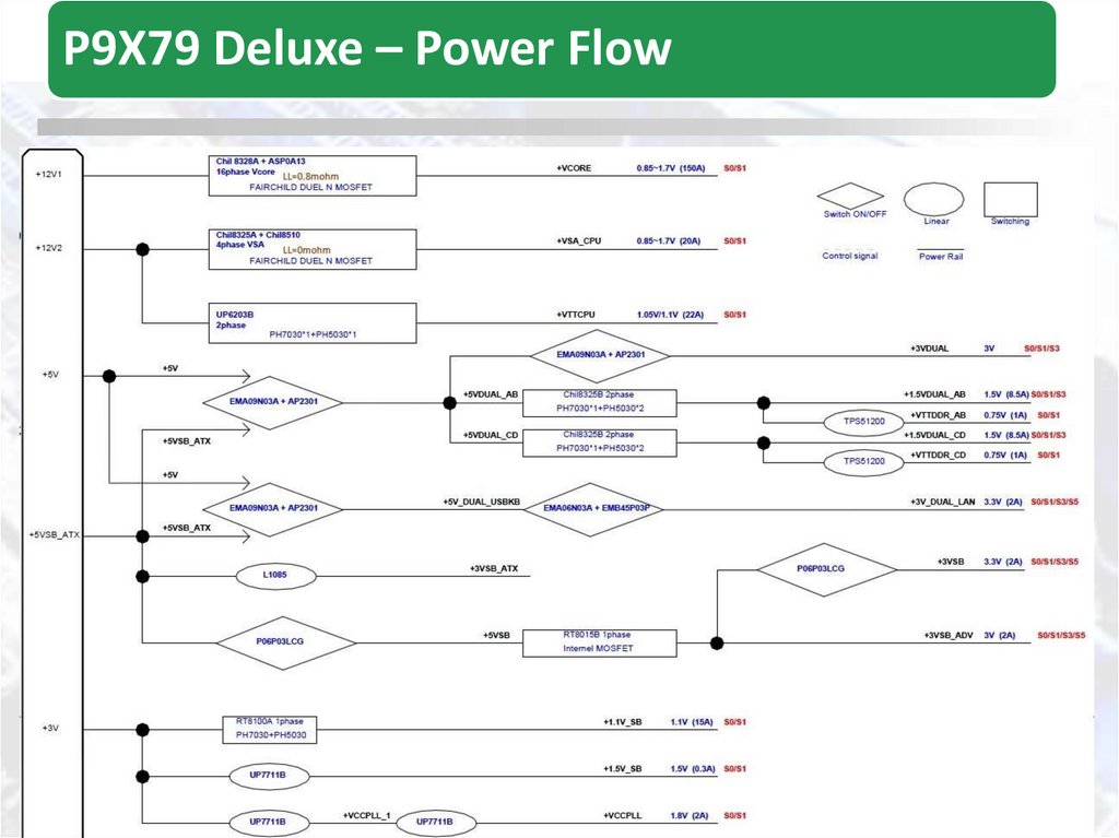
P9X79 Deluxe – Power Flow26.
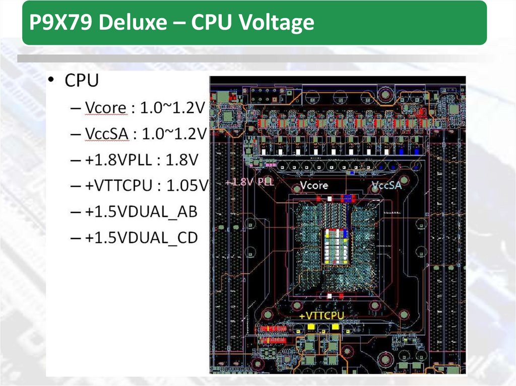
P9X79 Deluxe – CPU Voltage27.
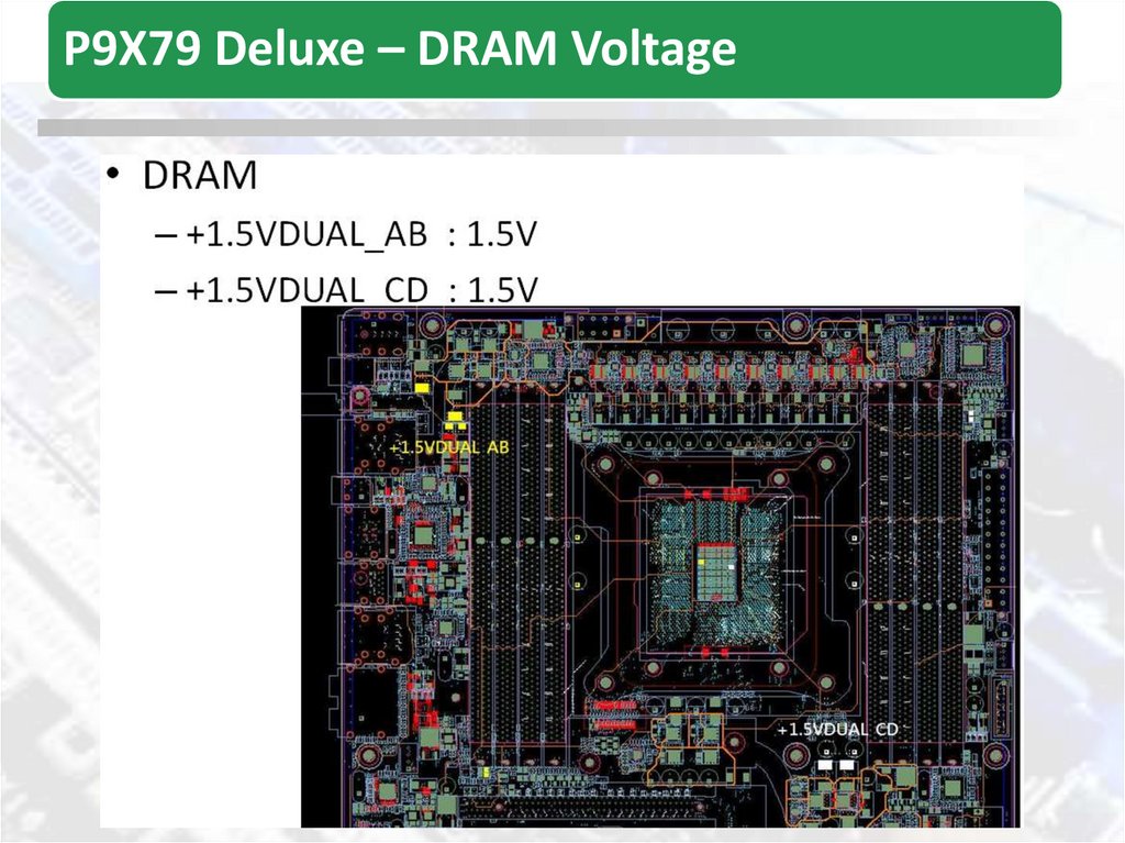
P9X79 Deluxe – DRAM Voltage28.
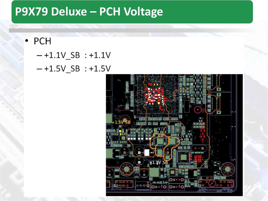
P9X79 Deluxe – PCH Voltage29.
P9X79 – AgendaIntel X79 Platform Structure
P9X79 Series Architecture
New Feature
Difference With P8 Series
Clock Distribution
Power Flow & Critical Power on X79 Platform
Power Sequence
Embedded Controller Introducing
SIO and Other Power Chipset Introducing
Power theory and working condition
Communication BUS Introducing
30.
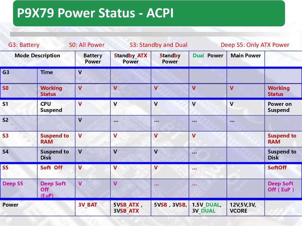
P9X79 Power Status - ACPIG3: Battery
S0: All Power
Mode Description
Battery
Power
S3: Standby and Dual
Standby_ATX
Power
Standby
Power
Deep S5: Only ATX Power
Dual Power
Main Power
G3
Time
V
S0
Working
Status
V
V
V
V
V
Working
Status
S1
CPU
Suspend
V
V
V
V
V
Power on
Suspend
V
…
…
…
…
S2
S3
Suspend to
RAM
V
V
V
V
Suspend to
RAM
S4
Suspend to
Disk
V
V
V
…
Suspend to
Disk
S5
Soft Off
V
V
V
…
SoftOff
Deep S5
Deep Soft
Off
(EuP)
V
V
…
…
Deep Soft
Off EuP
3V_BAT
5VSB_ATX
3VSB_ATX
5VSB 3VSB, 1.5V_DUAL,
3V_DUAL
Power
12V,5V,3V,
VCORE
31.
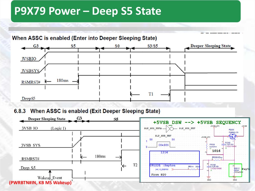
P9X79 Power – Deep S5 State(PWRBTN#IN, KB MS Wakeup)
32.
P9X79 Deluxe - Power Sequence33.
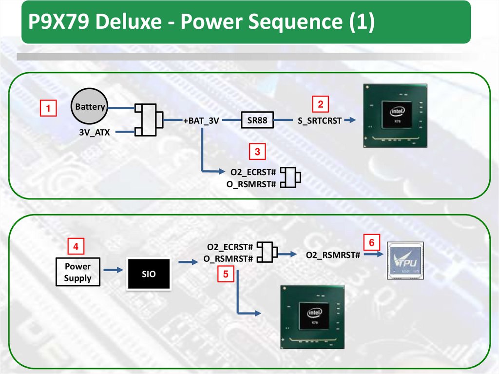
P9X79 Deluxe - Power Sequence (1)1
2
Battery
SR88
+BAT_3V
S_SRTCRST
3V_ATX
3
O2_ECRST#
O_RSMRST#
O2_ECRST#
O_RSMRST#
4
Power
Supply
SIO
5
6
O2_RSMRST#
34.
P9X79 Deluxe - Power Sequence (2)6
O2_ECRST#
O_RSMRST#
O2_RSMRST#
7
P_+VTTCPU_REF
+1.05V level (0.8V in S5)
P_+VCCPLL_REF
+1.8V level (0.03V in S5)
P_+1.1V_SB_REF
+1.1V level
P_+VTTDDR_AB_REF_10 +0.75V level
8
O2_CUT_PSON#
P_+VTTDDR_CD_REF_10 +0.75V level
P_+1.5V_SB_REF_10
O_PSON#
+1.5V level
+3V level
O2_PSON#
+3V level
35.
P9X79 Deluxe - Power Sequence (3)Power
Button
9
10
O_PWRBTN#IN
SIO
O_PWRBTN#
12
SLP_S3#
SLP_S4#
11
SIO
13
O_PSON#
O2_PSON#
O2_CUT_PSON#
13
O2_PSON#
14
Power
Supply
3V, 5V, 12V
+3V level
+3V level
+3V level
15
Power
Supply
B_ATX_PWROK
SIO
+5V level
+5V level
+3V level
36.
P9X79 Deluxe - Power Sequence (4)+VTT_CPU, +1.5VDUAL_AB, +1.5VDUAL_CD, +1.1V_SB, +1.5V_SB
16
+1.05V level
+1.5VDUAL_CD
17
IC
18
+VTT_CPU
+1.5V level
+1.5V level
+1.1V level
+1.5V level
SR1478
+VDDQ_AB_PWRGD
S_DRAMPWROK
H_DRAMPWROK_AB
+VDDQ_CD_PWRGD
S_DRAMPWROK
H_DRAMPWROK_CD
MB Logic
Circuit
+VTT_CPU_PWRGD
+1.5V level
+3V level
37.
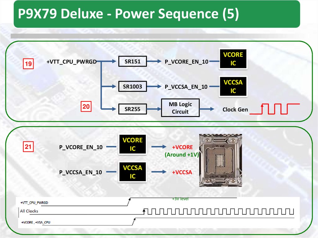
P9X79 Deluxe - Power Sequence (5)19
+VTT_CPU_PWRGD
20
21
SR151
P_VCORE_EN_10
VCORE
IC
SR1003
P_VCCSA_EN_10
VCCSA
IC
SR255
P_VCORE_EN_10
VCORE
IC
P_VCCSA_EN_10
VCCSA
IC
MB Logic
Circuit
+VCORE
(Around +1V)
+VCCSA
+3V level
Clock Gen
38.
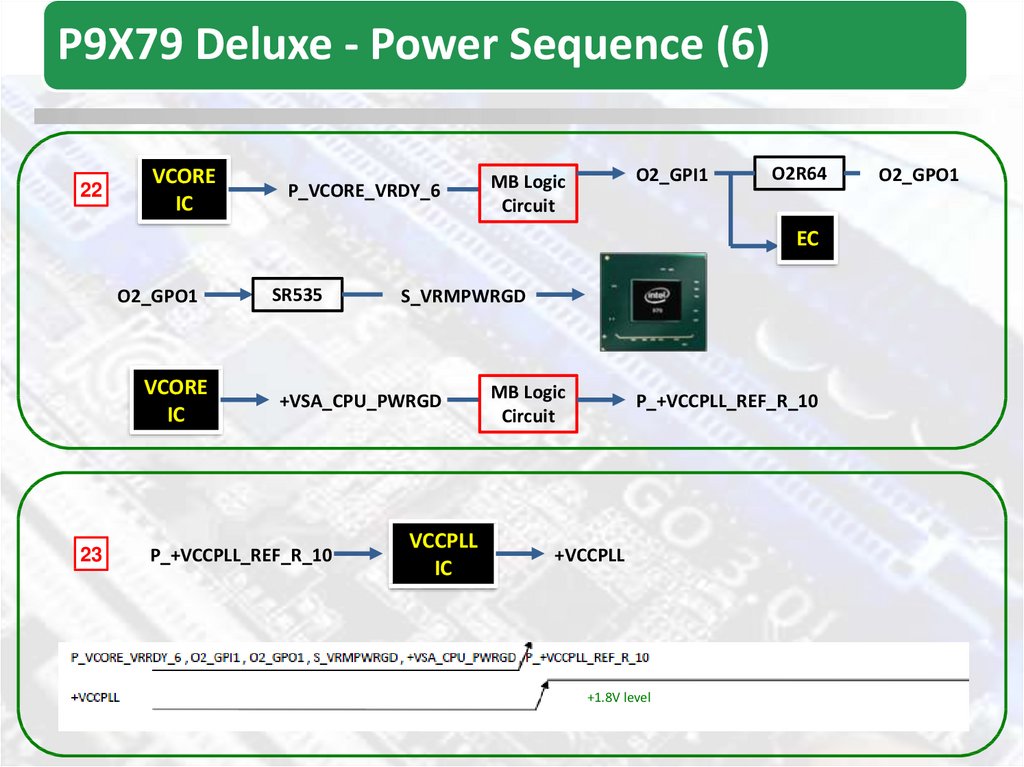
P9X79 Deluxe - Power Sequence (6)22
VCORE
IC
P_VCORE_VRDY_6
O2_GPI1
MB Logic
Circuit
O2R64
EC
O2_GPO1
VCORE
IC
23
SR535
S_VRMPWRGD
+VSA_CPU_PWRGD
P_+VCCPLL_REF_R_10
VCCPLL
IC
MB Logic
Circuit
P_+VCCPLL_REF_R_10
+VCCPLL
+1.8V level
O2_GPO1
39.
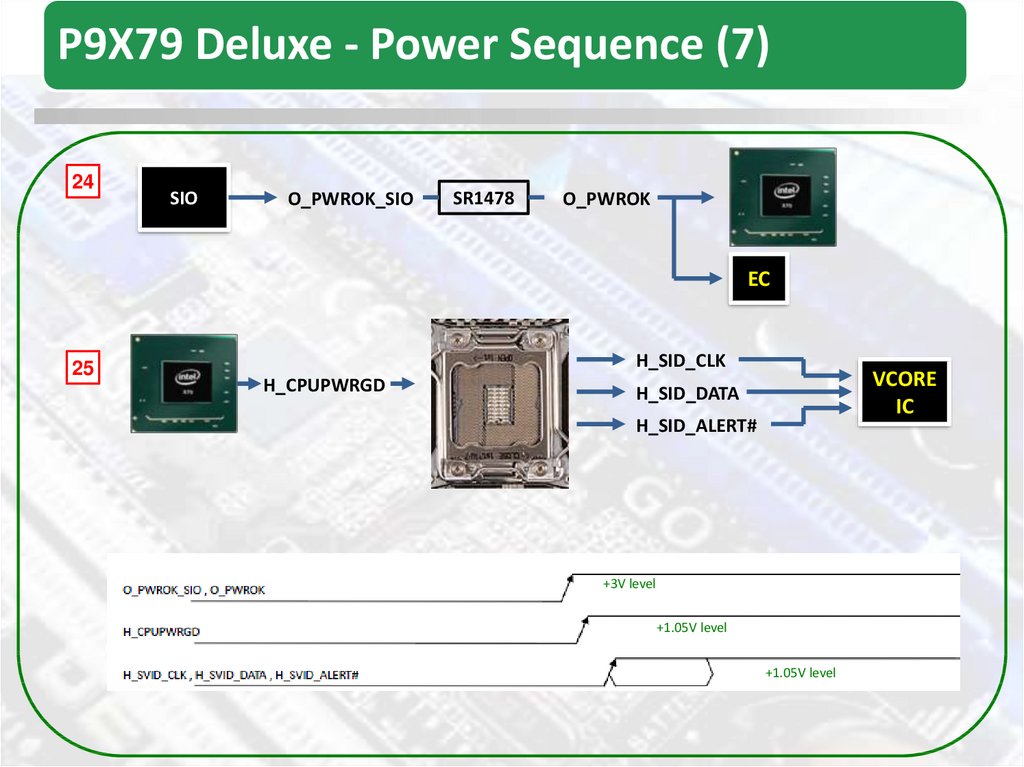
P9X79 Deluxe - Power Sequence (7)24
SIO
O_PWROK_SIO
SR1478
O_PWROK
EC
25
H_SID_CLK
H_CPUPWRGD
VCORE
IC
H_SID_DATA
H_SID_ALERT#
+3V level
+1.05V level
+1.05V level
40.
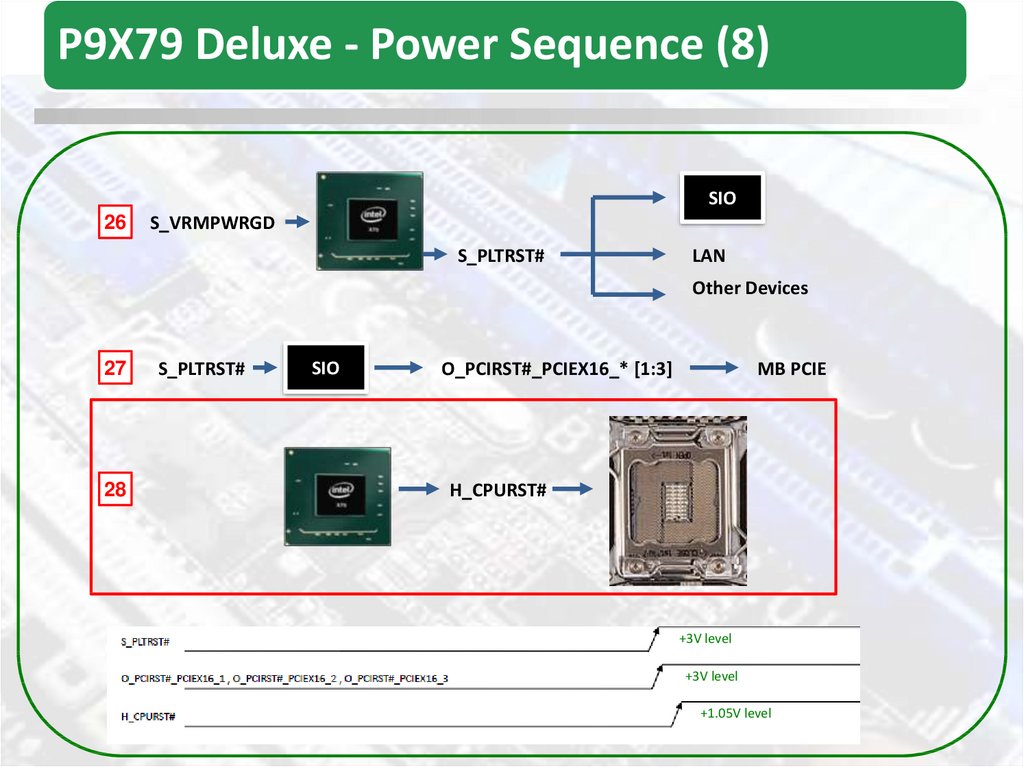
P9X79 Deluxe - Power Sequence (8)SIO
26
S_VRMPWRGD
S_PLTRST#
LAN
Other Devices
27
28
S_PLTRST#
SIO
O_PCIRST#_PCIEX16_* [1:3]
MB PCIE
H_CPURST#
+3V level
+3V level
+1.05V level
41.
P9X79 – AgendaIntel X79 Platform Structure
P9X79 Series Architecture
New Feature
Difference With P8 Series
Clock Distribution
Power Flow & Critical Power on X79 Platform
Power Sequence
Embedded Controller Introducing
SIO and Other Power Chipset Introducing
Power theory and working condition
Communication BUS Introducing
42.
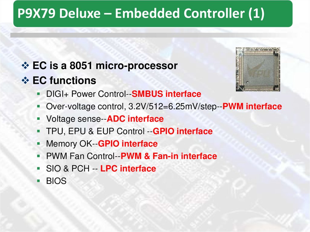
P9X79 Deluxe – Embedded Controller (1)EC is a 8051 micro-processor
EC functions
DIGI+ Power Control--SMBUS interface
Over-voltage control, 3.2V/512=6.25mV/step--PWM interface
Voltage sense--ADC interface
TPU, EPU & EUP Control --GPIO interface
Memory OK--GPIO interface
PWM Fan Control--PWM & Fan-in interface
SIO & PCH -- LPC interface
BIOS
43.
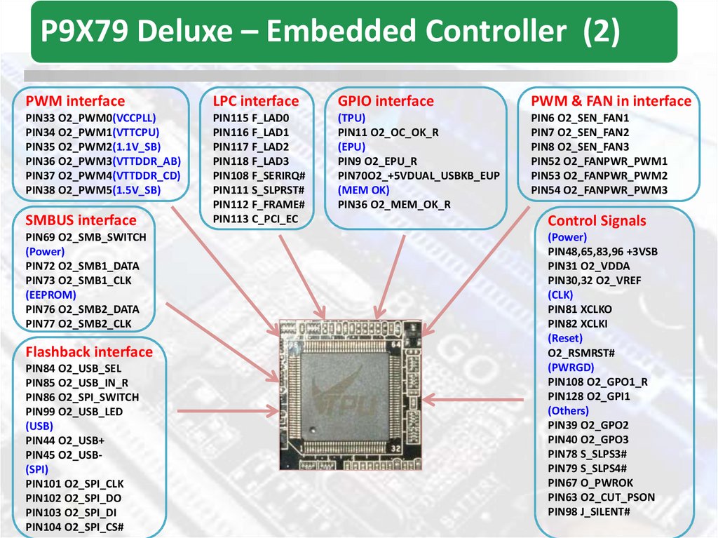
P9X79 Deluxe – Embedded Controller (2)PWM interface
LPC interface
GPIO interface
PWM & FAN in interface
PIN33 O2_PWM0(VCCPLL)
PIN34 O2_PWM1(VTTCPU)
PIN35 O2_PWM2(1.1V_SB)
PIN36 O2_PWM3(VTTDDR_AB)
PIN37 O2_PWM4(VTTDDR_CD)
PIN38 O2_PWM5(1.5V_SB)
PIN115 F_LAD0
PIN116 F_LAD1
PIN117 F_LAD2
PIN118 F_LAD3
PIN108 F_SERIRQ#
PIN111 S_SLPRST#
PIN112 F_FRAME#
PIN113 C_PCI_EC
(TPU)
PIN11 O2_OC_OK_R
(EPU)
PIN9 O2_EPU_R
PIN70O2_+5VDUAL_USBKB_EUP
(MEM OK)
PIN36 O2_MEM_OK_R
PIN6 O2_SEN_FAN1
PIN7 O2_SEN_FAN2
PIN8 O2_SEN_FAN3
PIN52 O2_FANPWR_PWM1
PIN53 O2_FANPWR_PWM2
PIN54 O2_FANPWR_PWM3
SMBUS interface
PIN69 O2_SMB_SWITCH
(Power)
PIN72 O2_SMB1_DATA
PIN73 O2_SMB1_CLK
(EEPROM)
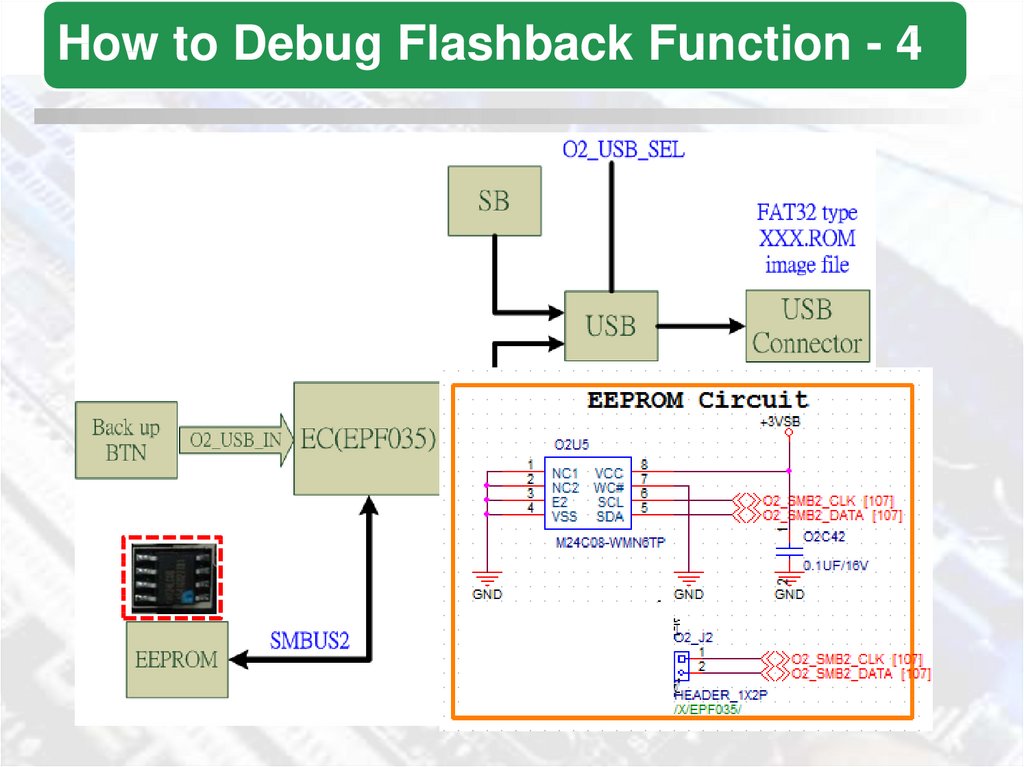
PIN76 O2_SMB2_DATA
PIN77 O2_SMB2_CLK
Flashback interface
PIN84 O2_USB_SEL
PIN85 O2_USB_IN_R
PIN86 O2_SPI_SWITCH
PIN99 O2_USB_LED
(USB)
PIN44 O2_USB+
PIN45 O2_USB(SPI)
PIN101 O2_SPI_CLK
PIN102 O2_SPI_DO
PIN103 O2_SPI_DI
PIN104 O2_SPI_CS#
Control Signals
(Power)
PIN48,65,83,96 +3VSB
PIN31 O2_VDDA
PIN30,32 O2_VREF
(CLK)
PIN81 XCLKO
PIN82 XCLKI
(Reset)
O2_RSMRST#
(PWRGD)
PIN108 O2_GPO1_R
PIN128 O2_GPI1
(Others)
PIN39 O2_GPO2
PIN40 O2_GPO3
PIN78 S_SLPS3#
PIN79 S_SLPS4#
PIN67 O_PWROK
PIN63 O2_CUT_PSON
PIN98 J_SILENT#
44.
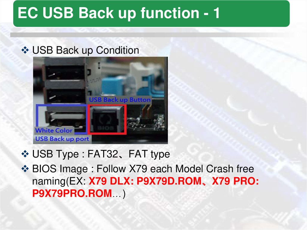
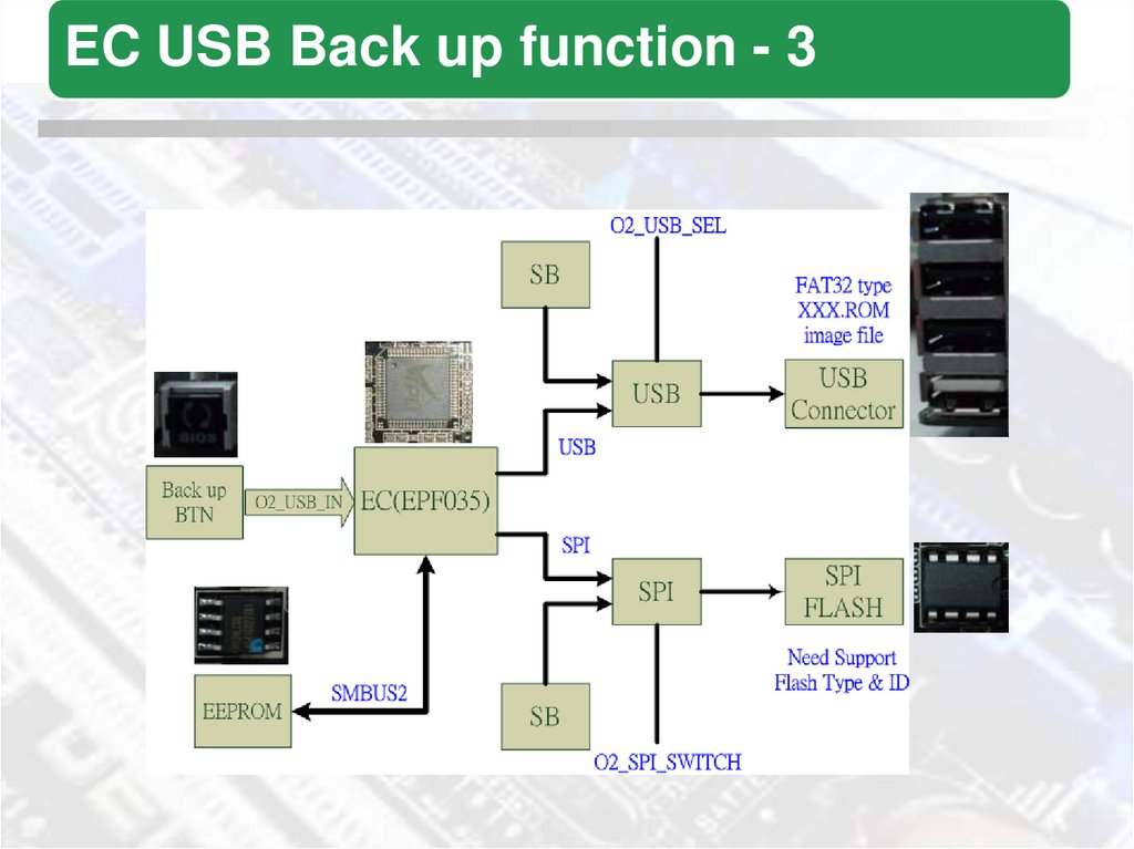
EC USB Back up function - 1USB Back up Condition
USB Type : FAT32、FAT type
BIOS Image : Follow X79 each Model Crash free
naming(EX: X79 DLX: P9X79D.ROM、X79 PRO:
P9X79PRO.ROM…)
45.
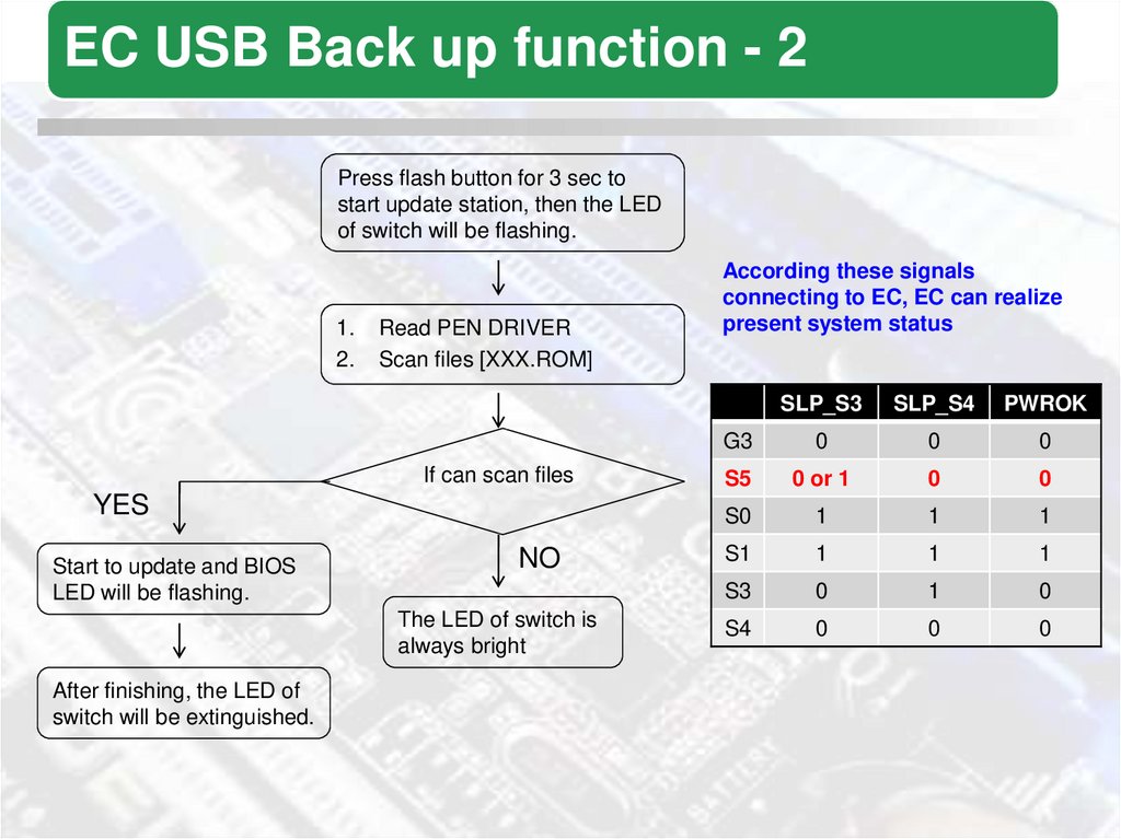
EC USB Back up function - 2Press flash button for 3 sec to
start update station, then the LED
of switch will be flashing.
1.
2.
Read PEN DRIVER
Scan files [XXX.ROM]
If can scan files
YES
Start to update and BIOS
LED will be flashing.
NO
The LED of switch is
always bright
After finishing, the LED of
switch will be extinguished.
According these signals
connecting to EC, EC can realize
present system status
SLP_S3
SLP_S4
PWROK
G3
0
0
0
S5
0 or 1
0
0
S0
1
1
1
S1
1
1
1
S3
0
1
0
S4
0
0
0
46.
EC USB Back up function - 347.
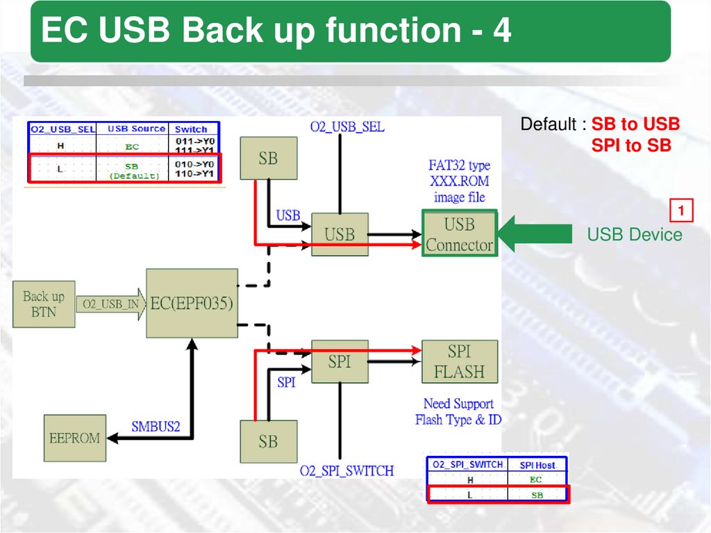
EC USB Back up function - 4Default : SB to USB
SPI to SB
1
USB Device
48.
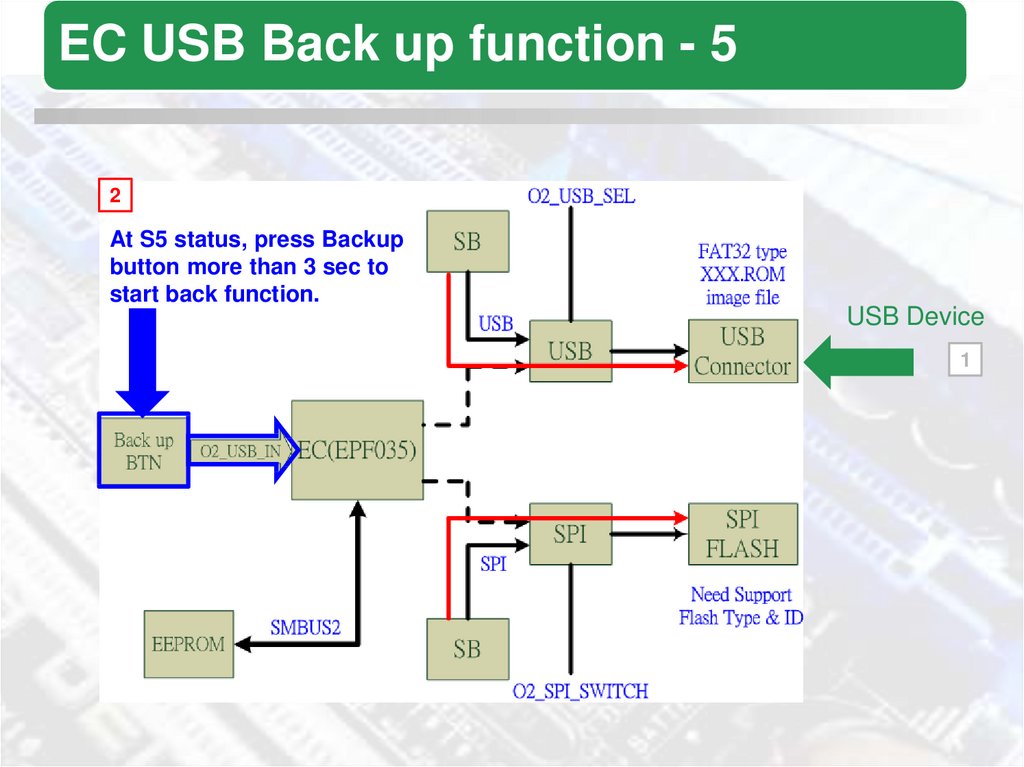
EC USB Back up function - 52
At S5 status, press Backup
button more than 3 sec to
start back function.
USB Device
1
49.
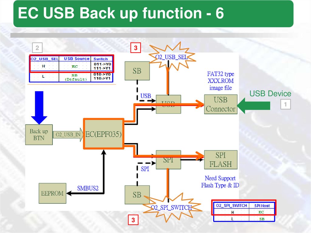
EC USB Back up function - 62
3
2
USB Device
1
3
50.
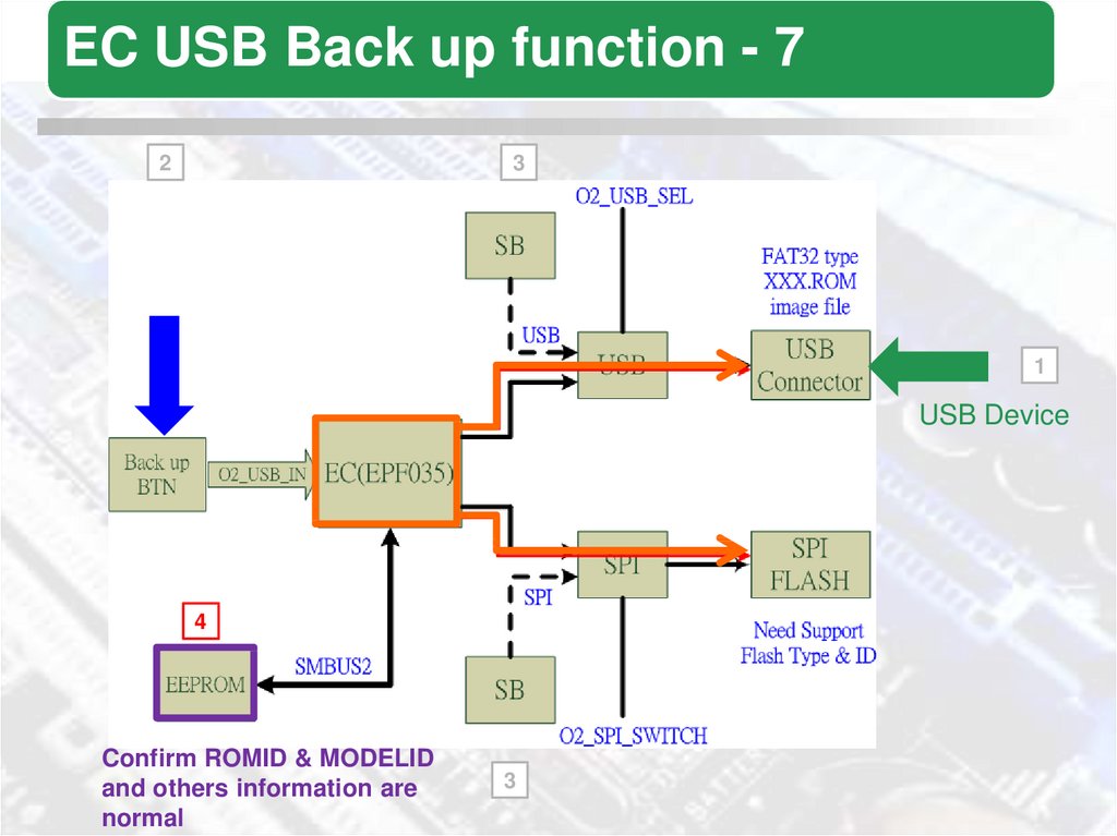
EC USB Back up function - 72
3
1
USB Device
4
Confirm ROMID & MODELID
and others information are
normal
3
51.
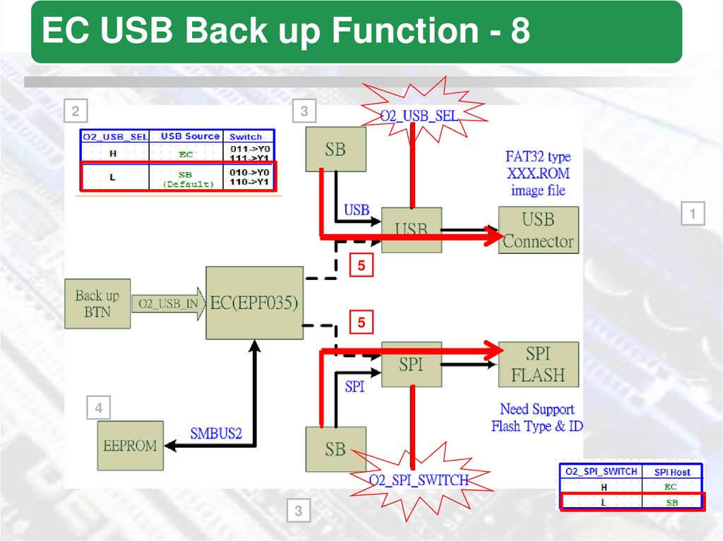
EC USB Back up Function - 82
3
1
5
5
4
3
52.
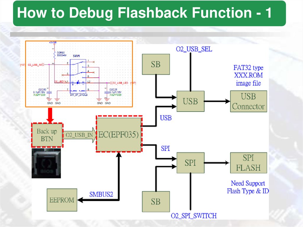
How to Debug Flashback Function - 153.
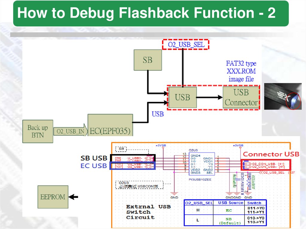
How to Debug Flashback Function - 254.
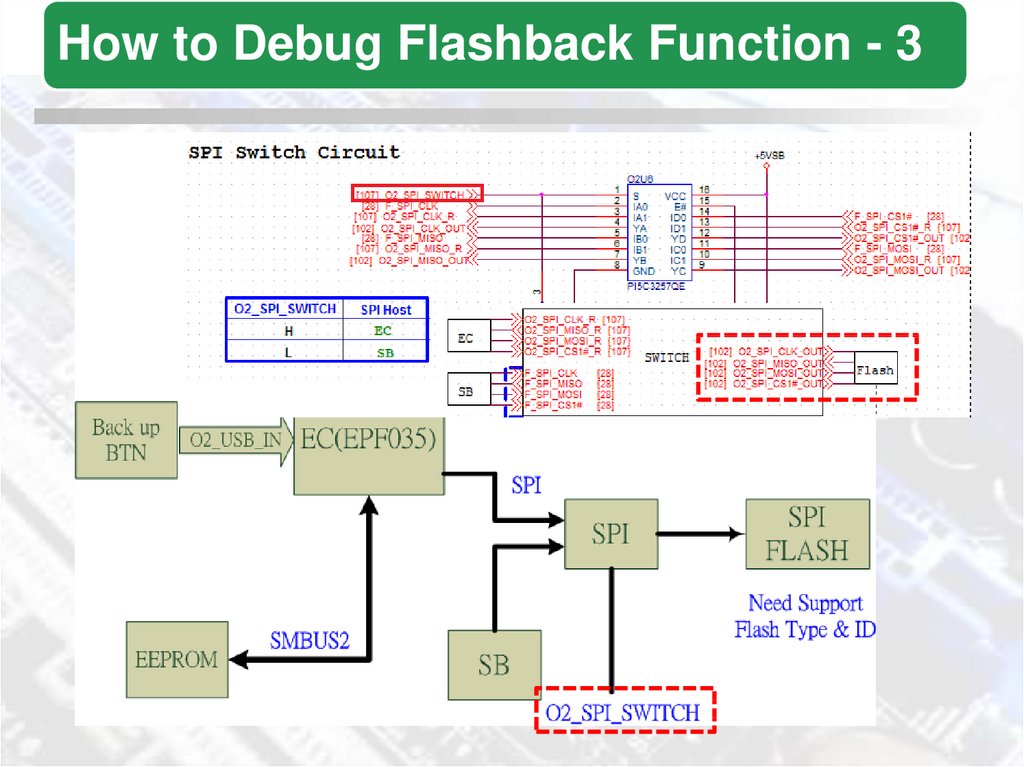
How to Debug Flashback Function - 355.
How to Debug Flashback Function - 456.
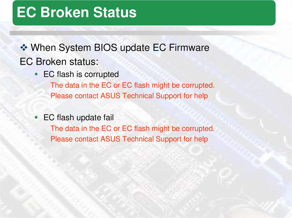
EC Broken StatusWhen System BIOS update EC Firmware
EC Broken status:
EC flash is corrupted
The data in the EC or EC flash might be corrupted.
Please contact ASUS Technical Support for help
EC flash update fail
The data in the EC or EC flash might be corrupted.
Please contact ASUS Technical Support for help
57.
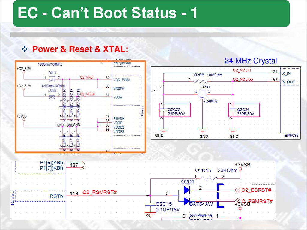
EC - Can’t Boot Status - 1Power & Reset & XTAL:
24 MHz Crystal
58.
EC - Can’t Boot Status - 2O2_OP_mode:
This PIN is used for RD & factory to update EC firmware or flash programming.
Normal should always keep low.
59.
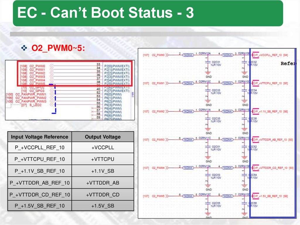
EC - Can’t Boot Status - 3O2_PWM0~5:
Input Voltage Reference
Output Voltage
P_+VCCPLL_REF_10
+VCCPLL
P_+VTTCPU_REF_10
+VTTCPU
P_+1.1V_SB_REF_10
+1.1V_SB
P_+VTTDDR_AB_REF_10
+VTTDDR_AB
P_+VTTDDR_CD_REF_10
+VTTDDR_CD
P_+1.5V_SB_REF_10
+1.5V_SB
60.
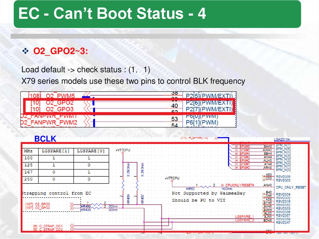
EC - Can’t Boot Status - 4O2_GPO2~3:
Load default -> check status : (1 1)
X79 series models use these two pins to control BLK frequency
BCLK
61.
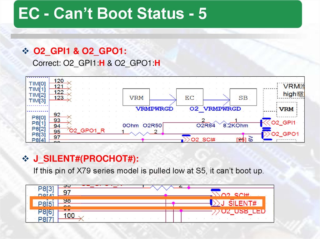
EC - Can’t Boot Status - 5O2_GPI1 & O2_GPO1:
Correct: O2_GPI1:H & O2_GPO1:H
J_SILENT#(PROCHOT#):
If this pin of X79 series model is pulled low at S5, it can’t boot up.
62.
EC - Can’t Boot Status - 6O_PWRBTN#IN_R& O_RSTCON#: Can’t Keep Low
O2_CUT_PSON#: To keep PWRBTN motion
AC Power On -> PWM signal ready -> O2_CUT_PSON#: H
When starting to USB BIOS flashback, this pin is also low.
63.
EC - Hang 0d0c StatusSMBUS & O2_SMB_SWITCH:
Hang”0d0c” : EC check internal register setting of each DIGI+ Power Control.
64.
P9X79 – AgendaIntel X79 Platform Structure
P9X79 Series Architecture
New Feature
Difference With P8 Series
Clock Distribution
Power Flow & Critical Power on X79 Platform
Power Sequence
Embedded Controller Introducing
SIO and Other Power Chipset Introducing
Power theory and working condition
Communication BUS Introducing
65.
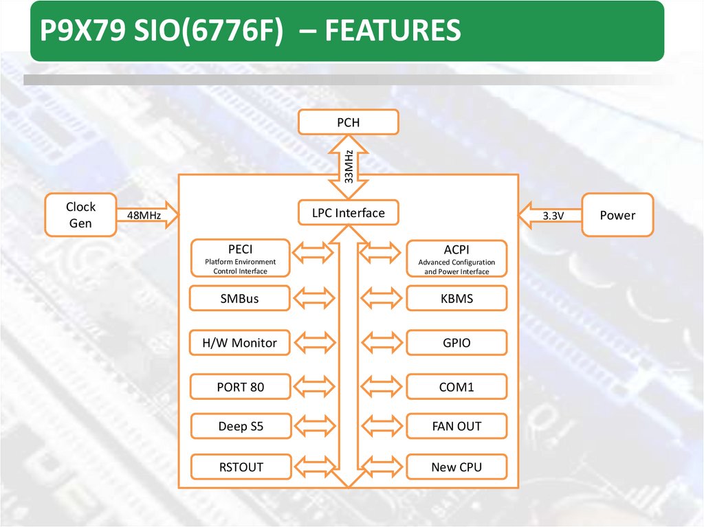
P9X79 SIO(6776F) – FEATURES33MHz
PCH
Clock
Gen
LPC Interface
48MHz
3.3V
PECI
ACPI
Platform Environment
Control Interface
Advanced Configuration
and Power Interface
SMBus
KBMS
H/W Monitor
GPIO
PORT 80
COM1
Deep S5
FAN OUT
RSTOUT
New CPU
Power
66.
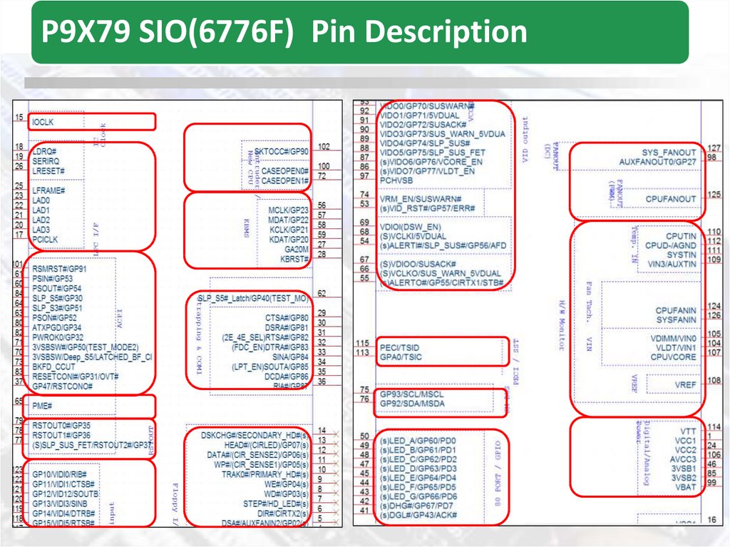
P9X79 SIO(6776F) Pin Description67.
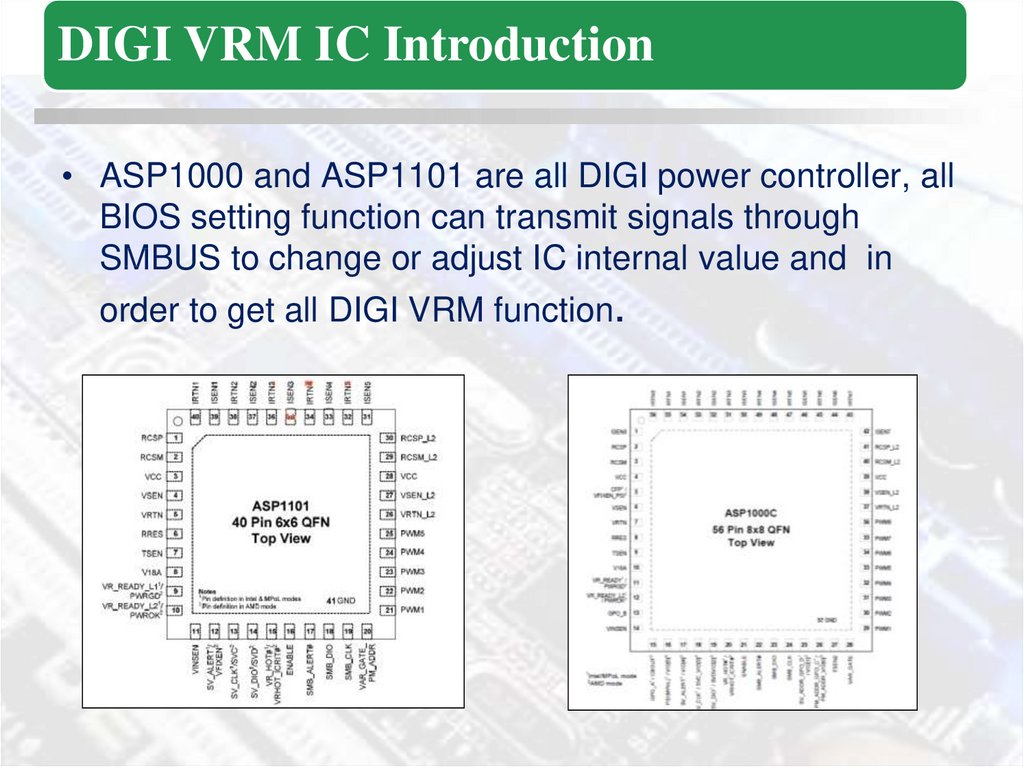
DIGI VRM IC Introduction• ASP1000 and ASP1101 are all DIGI power controller, all
BIOS setting function can transmit signals through
SMBUS to change or adjust IC internal value and in
order to get all DIGI VRM function.
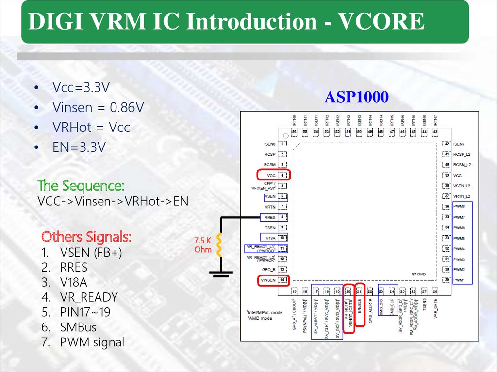
68.
DIGI VRM IC Introduction - VCOREVcc=3.3V
Vinsen = 0.86V
VRHot = Vcc
EN=3.3V
ASP1000
The Sequence:
VCC->Vinsen->VRHot->EN
Others Signals:
1.
2.
3.
4.
5.
6.
7.
VSEN (FB+)
RRES
V18A
VR_READY
PIN17~19
SMBus
PWM signal
7.5 K
Ohm
69.
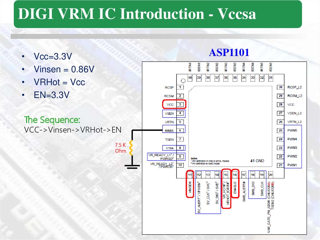
DIGI VRM IC Introduction - VccsaASP1101
Vcc=3.3V
Vinsen = 0.86V
VRHot = Vcc
EN=3.3V
The Sequence:
VCC->Vinsen->VRHot->EN
7.5 K
Ohm
70.
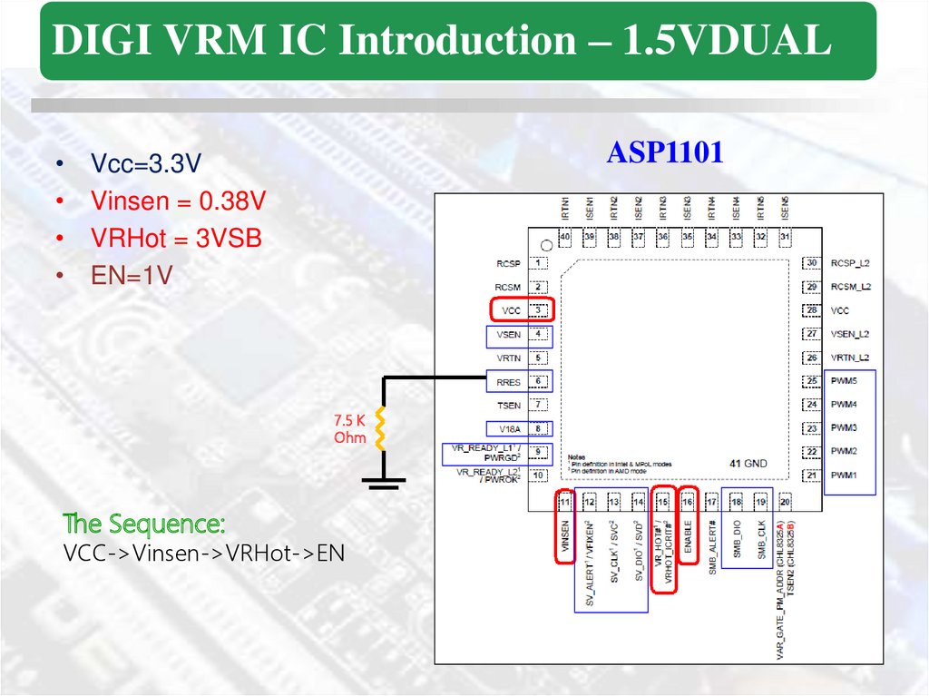
DIGI VRM IC Introduction – 1.5VDUALASP1101
Vcc=3.3V
Vinsen = 0.38V
VRHot = 3VSB
EN=1V
7.5 K
Ohm
The Sequence:
VCC->Vinsen->VRHot->EN
71.
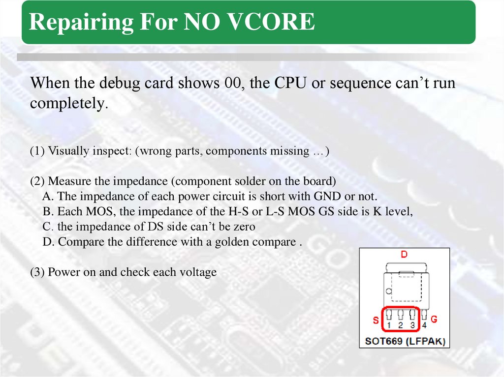
Repairing For NO VCOREWhen the debug card shows 00, the CPU or sequence can’t run
completely.
(1) Visually inspect: (wrong parts, components missing …)
(2) Measure the impedance (component solder on the board)
A. The impedance of each power circuit is short with GND or not.
B. Each MOS, the impedance of the H-S or L-S MOS GS side is K level,
C. the impedance of DS side can’t be zero
D. Compare the difference with a golden compare .
(3) Power on and check each voltage
72.
How To Identify MOS Is NormalStep 1:
Multi-meter in Ω level : “+” side connects with Source, “-” side connects with
Gate. Let MOSFET going into the cut-off state.
Step 2:
Multi-meter in diode level : “+” side connects with Source, “-” side connects
with drain, measure Vf: 0.3V ~ 0.6V
Step 3:
Multi-meter in resistance level :
“+” side connects with drain, “-” side connects with source Value: xM Ω, ~ ∞ Ω,
“+” side connects with drain, “-” side connects with gate Value: xM Ω, ~ ∞ Ω
“+” side connects with source, “-” side connects with gate Value: xM Ω, ~ ∞ Ω
Step 4:
Multi-meter in resistance level :
“+” side connects with gate, “-” side connects with source ,to turn on MOSFET
“+” side connects with drain, “-” side connects with source Value: 0Ω ~~ 10 Ω
73.
P9X79 – AgendaIntel X79 Platform Structure
P9X79 Series Architecture
New Feature
Difference With P8 Series
Clock Distribution
Power Flow & Critical Power on X79 Platform
Power Sequence
Embedded Controller Introducing
SIO and Other Power Chipset Introducing
Power theory and working condition
Communication BUS Introducing
74.
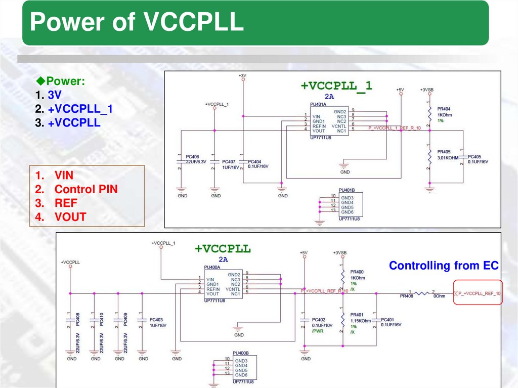
Power of VCCPLLPower:
1. 3V
2. +VCCPLL_1
3. +VCCPLL
1.
2.
3.
4.
VIN
Control PIN
REF
VOUT
Controlling from EC
75.
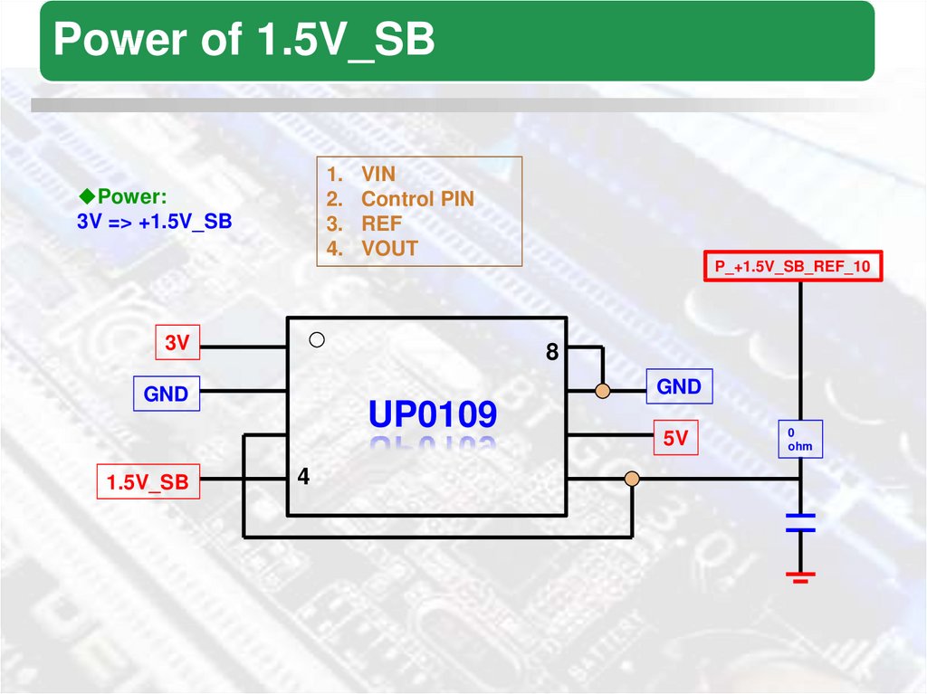
Power of 1.5V_SB1.
2.
3.
4.
Power:
3V => +1.5V_SB
VIN
Control PIN
REF
VOUT
P_+1.5V_SB_REF_10
3V
8
GND
GND
1.5V_SB
UP0109
4
5V
0
ohm
76.
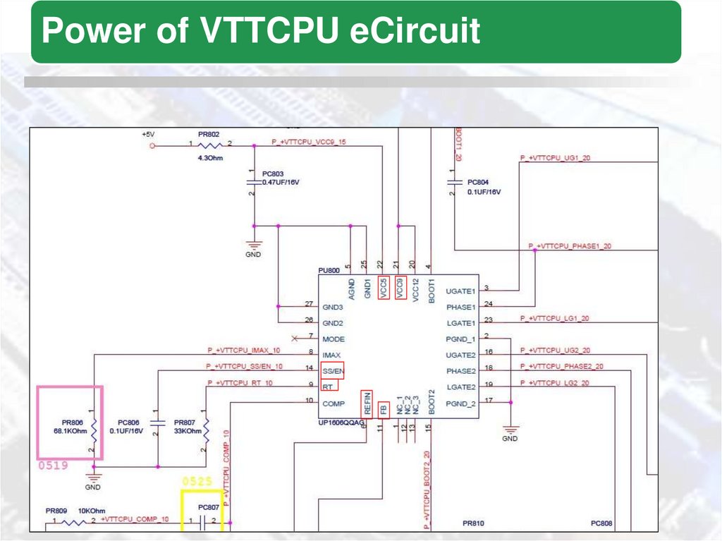
Power of VTTCPU eCircuit+d
77.
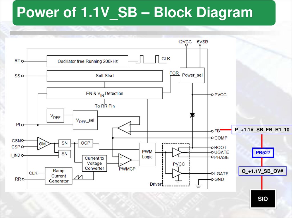
Power of VTTCPU – Block DiagramPower:
12V=>+VTTCPU
P_+VTTCPU_FB_R1_10
PR217
O_+VTTCPU_OV#
SIO
78.
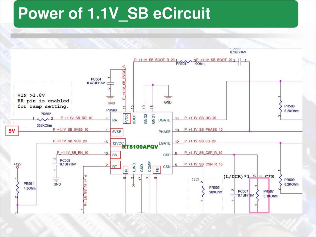
Power of 1.1V_SB eCircuit5V
79.
Power of 1.1V_SB – Block Diagram0
P_+1.1V_SB_FB_R1_10
PR527
O_+1.1V_SB_OV#
SIO
80.
P9X79 – AgendaIntel X79 Platform Structure
P9X79 Series Architecture
New Feature
Difference With P8 Series
Clock Distribution
Power Flow & Critical Power on X79 Platform
Power Sequence
Embedded Controller Introducing
SIO and Other Power Chipset Introducing
Power theory and working condition
Communication BUS Introducing
81.
DMIVCORE
VTTCPU
VSA_CPU
VCCPLL
1.5VDUAL_CD
1.5VDUAL_AB
3V
3VSB
1.1V_SB
1.5V_SB
1.1V_SB_VCCDMIPLL
C_PCH_DMI
C_PCH_DMI#
32.768 Hz
C_CPU
C_CPU#
C_CPU_QPI
C_CPU_QPI#
PCH
CPU
H_CPUPWRGD
H_CPURST#
O_PWROK
S_VRMPWRGD
S_PLTRST#
DMIRBIAS
DMI_ZCOMP
82.
DMIH_DMI_TXP[3:0]
H_DMI_TXN[3:0]
H_DMI_RXP[3:0]
CPU
PCH
H_DMI_RXN[3:0]
83.
SPI3V
3VSB
1.1V_SB
1.5V_SB
F1U1
3V_SPI (3VSB)
F1_SPI_HOLD#
O_BIOS_WP#
O2U6
5VSB
O2_SPI_SWITCH
(From EC)
C_PCH_14M
32.768 Hz
PCH
O_PWROK
S_VRMPWRGD
S_PLTRST#
84.
SPIO2_SPI_SWITCH
(From EC)
O2_SPI_MOSI_R
EC
O2_SPI_MISO_R
O2_SPI_CS1#_R
O2_SPI_MOSI_OUT
O2_SPI_CLK_R
O2U6
O2_SPI_MISO_OUT
O2_SPI_CS1#_OUT
F_SPI_MOSI
O2_SPI_CLK_OUT
F_SPI_MISO
F_SPI_CS1#
PCH
F_SPI_CLK
F1U1
85.
MEMORYVCORE
VTTCPU
VSA_CPU
VCCPLL
1.5VDUAL_CD
1.5VDUAL_AB
H_DRAMVREFDQ_TX_CD
H_DRAMVREFDQ_TX_AB
H_DRAMVREFDQ_RX_CD
H_DRAMVREFDQ_RX_AB
CPU
H_DDR_CD_1V05_SDA
H_DDR_AB_1V05_SDA
H_DDR_CD_1V05_SCL
H_DDR_AB_1V05_SCL
H_DRAMPWROK_CD
H_DRAMPWROK_AB
D3_MEMHOT#_AB
D3_MEMHOT#_CD
3V
1.5VDUAL_CD
1.5VDUAL_AB
+VTTDDR_AB
+VTTDDR_CD
D3_VREFDQ_A~D
D3_VREFCA_A~D
MEMORY
D3_M[A~D]_CLK[3:0]
D3_M[A~D]_CLK#[3:0]
D3_RESET#AB
D3_RESET#CD
H_DDR_CD_3V3_SDA
H_DDR_AB_3V3_SCL
H_DDR_CD_3V3_SDA
H_DDR_AB_3V3_SCL
86.
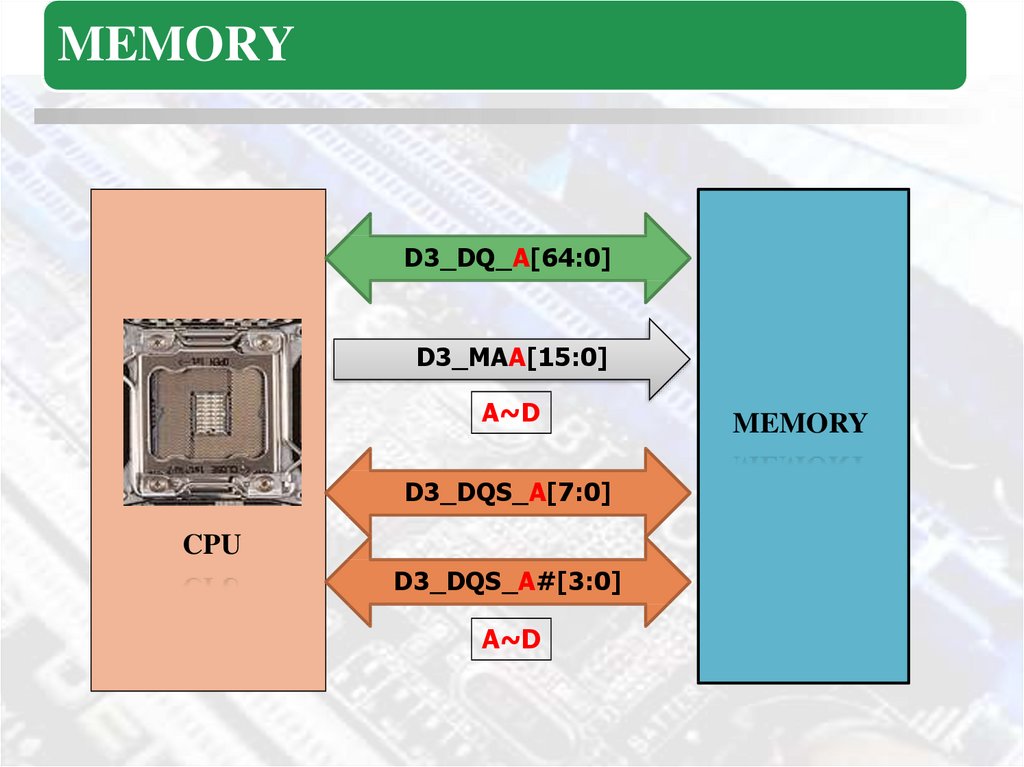
MEMORYD3_DQ_A[64:0]
D3_MAA[15:0]
A~D
D3_DQS_A[7:0]
CPU
D3_DQS_A#[3:0]
A~D
MEMORY
87.
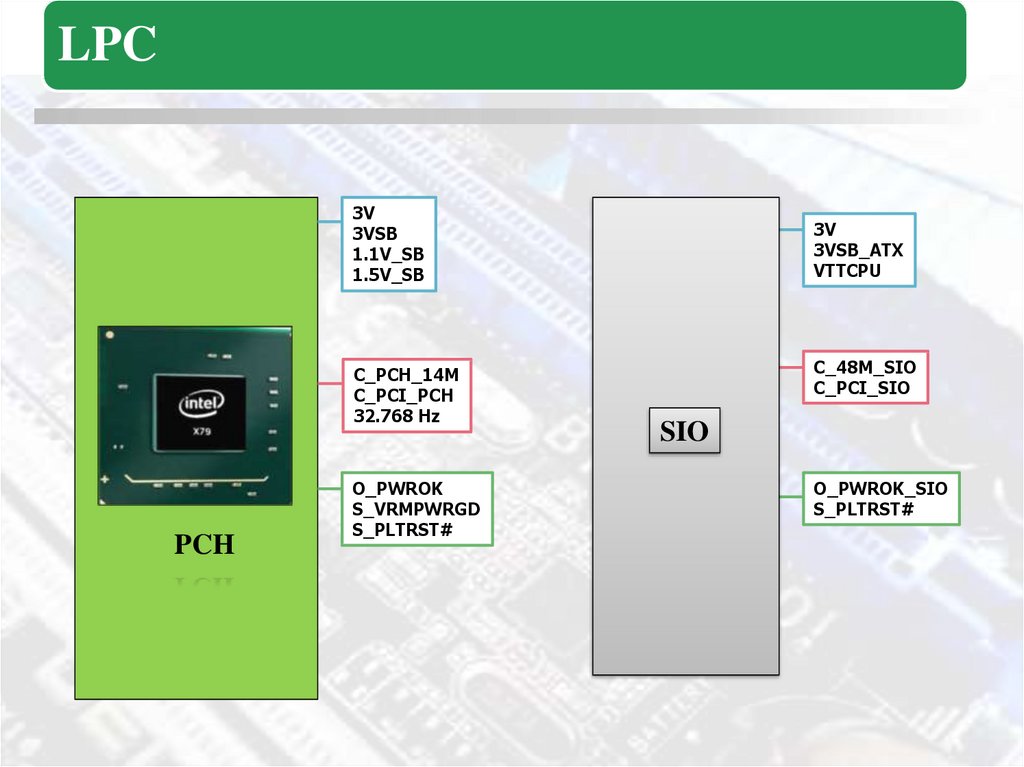
LPC3V
3VSB
1.1V_SB
1.5V_SB
C_PCH_14M
C_PCI_PCH
32.768 Hz
PCH
O_PWROK
S_VRMPWRGD
S_PLTRST#
3V
3VSB_ATX
VTTCPU
C_48M_SIO
C_PCI_SIO
SIO
SIO
O_PWROK_SIO
S_PLTRST#
88.
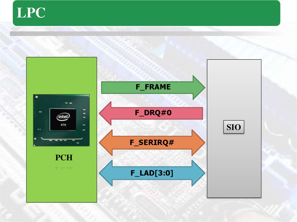
LPCF_FRAME
F_DRQ#0
SIO
F_SERIRQ#
PCH
F_LAD[3:0]
89.
P9X79 Series – Q&A~Q &A~
~THANK YOU~