


 Электроника
Похожие презентации:
")


")

![PBA Repair Guide [GT-S8000]](https://cf.ppt-online.org/files/thumb/t/tIHBnfpml5G6E47aLocdVU0kDZQNvuejRhAMC8.jpg "PBA Repair Guide [GT-S8000]")


 Wireless Audio - Soundbar ’2017 SAMSUNG ELECTRONICS CO.,LTD. VD R&D GROUP")
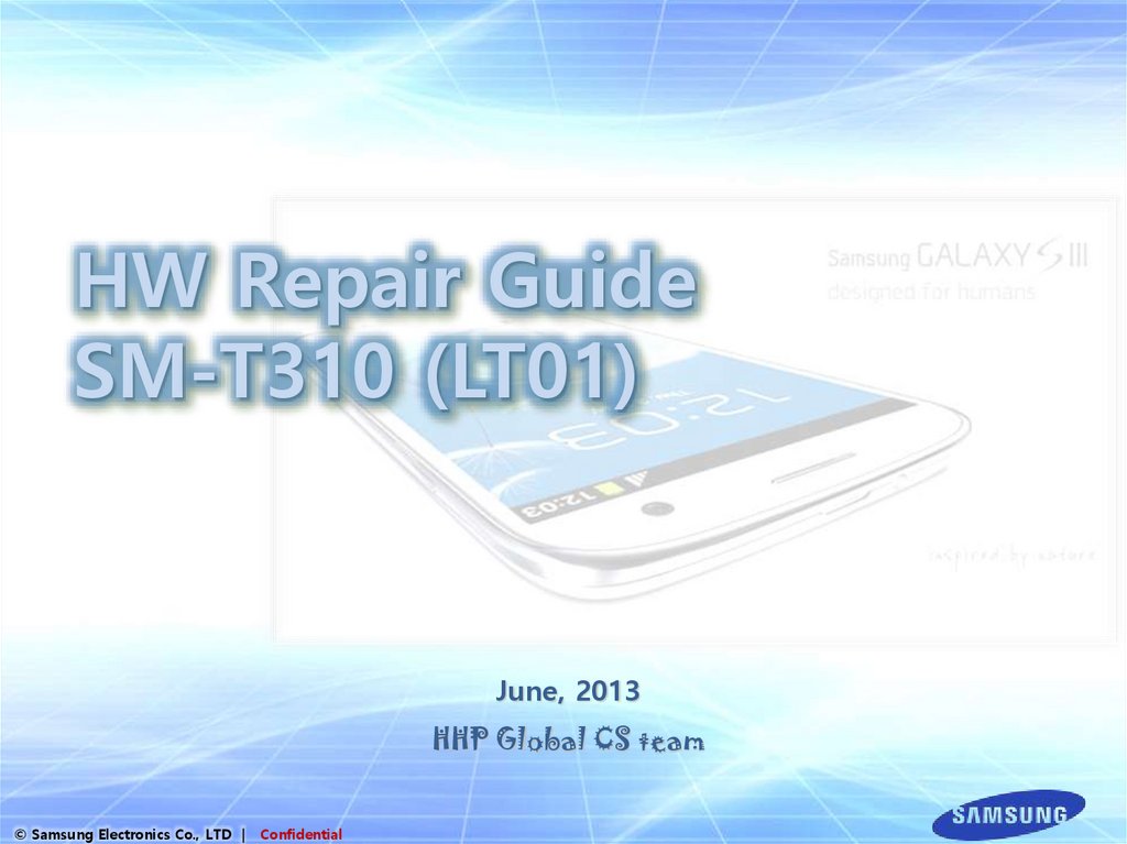
HW Repair Guide SM-T310 (LT01)
1.
HW Repair GuideSM-T310 (LT01)
June, 2013
HHP Global CS team
© Samsung Electronics Co., LTD |
Confidential
2.
NOTICE1. All functionality, features, specifications and other product
information provided in this document including, but not limited
to, the benefits, design, pricing, components, performance,
availability, and capabilities of the product are subject to change
without notice or obligation. Samsung reserves the right to make changes to this docume
nt and the product described herein, at anytime, without obligation on Samsung to provid
e notification of such change.
2. In data of our company, important management / technical information is included,
and if it is leaked, loss can happen in various aspect such as closing a technology gap,
increasing ability to respond.
Therefore, it is strictly prohibited from information leak or forwarding this material, and if
leak of management / technical information due to disobeying the law happens, it can be
severely punished in accordance with information protection rule of our company.
© Samsung Electronics Co., LTD |
Confidential
2
3.
Contents1.
Introduction of LT01
2.
Service Guide
Boot Recovery
3.
Repair Guide
4.
Assembly & Disassembly
Electronic Components
SMD parts
Trouble Shooting
Q&A
© Samsung Electronics Co., LTD |
Confidential
3
4.
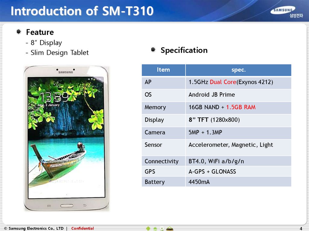
Introduction of SM-T310Feature
- 8” Display
- Slim Design Tablet
Specification
Item
© Samsung Electronics Co., LTD |
Confidential
spec.
AP
1.5GHz Dual Core(Exynos 4212)
OS
Android JB Prime
Memory
16GB NAND + 1.5GB RAM
Display
8” TFT (1280x800)
Camera
5MP + 1.3MP
Sensor
Accelerometer, Magnetic, Light
Connectivity
BT4.0, WiFi a/b/g/n
GPS
A-GPS + GLONASS
Battery
4450mA
4
5.
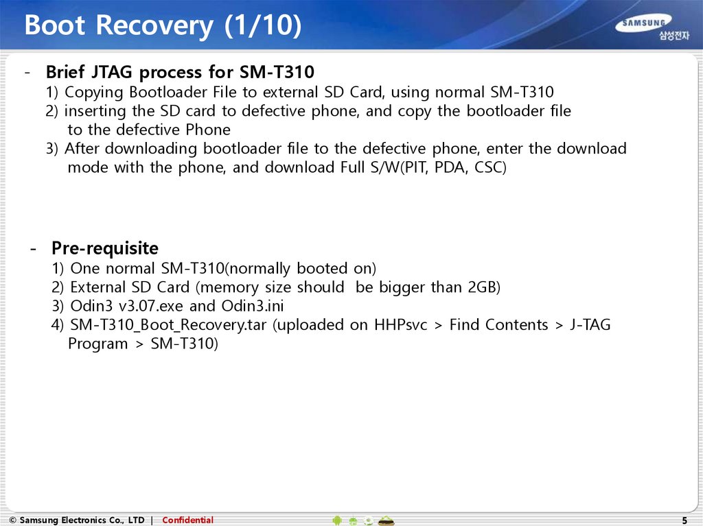
Boot Recovery (1/10)- Brief JTAG process for SM-T310
1) Copying Bootloader File to external SD Card, using normal SM-T310
2) inserting the SD card to defective phone, and copy the bootloader file
to the defective Phone
3) After downloading bootloader file to the defective phone, enter the download
mode with the phone, and download Full S/W(PIT, PDA, CSC)
- Pre-requisite
1)
2)
3)
4)
One normal SM-T310(normally booted on)
External SD Card (memory size should be bigger than 2GB)
Odin3 v3.07.exe and Odin3.ini
SM-T310_Boot_Recovery.tar (uploaded on HHPsvc > Find Contents > J-TAG
Program > SM-T310)
© Samsung Electronics Co., LTD |
Confidential
5
6.
Boot Recovery (2/10)© Samsung Electronics Co., LTD |
Confidential
6
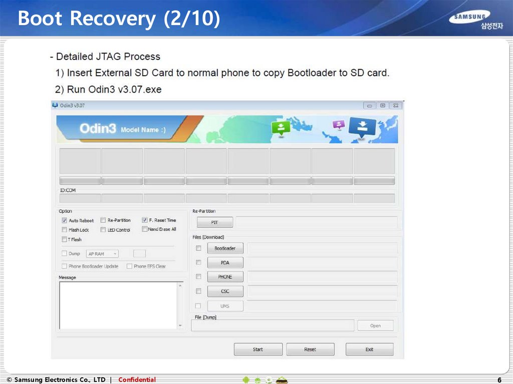
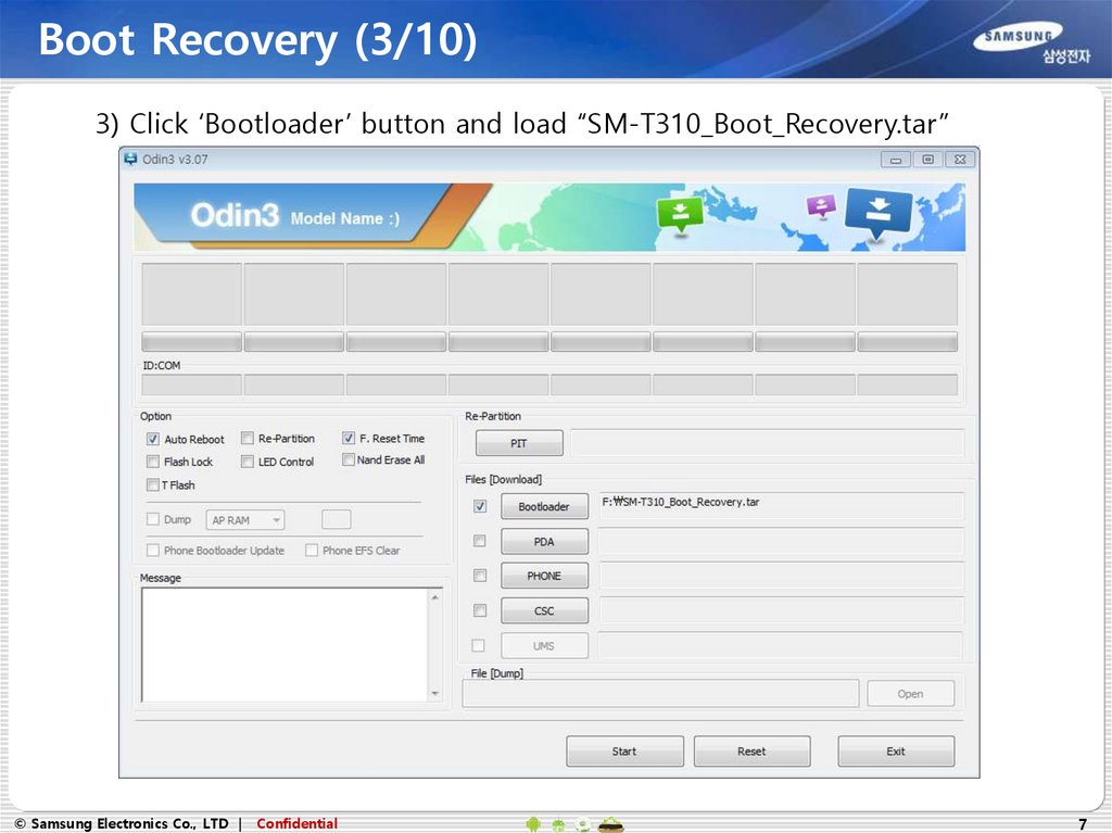
7.
Boot Recovery (3/10)3) Click ‘Bootloader’ button and load “SM-T310_Boot_Recovery.tar”
© Samsung Electronics Co., LTD |
Confidential
7
8.
Boot Recovery (4/10)4) Enter download mode with the normal phone(SD Card inserted).
※ Download Mode : Volume Down Key + Power Key and press Volume Up key.
<Volume Down key + Power Key>
© Samsung Electronics Co., LTD |
Confidential
<Download Mode>
8
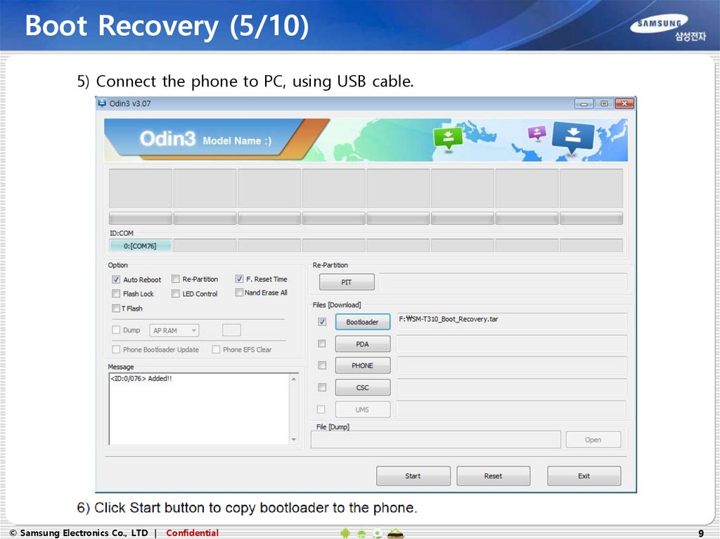
9.
Boot Recovery (5/10)5) Connect the phone to PC, using USB cable.
© Samsung Electronics Co., LTD |
Confidential
9
10.
Boot Recovery (6/10)7) Disconnect the phone from PC.
8) Close the Odin3 v3.07.exe and Run it again.
9) Click ‘Bootloader’ button and load “SM-T310_Boot_Recovery.tar”
And check ‘T Flash’ option in the Odin, to copy bootloader to SD Card
© Samsung Electronics Co., LTD |
Confidential
10
11.
Boot Recovery (7/10)10) Enter download mode with the normal phone(bootloader was copied before),
and connect it to PC again
11) Click Start button to copy bootloader to the SD Card
© Samsung Electronics Co., LTD |
Confidential
11
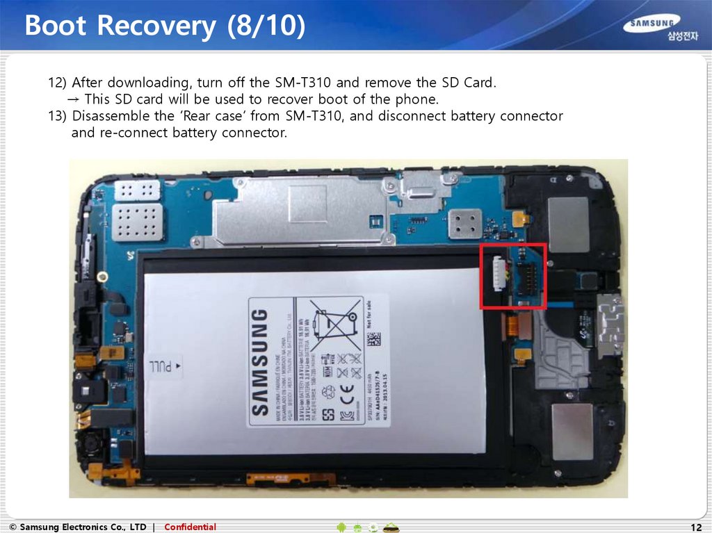
12.
Boot Recovery (8/10)12) After downloading, turn off the SM-T310 and remove the SD Card.
→ This SD card will be used to recover boot of the phone.
13) Disassemble the ‘Rear case’ from SM-T310, and disconnect battery connector
and re-connect battery connector.
© Samsung Electronics Co., LTD |
Confidential
12
13.
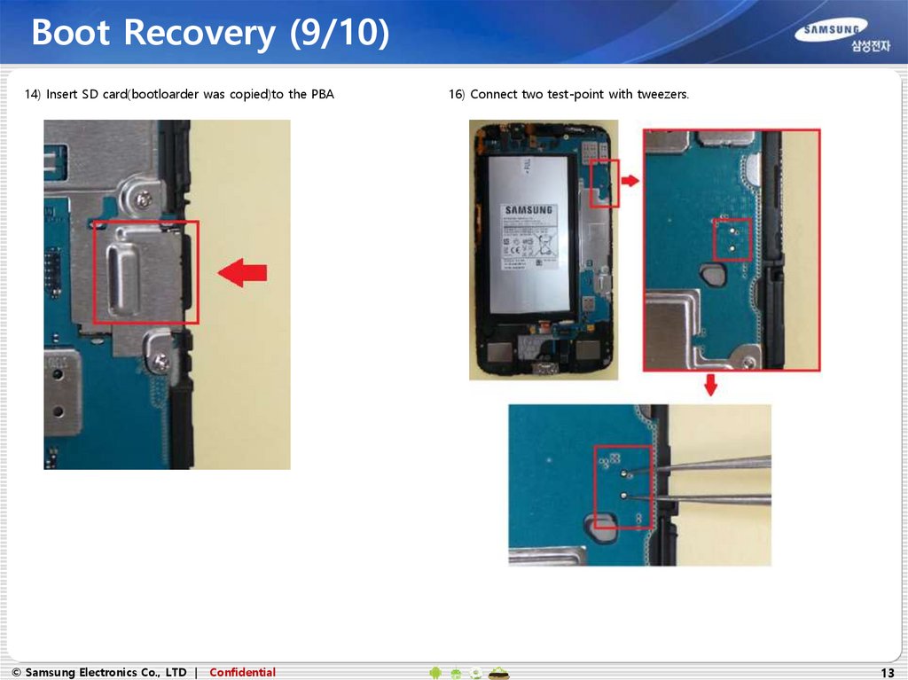
Boot Recovery (9/10)14) Insert SD card(bootloarder was copied)to the PBA
© Samsung Electronics Co., LTD |
Confidential
16) Connect two test-point with tweezers.
13
14.
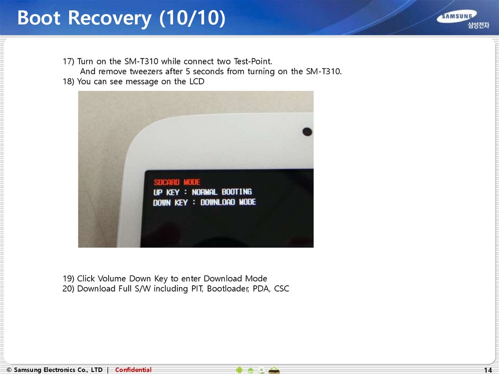
Boot Recovery (10/10)17) Turn on the SM-T310 while connect two Test-Point.
And remove tweezers after 5 seconds from turning on the SM-T310.
18) You can see message on the LCD
19) Click Volume Down Key to enter Download Mode
20) Download Full S/W including PIT, Bootloader, PDA, CSC
© Samsung Electronics Co., LTD |
Confidential
14
15.
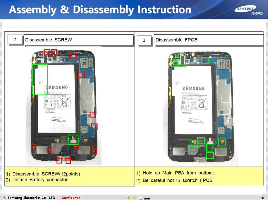
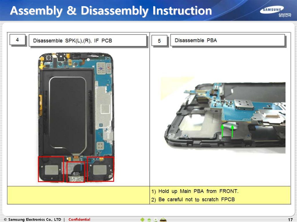
Assembly & Disassembly Instruction1. Disassembly
© Samsung Electronics Co., LTD |
Confidential
15
16.
Assembly & Disassembly Instruction© Samsung Electronics Co., LTD |
Confidential
16
17.
Assembly & Disassembly Instruction© Samsung Electronics Co., LTD |
Confidential
17
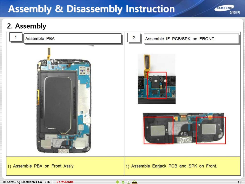
18.
Assembly & Disassembly Instruction2. Assembly
© Samsung Electronics Co., LTD |
Confidential
18
19.
Assembly & Disassembly Instruction© Samsung Electronics Co., LTD |
Confidential
19
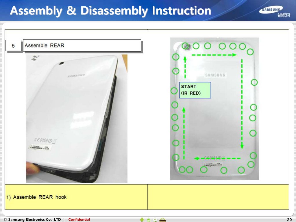
20.
Assembly & Disassembly Instruction© Samsung Electronics Co., LTD |
Confidential
20
21.
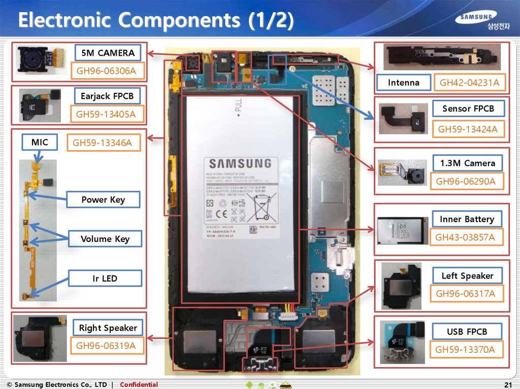
Electronic Components (1/2)5M CAMERA
GH96-06306A
Intenna
GH42-04231A
Earjack FPCB
GH59-13405A
Sensor FPCB
GH59-13424A
MIC
GH59-13346A
1.3M Camera
GH96-06290A
Power Key
Inner Battery
Volume Key
GH43-03857A
Ir LED
Left Speaker
GH96-06317A
Right Speaker
USB FPCB
GH96-06319A
GH59-13370A
© Samsung Electronics Co., LTD |
Confidential
21
22.
Electronic Components (2/2)TSP Connector
LCD TSP Assy
GH96-06467A
LCD Connector
Home Key FPCB
© Samsung Electronics Co., LTD |
Confidential
GH59-13343A
22
23.
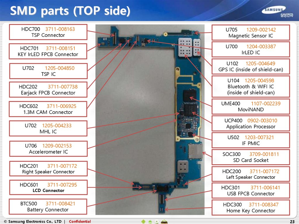
SMD parts (TOP side)HDC700 3711-008163
TSP Connector
HDC701 3711-008151
KEY IrLED FPCB Connector
U702
1205-004850
TSP IC
HDC202
3711-007738
Earjack FPCB Connector
HDC602
3711-006925
1.3M CAM Connector
U702
1205-004233
MHL IC
U706 1209-002153
Accelerometer IC
HDC201
3711-007172
Right Speaker Connector
HDC601
3711-007295
U705
1209-002142
Magnetic Sensor IC
U700
1204-003387
IrLED IC
U102 1205-004649
GPS IC (inside of shield-can)
U104 1205-004598
Bluetooth & WIFI IC
(inside of shield-can)
UME400
1107-002239
MoviNAND
UCP400 0902-003010
Application Processor
U502
1203-007321
IF PMIC
SOC300
3709-001811
SD Card Socket
HDC200
3711-007172
Left Speaker Connector
LCD Connector
HDC301
3711-006141
USB FPCB Connector
BTC500
3711-008421
Battery Connector
HDC300 3711-008347
Home Key Connector
© Samsung Electronics Co., LTD |
Confidential
23
24.
SMD parts (Bottom side)HDC600 3708-002222
5M Camera Connector
F600 2901-001625
F602 2901-001732
Filter for 5M Camera
ANT100, ANT101
3712-001473
Antenna Contact (BT, Wifi, GPS)
U204 1205-004804
Audio Codec
F601 2901-001625
F603, F604 2901-001732
Filter for LCD
© Samsung Electronics Co., LTD |
Confidential
24
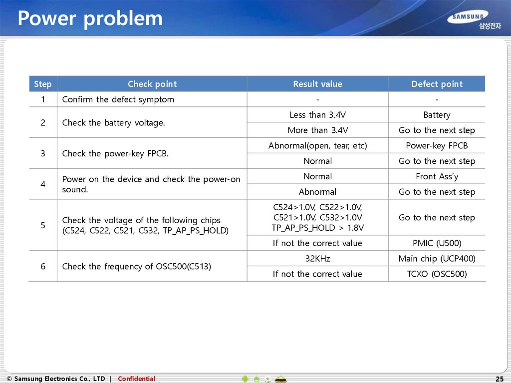
25.
Power problemStep
Check point
1
Confirm the defect symptom
2
Check the battery voltage.
3
Check the power-key FPCB.
4
Power on the device and check the power-on
sound.
5
6
Check the voltage of the following chips
(C524, C522, C521, C532, TP_AP_PS_HOLD)
Check the frequency of OSC500(C513)
© Samsung Electronics Co., LTD |
Confidential
Result value
Defect point
-
-
Less than 3.4V
Battery
More than 3.4V
Go to the next step
Abnormal(open, tear, etc)
Power-key FPCB
Normal
Go to the next step
Normal
Front Ass’y
Abnormal
Go to the next step
C524>1.0V, C522>1.0V,
C521>1.0V, C532>1.0V
TP_AP_PS_HOLD > 1.8V
Go to the next step
If not the correct value
PMIC (U500)
32KHz
Main chip (UCP400)
If not the correct value
TCXO (OSC500)
25
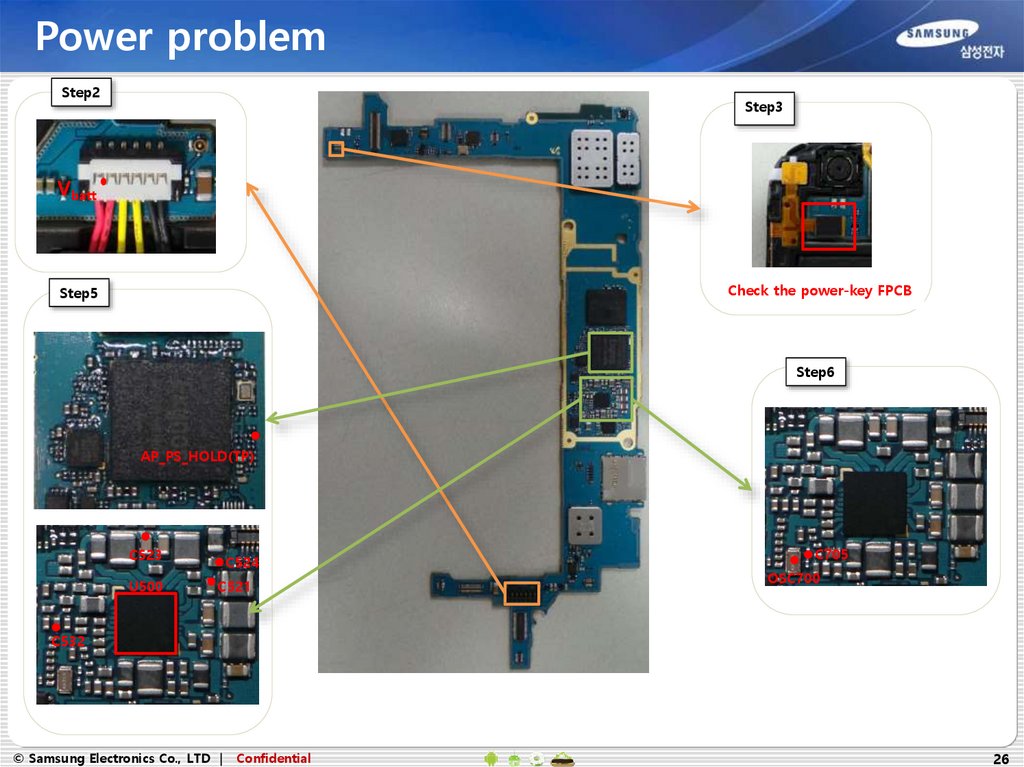
26.
Power problemStep2
Step3
Vbatt
Check the power-key FPCB
Step5
Step6
AP_PS_HOLD(TP)
C523
U500
C524
C521
C705
OSC700
C532
© Samsung Electronics Co., LTD |
Confidential
26
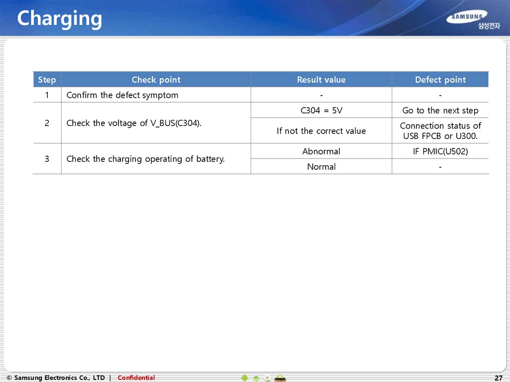
27.
ChargingStep
1
Check point
Confirm the defect symptom
2
Check the voltage of V_BUS(C304).
3
Check the charging operating of battery.
© Samsung Electronics Co., LTD |
Confidential
Result value
Defect point
-
-
C304 = 5V
Go to the next step
If not the correct value
Connection status of
USB FPCB or U300.
Abnormal
IF PMIC(U502)
Normal
-
27
28.
ChargingStep2, 3
U502
C304
© Samsung Electronics Co., LTD |
Confidential
28
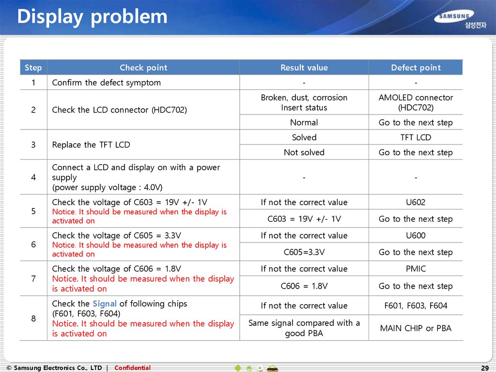
29.
Display problemStep
1
2
Check point
Confirm the defect symptom
Check the LCD connector (HDC702)
3
Replace the TFT LCD
4
Connect a LCD and display on with a power
supply
(power supply voltage : 4.0V)
5
6
Check the voltage of C603 = 19V +/- 1V
Notice. It should be measured when the display is
activated on
Check the voltage of C605 = 3.3V
Notice. It should be measured when the display is
activated on
Result value
Defect point
-
-
Broken, dust, corrosion
Insert status
AMOLED connector
(HDC702)
Normal
Go to the next step
Solved
TFT LCD
Not solved
Go to the next step
-
-
If not the correct value
U602
C603 = 19V +/- 1V
Go to the next step
If not the correct value
U600
C605=3.3V
Go to the next step
7
Check the voltage of C606 = 1.8V
Notice. It should be measured when the display
is activated on
If not the correct value
PMIC
C606 = 1.8V
Go to the next step
If not the correct value
F601, F603, F604
8
Check the Signal of following chips
(F601, F603, F604)
Notice. It should be measured when the display
is activated on
Same signal compared with a
good PBA
MAIN CHIP or PBA
© Samsung Electronics Co., LTD |
Confidential
29
30.
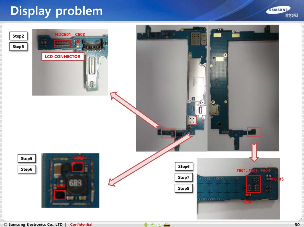
Display problemStep2
HDC601 C603
Step5
LCD CONNECTOR
U602
Step5
Step6
Step6
F601, F603, F604
Step7
U600
C605
Step8
C606
© Samsung Electronics Co., LTD |
Confidential
30
31.
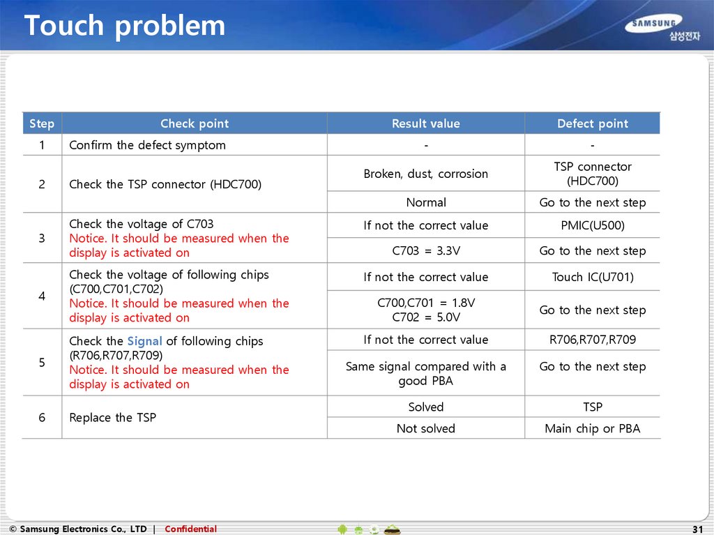
Touch problemStep
Result value
Defect point
-
-
Broken, dust, corrosion
TSP connector
(HDC700)
Normal
Go to the next step
3
Check the voltage of C703
Notice. It should be measured when the
display is activated on
If not the correct value
PMIC(U500)
C703 = 3.3V
Go to the next step
If not the correct value
Touch IC(U701)
4
Check the voltage of following chips
(C700,C701,C702)
Notice. It should be measured when the
display is activated on
C700,C701 = 1.8V
C702 = 5.0V
Go to the next step
If not the correct value
R706,R707,R709
5
Check the Signal of following chips
(R706,R707,R709)
Notice. It should be measured when the
display is activated on
Same signal compared with a
good PBA
Go to the next step
6
Replace the TSP
Solved
TSP
Not solved
Main chip or PBA
1
2
Check point
Confirm the defect symptom
Check the TSP connector (HDC700)
© Samsung Electronics Co., LTD |
Confidential
31
32.
TSP problemStep2
HDC700
Step3 ~ 4
TSP power
C701
C703
C700
C702
R909
R907
R906
Step5
TSP CONNECTOR
© Samsung Electronics Co., LTD |
Confidential
TSP signal
32
33.
5M CAM ProblemStep
1
2
3
4
Check point
Confirm the defect symptom
Check the 5M CAM connector (HDC900)
Check the voltage of following chips
(C601, C602, C621)
Notice. It should be measured when the 5M
CAM is activated on
Check the clock of C600
Notice. It should be measured when the 5M
CAM is activated on
5
Check the F600, F602
Notice. It should be measured when the 5M
CAM is activated on
6
Replace the 5M CAM
© Samsung Electronics Co., LTD |
Confidential
Result value
Defect point
-
-
Broken, dust, corrosion
5M CAM connector
(HDC600)
Normal
Go to the next step
If not the correct value
C601, C602,
C629, C630
C601 = 1.2V, C602 = 1.8V,
C621 = 2.8V
Go to the next step
C600 = 12Mhz
(Same signal compared with a
good PBA)
Go to the next step
If not the correct value
Main chip
Abnormal
F600, F602
Normal
Go to the next step
Solved
5M CAM
Not solved
Main chip or PBA
33
34.
5M CAM ProblemHDC600
C600
F602
F600
C601
C602
C621
© Samsung Electronics Co., LTD |
Confidential
34
35.
1.3M CAM ProblemStep
1
2
Check point
Confirm the defect symptom
Check the 1.3M CAM connector (HDC602)
3
Check the voltage of following chips
(C612, C613, C614)
Notice. It should be measured when the
1.3M CAM is activated on
4
Check the clock of C609
Notice. It should be measured when the
1.3M CAM is activated on
5
Check the F605
Notice. It should be measured when the
1.3M CAM is activated on
6
Replace the 1.3M CAM
© Samsung Electronics Co., LTD |
Confidential
Result value
Defect point
-
-
Broken, dust, corrosion
1.3M CAM connector
(HDC602)
Normal
Go to the next step
If not the correct value
C612, C613, C614
C612 = 1.8V, C613 = 1.8V,
C614 = 2.8V
Go to the next step
C609 = 24Mhz
(Same signal compared with a
good PBA)
Go to the next step
If not the correct value
Main chip
Abnormal
F902
Normal
Go to the next step
Solved
1.3M CAM
Not solved
Main chip or PBA
35
36.
1.3M CAM ProblemC612
HDC602
C613
C609
F605
C614
© Samsung Electronics Co., LTD |
Confidential
36
37.
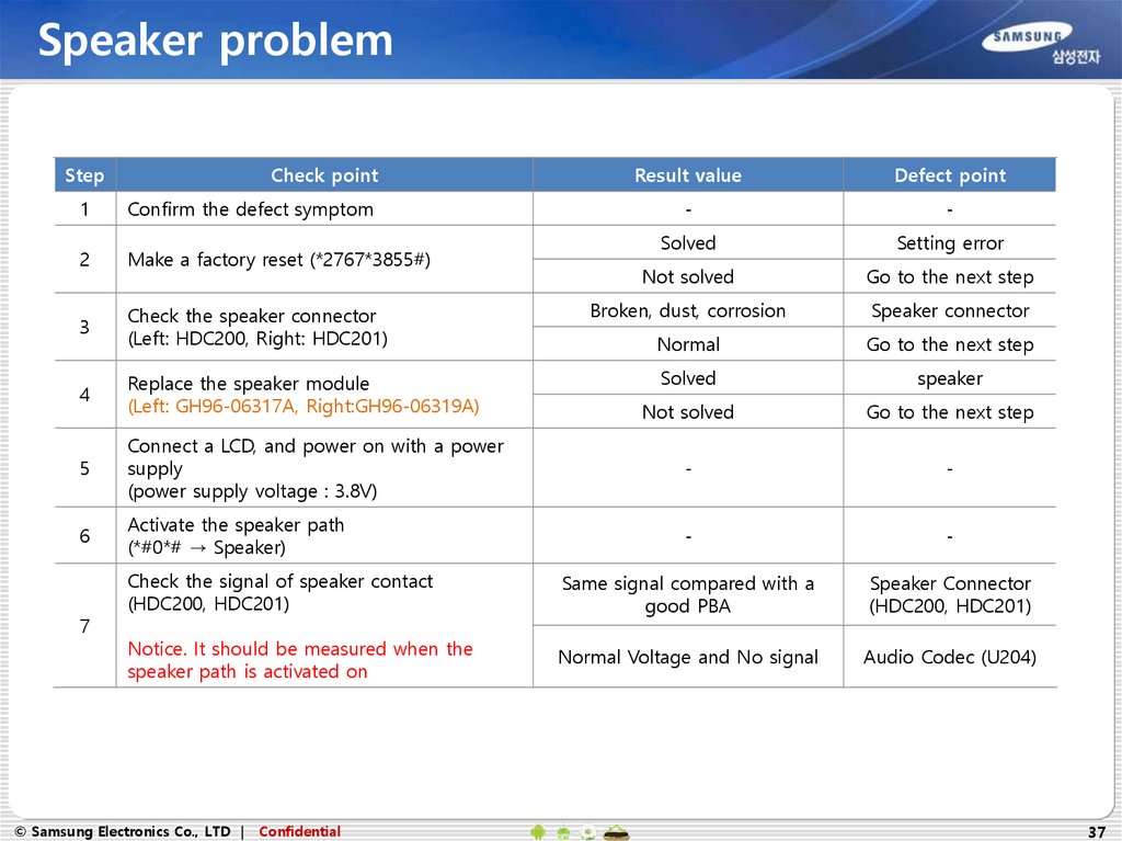
Speaker problemStep
Check point
Result value
Defect point
-
-
Solved
Setting error
Not solved
Go to the next step
Broken, dust, corrosion
Speaker connector
Normal
Go to the next step
Solved
speaker
Not solved
Go to the next step
1
Confirm the defect symptom
2
Make a factory reset (*2767*3855#)
3
Check the speaker connector
(Left: HDC200, Right: HDC201)
4
Replace the speaker module
(Left: GH96-06317A, Right:GH96-06319A)
5
Connect a LCD, and power on with a power
supply
(power supply voltage : 3.8V)
-
-
6
Activate the speaker path
(*#0*# → Speaker)
-
-
Check the signal of speaker contact
(HDC200, HDC201)
Same signal compared with a
good PBA
Speaker Connector
(HDC200, HDC201)
Notice. It should be measured when the
speaker path is activated on
Normal Voltage and No signal
Audio Codec (U204)
7
© Samsung Electronics Co., LTD |
Confidential
37
38.
Speaker problemStep3
Step4
Right Speaker Module
(GH96-06319A)
Left Speaker Module
(GH96-06317A)
HDC200, HDC201
Speaker connector
Step7
HDC201
HDC200
Sound signal path
U204
Audio Codec
© Samsung Electronics Co., LTD |
Confidential
38
39.
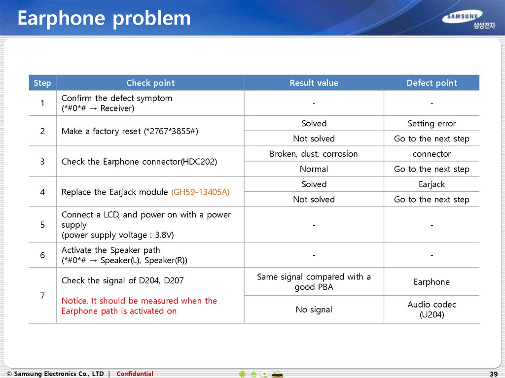
Earphone problemStep
Check point
Result value
Defect point
-
-
Solved
Setting error
Not solved
Go to the next step
Broken, dust, corrosion
connector
Normal
Go to the next step
Solved
Earjack
Not solved
Go to the next step
1
Confirm the defect symptom
(*#0*# → Receiver)
2
Make a factory reset (*2767*3855#)
3
Check the Earphone connector(HDC202)
4
Replace the Earjack module (GH59-13405A)
5
Connect a LCD, and power on with a power
supply
(power supply voltage : 3.8V)
-
-
6
Activate the Speaker path
(*#0*# → Speaker(L), Speaker(R))
-
-
Check the signal of D204, D207
Same signal compared with a
good PBA
Earphone
No signal
Audio codec
(U204)
7
Notice. It should be measured when the
Earphone path is activated on
© Samsung Electronics Co., LTD |
Confidential
39
40.
Earphone problemStep3
Step4
Earjack
(GH59-13405A)
Earjack connector
Step7
D204
D207
© Samsung Electronics Co., LTD |
Confidential
40
41.
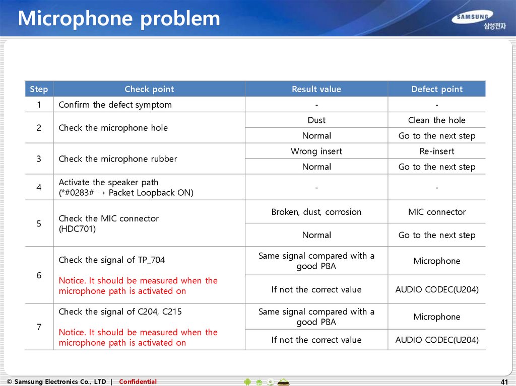
Microphone problemStep
Check point
1
Confirm the defect symptom
2
Check the microphone hole
3
Check the microphone rubber
4
Activate the speaker path
(*#0283# → Packet Loopback ON)
5
Check the MIC connector
(HDC701)
Check the signal of TP_704
6
Notice. It should be measured when the
microphone path is activated on
Check the signal of C204, C215
7
Notice. It should be measured when the
microphone path is activated on
© Samsung Electronics Co., LTD |
Confidential
Result value
Defect point
-
-
Dust
Clean the hole
Normal
Go to the next step
Wrong insert
Re-insert
Normal
Go to the next step
-
-
Broken, dust, corrosion
MIC connector
Normal
Go to the next step
Same signal compared with a
good PBA
Microphone
If not the correct value
AUDIO CODEC(U204)
Same signal compared with a
good PBA
Microphone
If not the correct value
AUDIO CODEC(U204)
41
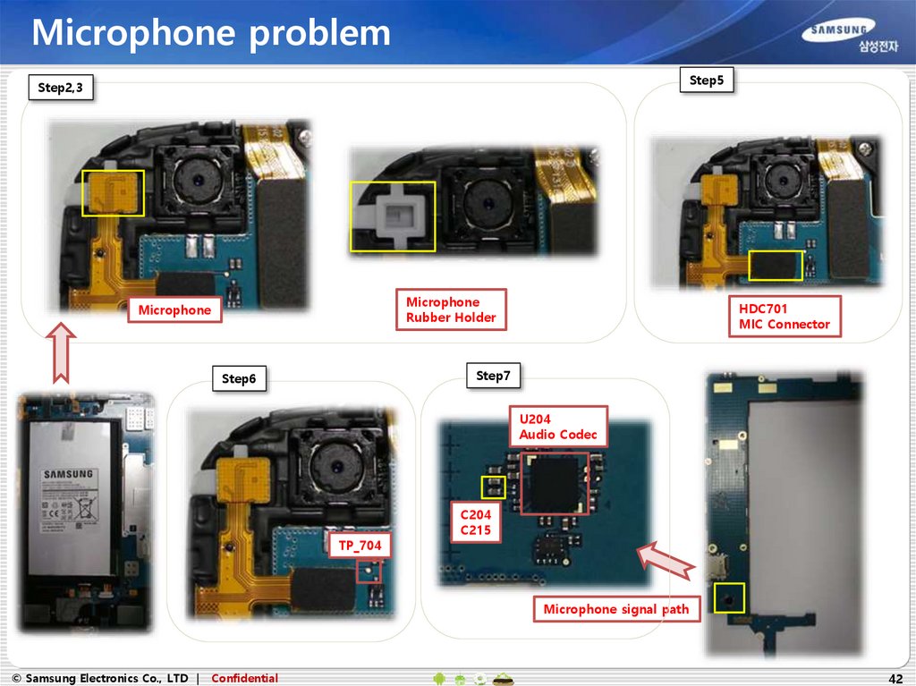
42.
Microphone problemStep5
Step2,3
Microphone
Rubber Holder
Microphone
HDC701
MIC Connector
Step7
Step6
U204
Audio Codec
TP_704
C204
C215
Microphone signal path
© Samsung Electronics Co., LTD |
Confidential
42
43.
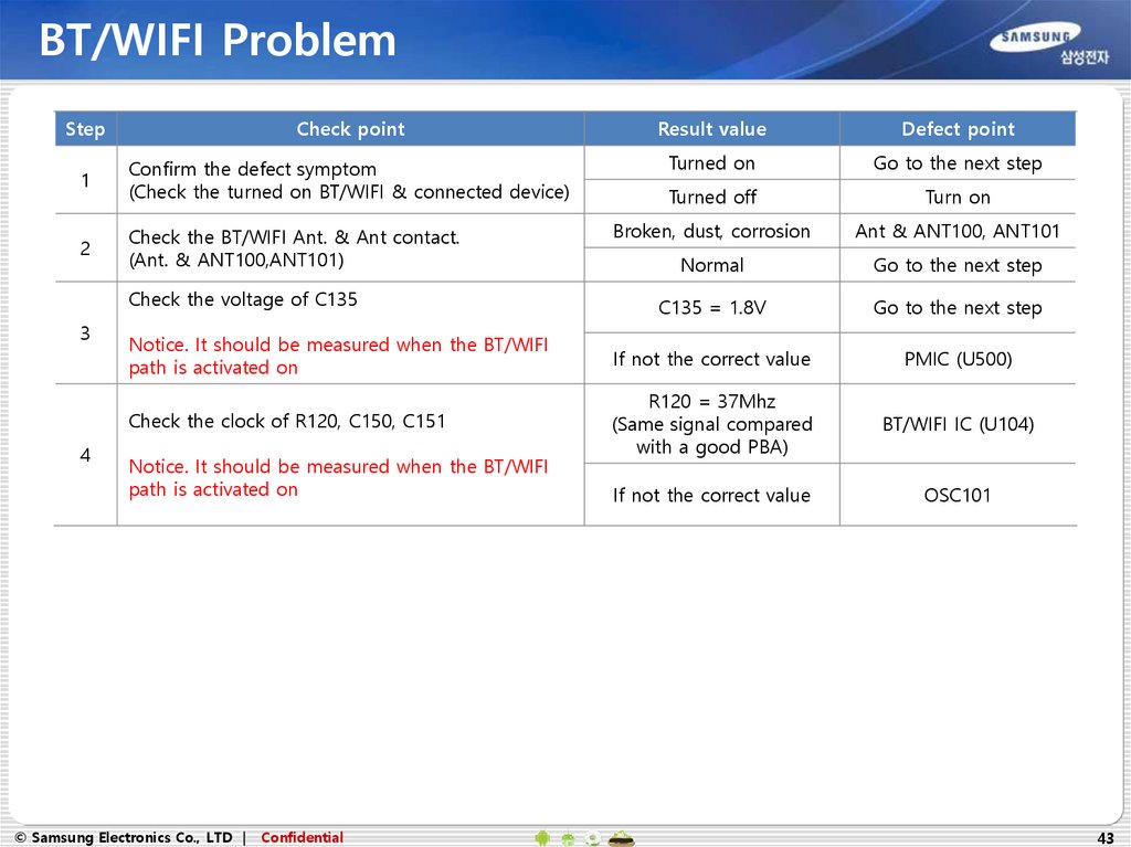
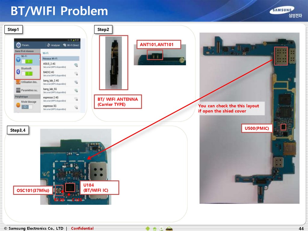
BT/WIFI ProblemStep
Check point
Result value
Defect point
1
Confirm the defect symptom
(Check the turned on BT/WIFI & connected device)
Turned on
Go to the next step
Turned off
Turn on
2
Check the BT/WIFI Ant. & Ant contact.
(Ant. & ANT100,ANT101)
Broken, dust, corrosion
Ant & ANT100, ANT101
Normal
Go to the next step
C135 = 1.8V
Go to the next step
Notice. It should be measured when the BT/WIFI
path is activated on
If not the correct value
PMIC (U500)
Check the clock of R120, C150, C151
R120 = 37Mhz
(Same signal compared
with a good PBA)
BT/WIFI IC (U104)
If not the correct value
OSC101
Check the voltage of C135
3
4
Notice. It should be measured when the BT/WIFI
path is activated on
© Samsung Electronics Co., LTD |
Confidential
43
44.
BT/WIFI ProblemStep1
Step2
ANT101,ANT101
BT/ WIFI ANTENNA
(Carrier TYPE)
You can check the this layout
if open the shied cover
U500(PMIC)
Step3,4
U104
(BT/WIFI IC)
OSC101(37Mhz)
R120
© Samsung Electronics Co., LTD |
C135
Confidential
44
45.
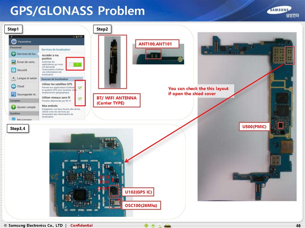
GPS/GLONASS ProblemStep
Check point
Result value
Defect point
Turned on
Go to the next step
Turned off
Turn on
1
Confirm the defect symptom
(Check the turned on GPS function)
2
Check the BT/WIFI Ant. & Ant contact.
(Ant. & ANT100, ANT101)
Broken, dust, corrosion
BT/WIFI Ant &
ANT100, ANT101
Normal
Go to the next step
Check the voltage of C110, C113, L101
C110 = 1.8V
C113, L101 = 2.8V
Go to the next step
Notice. It should be measured when the GPS path
is activated on
If not the correct value
PMIC(U500)
Check the clock of OSC100
OSC100 = 26Mhz
(Same signal compared
with a good PBA)
GPS IC(U102)
GPS LNA(U101)
If not the correct value
OSC100
3
4
Notice. It should be measured when the GPS path
is activated on
© Samsung Electronics Co., LTD |
Confidential
45
46.
GPS/GLONASS ProblemStep1
Step2
ANT100,ANT101
BT/ WIFI ANTENNA
(Carrier TYPE)
You can check the this layout
if open the shied cover
U500(PMIC)
Step3,4
C113
L101
C110
U102(GPS IC)
OSC100(26Mhz)
© Samsung Electronics Co., LTD |
Confidential
46
47.
Q&AQuestion
© Samsung Electronics Co., LTD |
Confidential
47