

 Электроника
Похожие презентации:
 An introduction")


")


Mems its methods and applications
1.
MEMSits methods and applications
CHE 384T – Graduate Student Presentation
11/14/17
Ji Yeon Kim
The Department of Chemical Engineering
The University of Texas at Austin
2.
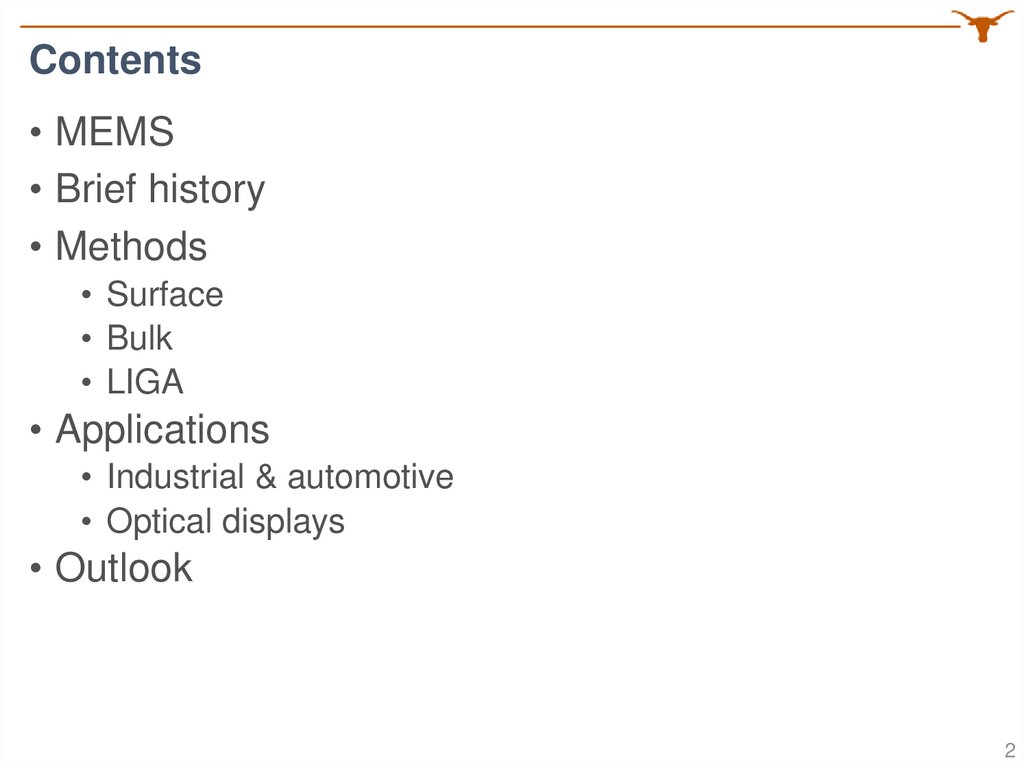
Contents• MEMS
• Brief history
• Methods
• Surface
• Bulk
• LIGA
• Applications
• Industrial & automotive
• Optical displays
• Outlook
2
3.
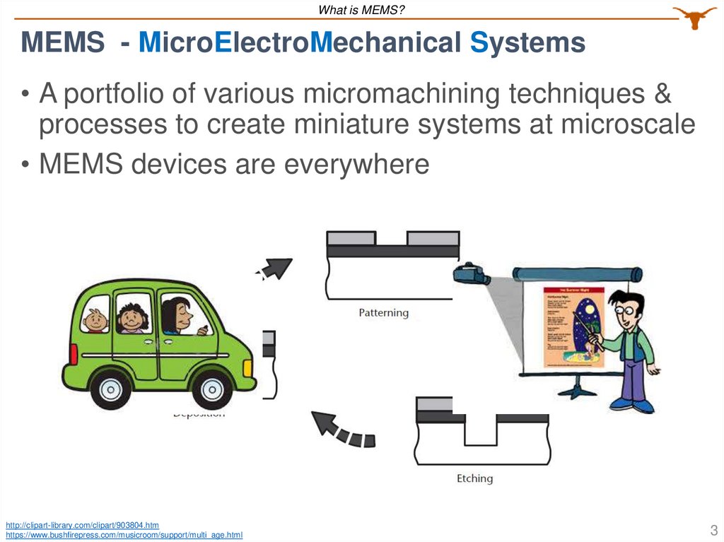
What is MEMS?MEMS - MicroElectroMechanical Systems
• A portfolio of various micromachining techniques &
processes to create miniature systems at microscale
• MEMS devices are everywhere
http://clipart-library.com/clipart/903804.htm
https://www.bushfirepress.com/musicroom/support/multi_age.html
3
4.
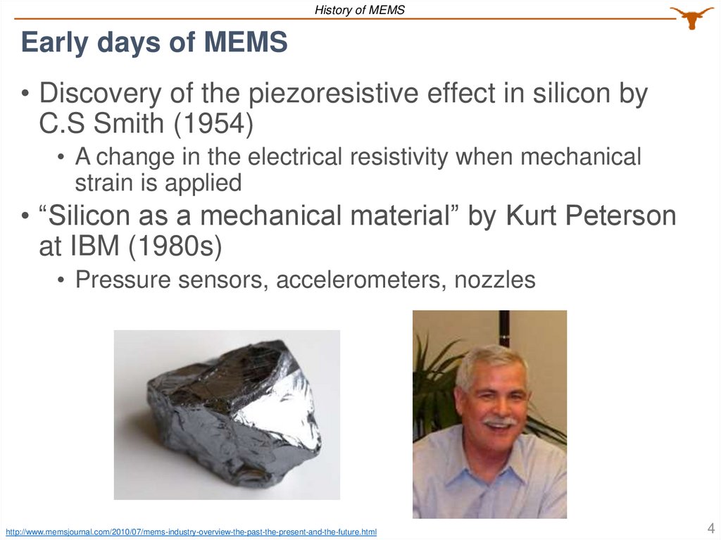
History of MEMSEarly days of MEMS
• Discovery of the piezoresistive effect in silicon by
C.S Smith (1954)
• A change in the electrical resistivity when mechanical
strain is applied
• “Silicon as a mechanical material” by Kurt Peterson
at IBM (1980s)
• Pressure sensors, accelerometers, nozzles
http://www.memsjournal.com/2010/07/mems-industry-overview-the-past-the-present-and-the-future.html
4
5.
Various methods of MEMS• Surface micromachining
• Bulk micromachining
• LIGA
5
6.
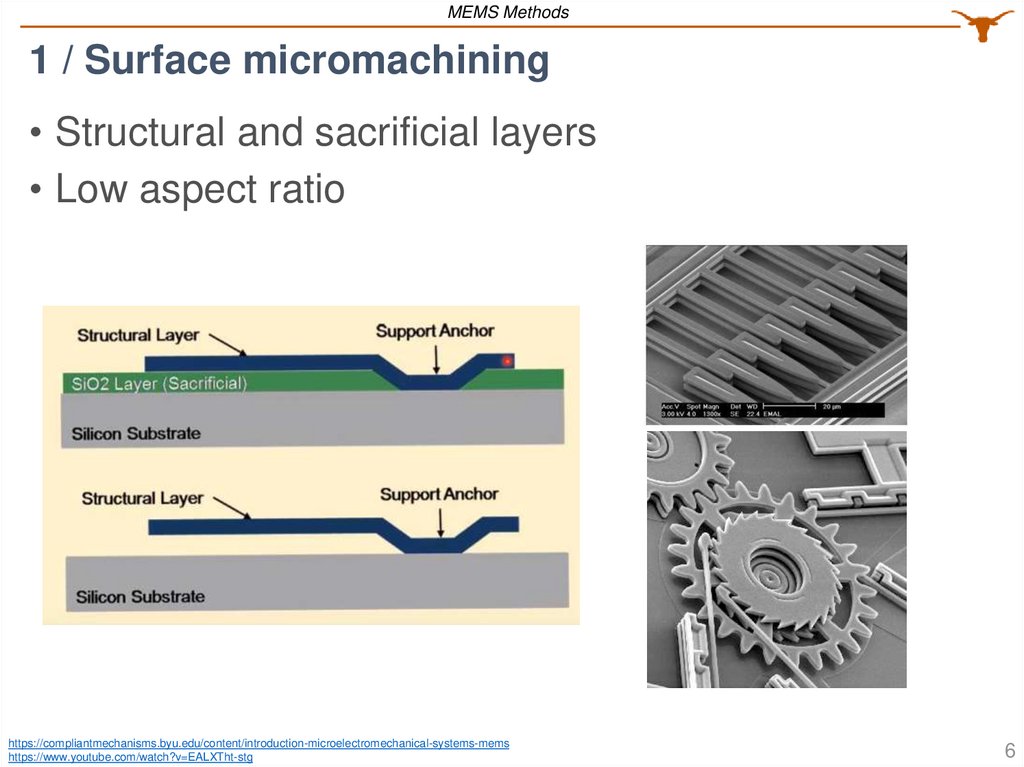
MEMS Methods1 / Surface micromachining
• Structural and sacrificial layers
• Low aspect ratio
https://compliantmechanisms.byu.edu/content/introduction-microelectromechanical-systems-mems
https://www.youtube.com/watch?v=EALXTht-stg
6
7.
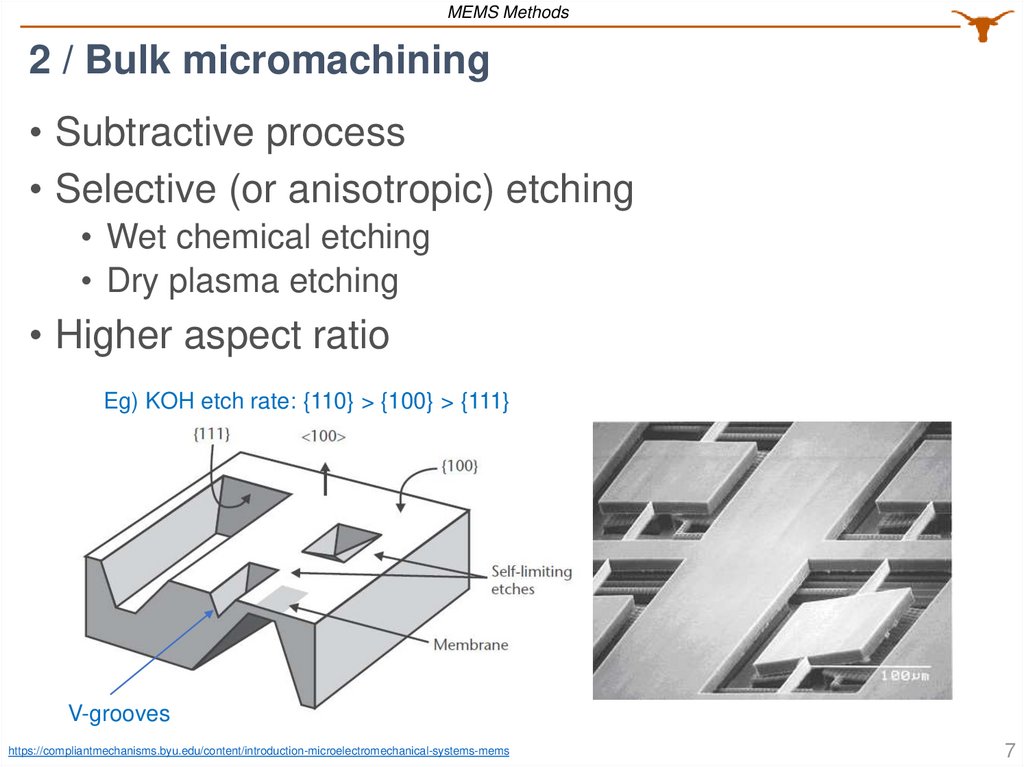
MEMS Methods2 / Bulk micromachining
• Subtractive process
• Selective (or anisotropic) etching
• Wet chemical etching
• Dry plasma etching
• Higher aspect ratio
Eg) KOH etch rate: {110} > {100} > {111}
V-grooves
https://compliantmechanisms.byu.edu/content/introduction-microelectromechanical-systems-mems
7
8.
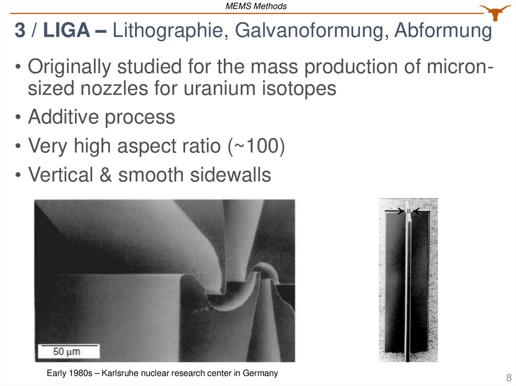
MEMS Methods3 / LIGA – Lithographie, Galvanoformung, Abformung
• Originally studied for the mass production of micronsized nozzles for uranium isotopes
• Additive process
• Very high aspect ratio (~100)
• Vertical & smooth sidewalls
Early 1980s – Karlsruhe nuclear research center in Germany
8
9.
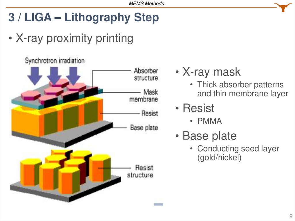
MEMS Methods3 / LIGA – Lithography Step
• X-ray proximity printing
• X-ray mask
• Thick absorber patterns
and thin membrane layer
• Resist
• PMMA
• Base plate
• Conducting seed layer
(gold/nickel)
9
10.
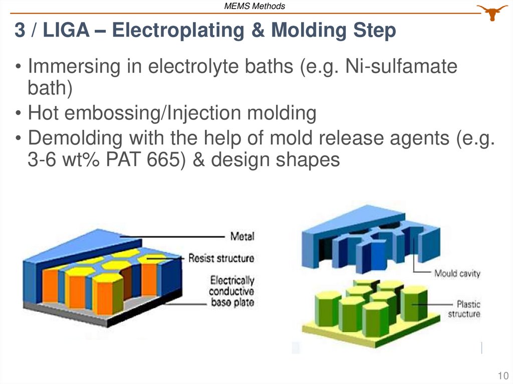
MEMS Methods3 / LIGA – Electroplating & Molding Step
• Immersing in electrolyte baths (e.g. Ni-sulfamate
bath)
• Hot embossing/Injection molding
• Demolding with the help of mold release agents (e.g.
3-6 wt% PAT 665) & design shapes
10
11.
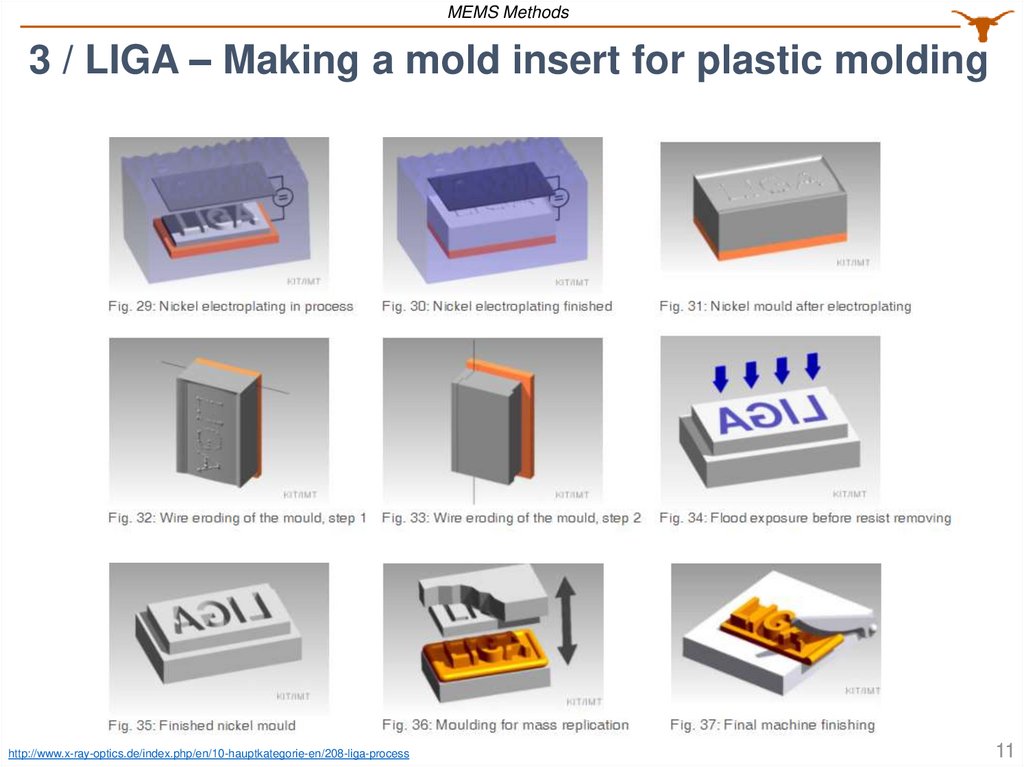
MEMS Methods3 / LIGA – Making a mold insert for plastic molding
http://www.x-ray-optics.de/index.php/en/10-hauptkategorie-en/208-liga-process
11
12.
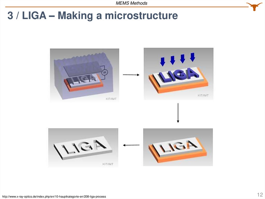
MEMS Methods3 / LIGA – Making a microstructure
http://www.x-ray-optics.de/index.php/en/10-hauptkategorie-en/208-liga-process
12
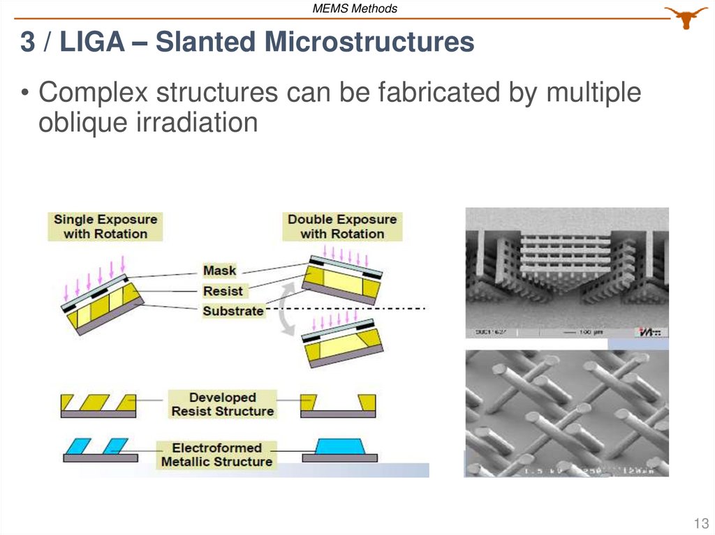
13.
MEMS Methods3 / LIGA – Slanted Microstructures
• Complex structures can be fabricated by multiple
oblique irradiation
13
14.
MEMS ApplicationsVarious applications of MEMS
• Industrial & automotive
Pressure sensors
Accelerometers
Nozzles
Safety devices for nuclear weapons
• Optical displays
• Digital micromirrors
14
15.
MEMS Applications1 / Industrial & automotive
• Piezoresistive pressure sensors
• Thin silicon diaphragm
• Mechanical stress causes changes in crystal lattice
structure electrical resistance changes
15
16.
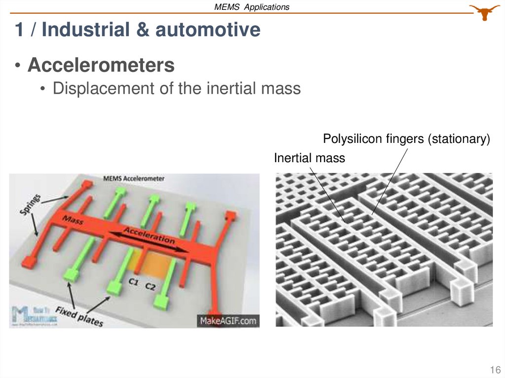
MEMS Applications1 / Industrial & automotive
• Accelerometers
• Displacement of the inertial mass
Polysilicon fingers (stationary)
Inertial mass
16
17.
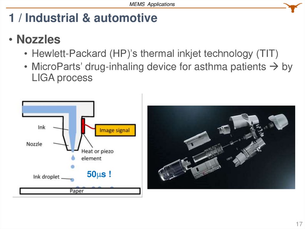
MEMS Applications1 / Industrial & automotive
• Nozzles
• Hewlett-Packard (HP)’s thermal inkjet technology (TIT)
• MicroParts’ drug-inhaling device for asthma patients by
LIGA process
50 s !
17
18.
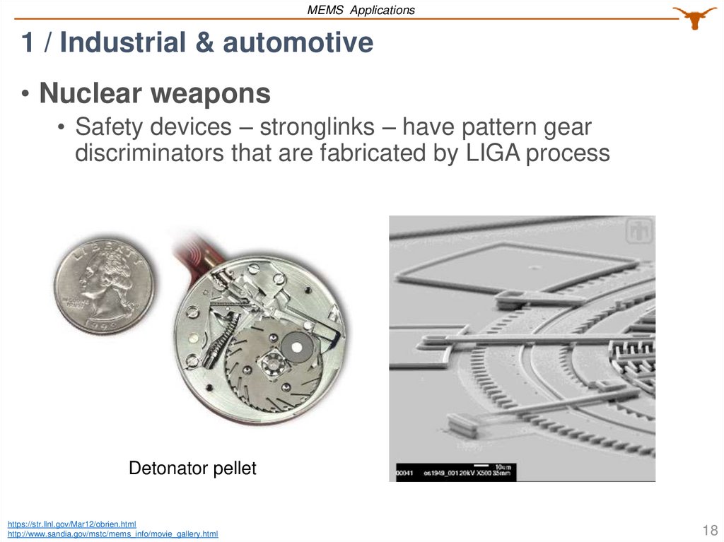
MEMS Applications1 / Industrial & automotive
• Nuclear weapons
• Safety devices – stronglinks – have pattern gear
discriminators that are fabricated by LIGA process
Detonator pellet
https://str.llnl.gov/Mar12/obrien.html
http://www.sandia.gov/mstc/mems_info/movie_gallery.html
18
19.
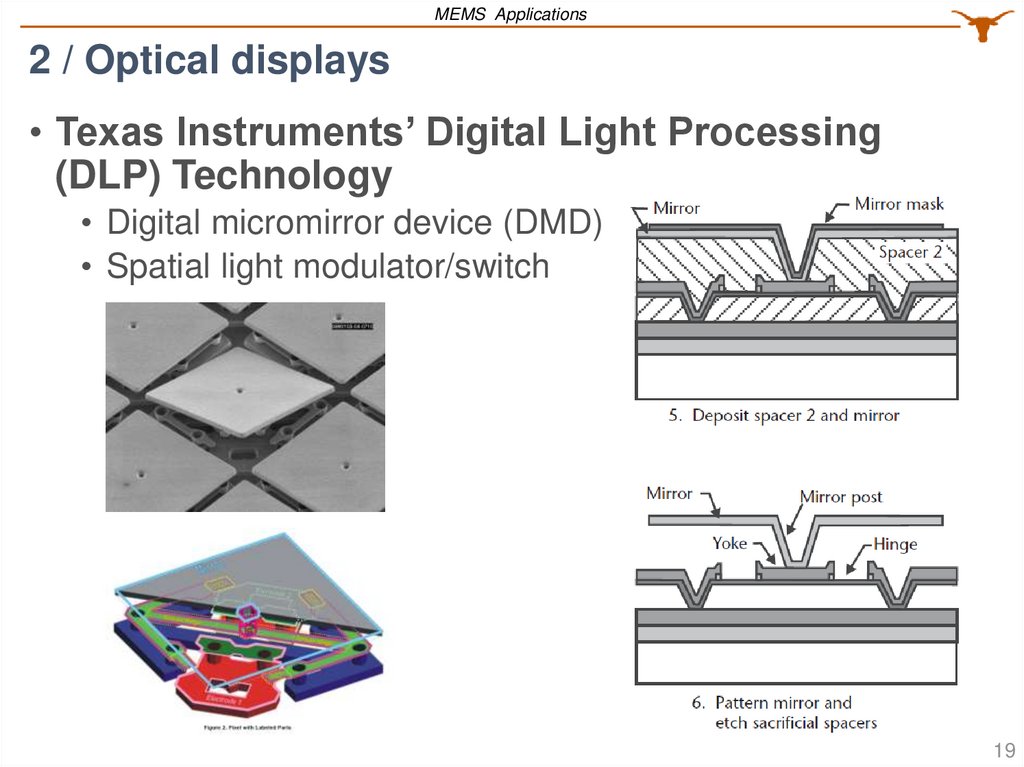
MEMS Applications2 / Optical displays
• Texas Instruments’ Digital Light Processing
(DLP) Technology
• Digital micromirror device (DMD)
• Spatial light modulator/switch
19
20.
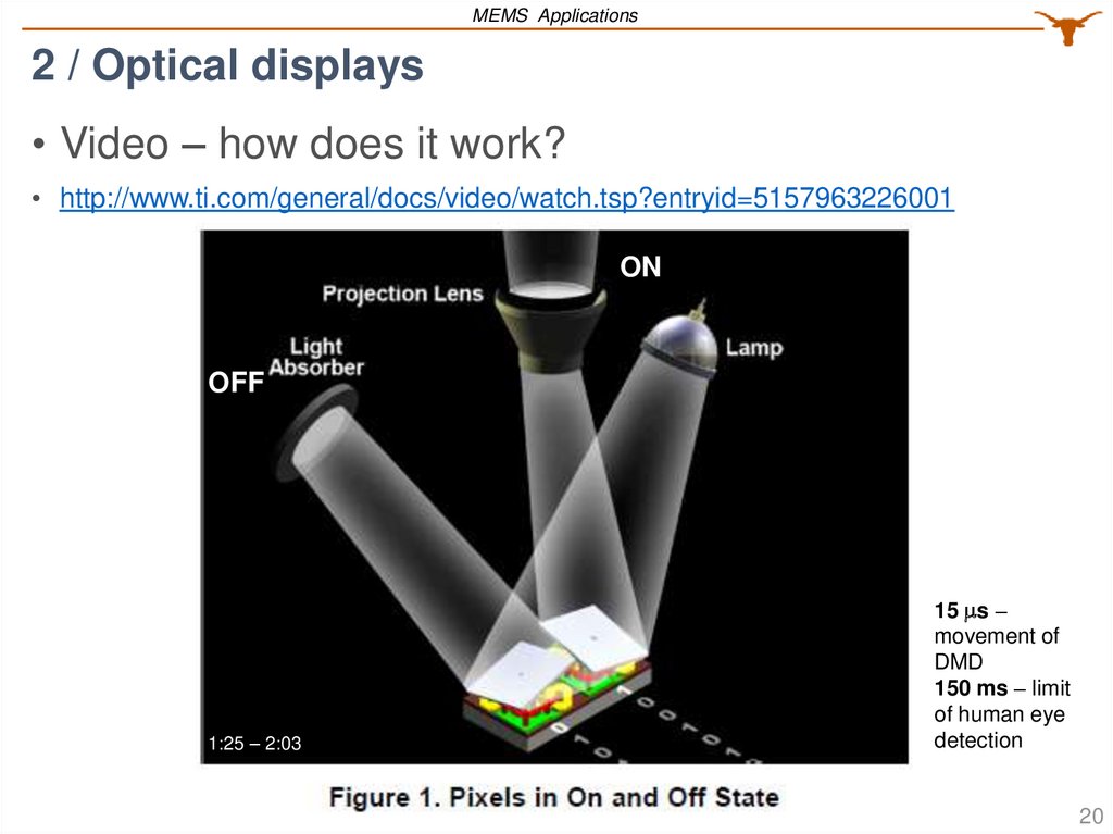
MEMS Applications2 / Optical displays
• Video – how does it work?
• http://www.ti.com/general/docs/video/watch.tsp?entryid=5157963226001
ON
OFF
1:25 – 2:03
15 s –
movement of
DMD
150 ms – limit
of human eye
detection
20
21.
MEMS Applications2 / Optical displays
• Reliability
• Hinge fatigue
• Shock & vibration failure
21
22.
Outlook of MEMSOutlook for MEMS
Strength
• Provides a customized technical solution for a
particular application
• Many tools to choose from
Limitation
• Doesn’t have any standards
• Not many high-volume manufacturing applications
Absence of “the killer app”
• Diverging demands & fragmentation
• Poor forecasting & investments
To MEMS or not to MEMS?
• Enabling a new function, cost reduction, reliability
22
23.
Thank YouCover of Scientific American Magazine in November 1992 (G. Stix, Scientific American 267, 5 (1992)). https://en.wikipedia.org/wiki/LIGA
23
24.
/ References /References
1.
2.
Gad-el-Hak, Mohamed, ed. The MEMS handbook. CRC press, 2001
Maluf, Nadim, and Kirt Williams. Introduction to microelectromechanical
systems engineering. Artech House, 2004
3. http://www.ece.umd.edu/class/enee416/GroupActivities/LIGA%20Presentat
ion.pdf
4. www.eng.utah.edu/~gale/mems/Lecture%2015%20LIGA.pdf
5. www.ti.com/lit/an/dlpa008a/dlpa008a.pdf
6. EFAB. Digital Image. Microfabrica, Inc. Web. 24 November 2016.
https://microfabrica.com
7. http://www.sandia.gov/mstc/mems/index.html
8. https://compliantmechanisms.byu.edu/content/introductionmicroelectromechanical-systems-mems
9. https://www.youtube.com/watch?v=EALXTht-stg
10. Plummer, David W. and Greenwood, William H. The History of Nuclear
Weapon Safety Devices. Sandia National Laboratories.
11. Wolfgang Ehrfeld, Electrochemistry and microsystems, In Electrochimica
Acta, Volume 48, Issues 20–22, 2003, Pages 2857-2868
24