


")


")


")


;")

 Электроника
Похожие презентации:


 Application Model")
Behavioral Modeling of Data
1. Behavioral Modeling of Data Converters using Verilog-A
George SuárezGraduate Student
Electrical and Computer Engineering
University of Puerto Rico, Mayaguez
Code 564: Microelectronics and Signal
Processing Branch
NASA Goddard Space Flight Center
2. Agenda
IntroductionVerilog-A
Objectives
Sample and Hold
Analysis
Jitter Noise
Thermal noise
Model
Simulation results
Generic DAC
Analysis and model
Dynamic element matching
Simulation results
2
Behavioral Modeling of ADCs using Verilog-A
by George Suárez
NASA Goddard Space Flight Center
Code 564 Microelectronic and Signal Processing
3. Agenda
Generic ADCAnalysis and model
Simulation results
Flash ADC
Analysis and model
Simulation results
SAR ADC
Analysis and model
Simulation Results
Pipelined ADC
Analysis
1.5 bit Stage
- 1.5 bit ADC
3
Behavioral Modeling of ADCs using Verilog-A
by George Suárez
NASA Goddard Space Flight Center
Code 564 Microelectronic and Signal Processing
4. Agenda
- 1.5 bit MDACDigital Correction
Simulation results
ΣΔ ADC
ΣΔ Modulator
- SC integrator analysis
- Model
- Simulation results
Conclusions
Future Work
Acknowledgements
References
4
Behavioral Modeling of ADCs using Verilog-A
by George Suárez
NASA Goddard Space Flight Center
Code 564 Microelectronic and Signal Processing
5. Introduction
Transistor-level modeling and simulation is the most accurateapproach for mixed-signal circuits.
It becomes impractical for complex systems due to the long
computational time required.
Cell View
No. of
Transistors
No. of
Equations
Simulation Time
436
1111
52 s
17601
125 ks
1 day, 10 hours,
42 min.
Transistor Level
7000
Taken form the article: Efficient Testing of Analog/Mixed-Signal ICs using Verilog-A
Nitin Mohan, Sirific Wireless www.techonline.com
5
Behavioral Modeling of ADCs using Verilog-A
by George Suárez
NASA Goddard Space Flight Center
Code 564 Microelectronic and Signal Processing
6. Introduction
This situation has led circuit designers to consider alternatemodeling techniques:
Approach
Accuracy
Speed
Flexibility
Device models
Custom C++ models
Finite-difference equations
Circuit-based macromodels
Cell View
No. of
Transistors
No. of
Equations
Simulation
Time
Transistor
Level
436
1111
52 s
Behavioral
270
697
4s
Time-domain macromodels
Behavioral models
Transistor
Level
7000
17601
125 ks
1 day, 10
hours, 42
min.
Behavioral
439
1148
124s
www.techonline.com Efficient Testing of Analog/MixedSignal ICs using Verilog-A, Nitin Mohan, Sirific Wireless
In addition, behavioral modeling can be effectively used in a
top-down design approach.
6
Behavioral Modeling of ADCs using Verilog-A
by George Suárez
NASA Goddard Space Flight Center
Code 564 Microelectronic and Signal Processing
7. Introduction
System Level(Matlab, C++,
SystemC, AHDLs,
etc…)
Phase
comparator
Loop filter
F(s)
VCO
Functional Level
(SPICE, AHDLs)
A=1
A=1
Behavioral models
fo
--
Vout
Vin
+
V-
V+
Transistor Level
(SPICE)
Layout
Top-Down Design Approach
7
Behavioral Modeling of ADCs using Verilog-A
by George Suárez
NASA Goddard Space Flight Center
Code 564 Microelectronic and Signal Processing
8. Verilog-A
The Verilog-A is a high-level language developed to describe the structureand behavior of analog systems and their components.
It is an extension to the IEEE 1364 Verilog HDL specification for digital
design.
The analog systems are described in Verilog-A in a modular way using
hierarchy and different levels of modeling complexity.
The motivation is to invest in a new higher level of abstraction in analog
design and its combination with the digital one.
`include "constants.vams"
`include "disciplines.vams"
vin
vref
vout
module COMP (vin, vref, vout);
output vout;
electrical vout;
input vin;
electrical vin;
input vref;
electrical vref;
parameter real slope = 100.0;
parameter real offset = 0.0 ;
8
Behavioral Modeling of ADCs using Verilog-A
by George Suárez
NASA Goddard Space Flight Center
Code 564 Microelectronic and Signal Processing
9. Objectives
Build a set of analog and mixed-signal behavioral models usingthe Verilog-A AHDL, that allows a high level simulation of
ADCs.
Simulate some popular ADCs architectures such as:
Flash ADC
SAR ADC
Pipelined ADC
Simulate other common used mixed-signal circuits such as:
ΣΔ Modulator
Sample and Hold
Provide a general modeling approach for noise sources and
other non-idealities.
Provide performance results for the simulated data converters
such as spectrum measures SNR, SNDR, THD etc.
9
Behavioral Modeling of ADCs using Verilog-A
by George Suárez
NASA Goddard Space Flight Center
Code 564 Microelectronic and Signal Processing
10. Agenda
IntroductionVerilog-A
Objectives
Sample and Hold
Analysis
Jitter Noise
Thermal noise
Model
Simulation results
Generic DAC
Analysis and model
Dynamic element matching
Simulation results
10
Behavioral Modeling of ADCs using Verilog-A
by George Suárez
NASA Goddard Space Flight Center
Code 564 Microelectronic and Signal Processing
11. Sample and Hold
Φs1Cs
Ron
Vin
Φs1
Thermal noise
Vth ≈ kT/Cs
(Opamp noise neglected)
δ
Vout
-
1 – exp[-t / (2RonCs)]
Cp
+
CL
Jitter
x(t+δ) - x(t) ≈ δ
d
x(t)
dt
• Finite DC gain A0
• Finite GBW
• Cp and CL
Ideal
value
Vout
• Defective settling
• Linear
• Slewing
• Partial Slewing
εg= 1 - Cs /[ Cs + (Cs + Cp)/A0]
2
ωp
H(s)
ω
2
s 2 p s ωp
Qp
ω p 2π GBW
Cs
Cs C p
|H|
Φs1
Time
f
Behavioral Modeling of ADCs using Verilog-A
by George Suárez
11
NASA Goddard Space Flight Center
Code 564 Microelectronic and Signal Processing
12. Jitter Noise
Clock jitter is due to the non-uniform sampling of the inputδ
signal.
ΔV
The magnitude of this error is a function of the statistical
properties of the jitter and the input signal to the system.
In sampled data systems, when a sinusoidal input is taken, the
error introduced by jitter can be modeled by,
x(t+δ) - x(t) ≈ 2πfinδAcos(2πfinnt) ≈ δ
d
x(t)
dt
where δ is the sampling uncertainty, this is taken to be a
Gaussian random process with standard deviation Δt.
12
Behavioral Modeling of ADCs using Verilog-A
by George Suárez
NASA Goddard Space Flight Center
Code 564 Microelectronic and Signal Processing
13. Jitter Noise
It is assumed that is a Gaussian random process with zero mean and standard deviation Δt.Δt
-Δt
Statistical properties of the jitter
Input signal to the system
0
0
3.01MHz
301 kHz
30.1kHz
-20
100 ps
1 ns
10 ns
-20
M a g n itu d e (d B )
M a g n itu d e (d B )
-40
-60
-80
-100
-40
-60
-80
-120
-100
-140
-120
-160
-180
0
0.5
1
1.5
2
2.5
3
Frequency (Hz)
3.5
4
4.5
5
6
x 10
-140
0
0.5
1
1.5
2
2.5
3
Frequency (Hz)
3.5
4
4.5
5
6
x 10
13
Behavioral Modeling of ADCs using Verilog-A
by George Suárez
NASA Goddard Space Flight Center
Code 564 Microelectronic and Signal Processing
14. Thermal Noise
Thermal noise in circuits is because of the randomfluctuation of carriers due to thermal energy.
Proportional to the temperature.
It is assumed to be a Gaussian random process with zero
mean.
0
27 oC
0 oC
-30 oC
-20
-40
27 oC
0 oC
-30 oC
-123
-124
-126
Magnitude (dB)
M a g n itud e (d B )
-125
-60
-80
-100
-127
-128
-129
-120
-130
-140
-131
-160
-132
1.98
-180
0
0.5
1
1.5
2
2.5
Frequency (Hz)
3
3.5
2
2.02
2.04
2.06
Frequency (Hz)
4
2.08
2.1
6
x 10
6
x 10
14
Behavioral Modeling of ADCs using Verilog-A
by George Suárez
NASA Goddard Space Flight Center
Code 564 Microelectronic and Signal Processing
15. Sample and Hold model
ThermalNoise
Ideal S&H
Vin
Filter
Jitter
+
τ = RonCs
Defective
settling
Vout
Vout
Ideal
Nonideal
15
Behavioral Modeling of ADCs using Verilog-A
by George Suárez
NASA Goddard Space Flight Center
Code 564 Microelectronic and Signal Processing
16. Sample and Hold simulation results
PSD for sampled signal of 0 dB, fin = 2.5146MHz N = 8192, BW = 25MHz0
Ideal
Nonideal
-20
-40
Magnitude (dB )
-60
Increase in noise floor due nonidealities
-80
-100
-120
-140
-160
-180
-200
0
0.5
1
1.5
Frequency (Hz)
2
2.5
7
x 10
16
Behavioral Modeling of ADCs using Verilog-A
by George Suárez
NASA Goddard Space Flight Center
Code 564 Microelectronic and Signal Processing
17. Agenda
IntroductionVerilog-A
Objectives
Sample and Hold
Analysis
Jitter Noise
Thermal noise
Model
Simulation results
Generic DAC
Analysis and model
Dynamic element matching
Simulation results
17
Behavioral Modeling of ADCs using Verilog-A
by George Suárez
NASA Goddard Space Flight Center
Code 564 Microelectronic and Signal Processing
18. Generic DAC
B bits2B-1
unit
2B-2
1
Vout
+
unit
0.0% DAC mismatch DEM off
0.1% DAC mismatch DEM off
…
Mismatch in DAC units.
INL
Gain error
Offset
Thermometer decoder
Generic DAC
unit
0
unit
Mismatch in capacitors!
(trimming can reduced it to 0.1%
Increase in harmonics content)
Generic DAC model
including mismatch in units
0
-20
2C
6
2C
2
2C
1
C
C
Dummy
+
-40
Magnitude (dB)
MSB
27C
Vin
Vref
Gnd
-60
-80
-100
-120
SAR Capacitive DAC, SAH and comparator
-140
0
0.5
1
1.5
Frequency (Hz)
2
2.5
x 10
5
18
Behavioral Modeling of ADCs using Verilog-A
by George Suárez
NASA Goddard Space Flight Center
Code 564 Microelectronic and Signal Processing
19. Generic DAC model
nominal gainεg
Gain error
q
Quantization step
INL
Integral non-linearity
εoff
Offset error
FS
Full scale voltage
l1
-FS/(2g)
q
FS/(2N-1)
A
(2N-1-1)q
α
1/(1+q εg)
offset
(l1 εg-εoff)q
ε0
(INL)sqrt(27)/(2N-2)
wa
(1- ε0)xa + xa3 ε0/A2
ya
α(wa + off)
vadc
N bits
DAC
with
mismatch
xa
wa
α
va
+
offset
Ideal
Nonideal
Offset error = 0.5LSB
Analog output
g
Gain error = 0.5LSB
INL = 0.5LSB
Digital input code
19
Behavioral Modeling of ADCs using Verilog-A
by George Suárez
NASA Goddard Space Flight Center
Code 564 Microelectronic and Signal Processing
20. DEM
Spread the mismatch errorenergy across the spectrum
generating white or colored noise
in the DAC output.
Magnitude (dB)
Due to design complexity and non-scalability for modeling purposes it is easier to implement a
general stochastic approach using randomization.
Magnitude (dB)
Improve the DAC performance by
locating the distortion caused by the
component mismatch errors in certain
frequency bands.
f (Hz)
Magnitude (dB)
Dynamic Element Matching (DEM) techniques are used to minimize the effect of DAC units
mismatch.
DAC DEM techniques can be divided in deterministic and stochastic.
Magnitude (dB)
f (Hz)
f (Hz)
20
Behavioral Modeling of ADCs using Verilog-A
by George Suárez
NASA Goddard Space Flight Center
Code 564 Microelectronic and Signal Processing
21. DEM simulation results
0…
Randomize
unit
1
DAC 0.1% mismatch
unit
2B-2
…
…
B bits
Thermometer decoder
2B-1
+
Vout
0
0.1% DAC mismatch DEM off
-20
DEM off
-40
unit
-60
-80
unit
-100
In Verilog-A its rather simple to randomize uniformly the
units. Assuming we have a system clock, for each rising
edge of the clock signal we randomize the units.
-120
-140
Magnitude (dB)
By randomizing the DAC units (i.e. using a digital circuitry
FSM with a system clock) the effect of the mismatch in the
spectrum is reduced by reducing the harmonic distortion.
0
0.5
1
1.5
2
2.5
5
x 10
0
0.1% DAC mismatch DEM on
-20
DEM on
-40
-60
-80
if(DEM_enable) begin
generate i(1,`DAC_UNITS) begin
temp = $dist_uniform(seed, 1, `DAC_UNITS);
-100
-120
-140
if(temp - floor(temp) >= 0.5)
DEM[i] = ceil(temp);
else
DEM[i] = floor(temp);
0
0.5
1
1.5
2
2.5
5
Frequency (Hz)
x 10
end
end
// Then select units stored in the array DEM[ ] for conversion
Behavioral Modeling of ADCs using Verilog-A
by George Suárez
21
NASA Goddard Space Flight Center
Code 564 Microelectronic and Signal Processing
22. Agenda
Generic ADCAnalysis and model
Simulation results
Flash ADC
Analysis and model
Simulation results
SAR ADC
Analysis and model
Simulation Results
Pipelined ADC
Analysis
1.5 bit Stage
- 1.5 bit ADC
22
Behavioral Modeling of ADCs using Verilog-A
by George Suárez
NASA Goddard Space Flight Center
Code 564 Microelectronic and Signal Processing
23. Generic ADC model
gnominal gain
εg
Gain error
q
Quantization step
INL
Integral non-linearity
εoff
Offset error
FS
Full scale voltage
q
FS/(2 -1)
l1
-FS/(2g) + q/2
A
(2N-1-1)q
α
1/(1+qεg)
offset
(l1 εg-εoff)q
ε0
(INL)sqrt(27)/(2N-2)
wa
α(wa + off)
ya
(1- ε0)xa + xa3 ε0/A2
va
+
α
wa
xa
Ideal
ADC
N bits
vadc
offset
Ideal
Nonideal
Offset error = 0.5LSB
Digital output code
N
Gain error = 0.5LSB
INL = 0.5LSB
Analog input
23
Behavioral Modeling of ADCs using Verilog-A
by George Suárez
NASA Goddard Space Flight Center
Code 564 Microelectronic and Signal Processing
24. Generic ADC simulation results
PSD plot for 8-bit generic ADC with 0 dB input signal f in of 500.977KHz, Samples = 8192, BW = 2MHzM a g n itu d e (d B )
0
SNDR =
SNR =
THD =
SFDR =
ENOB =
-20
-40
49.82 dB
49.90 dB
-64.668 dB
67.461 dB
8 bits
-60
-80
-100
-120
0
0.2
0.4
0.6
0.8
1
1.2
1.4
1.6
1.8
Frequency (Hz)
SNDR = 47.877 dB
0
M a g n itu d e (d B )
2
6
x 10
SNR = 49.455 dB
THD = -53.037 dB
SFDR = 53.859 dB
ENOB
= 7.7= bits
gain error =0.5LSB, offset error = 0.5LSB
and INL
0.5LSB
-20
-40
-60
-80
-100
-120
0
0.2
0.4
0.6
0.8
1
Frequency (Hz)
1.2
1.4
1.6
1.8
2
6
x 10
24
Behavioral Modeling of ADCs using Verilog-A
by George Suárez
NASA Goddard Space Flight Center
Code 564 Microelectronic and Signal Processing
25. Agenda
Generic ADCAnalysis and model
Simulation results
Flash ADC
Analysis and model
Simulation results
SAR ADC
Analysis and model
Simulation Results
Pipelined ADC
Analysis
1.5 bit Stage
- 1.5 bit ADC
25
Behavioral Modeling of ADCs using Verilog-A
by George Suárez
NASA Goddard Space Flight Center
Code 564 Microelectronic and Signal Processing
26. Flash ADC
+VrefR
R
+
-
R
+
R
…
…
…
…
Are made by cascading highspeed comparators.
Are the fastest way to convert an
analog signal to a digital signal.
Ideal for applications requiring
very large bandwidth.
Typically consume more power
than other ADC architectures and
are generally limited to 8-bits
resolution.
Decoder
N bits
R
+
-
R
+
-Vref
26
Behavioral Modeling of ADCs using Verilog-A
by George Suárez
NASA Goddard Space Flight Center
Code 564 Microelectronic and Signal Processing
27. Flash ADC non-idealities
OPAMPFinite DC gain
Finite GBW
Input resistance
Output resistance
Bias current
Offset voltage
Slew Rate
Vdd
GBW = gm1/CC
I5 = SR*Cc
Ibias
V-
V+
I5
Cc
CL
Bubbles
Cadence provides a well accepted
behavioral model of an non-ideal OPAMP/
It is due the metastability of the
comparators. (Future work will try OTA for the most used AHDLs (Verilog-A,
Verilog-AMS and VHDL-AMS)!
model this effect)
27
Behavioral Modeling of ADCs using Verilog-A
by George Suárez
NASA Goddard Space Flight Center
Code 564 Microelectronic and Signal Processing
28. Flash ADC simulation results
PSD plot for 8-bit Flash ADC with 0 dB input signal f in of 3.01MHz, Samples = 4096, BW = 5MHz0
Ideal
Nonideal
-10
-20
M a g n itu d e (d B )
-30
-40
-50
SNDR (dB)
49.264
44.408
SNR (dB)
49.323
44.481
THD (dB)
-67.954
-62.193
SFDR (dB)
60.778
47.261
ENOB
7.9
7.1
-60
-70
-80
-90
-100
-110
0
0.5
1
1.5
2
2.5
Frequency (Hz)
3
3.5
4
4.5
5
6
x 10
28
Behavioral Modeling of ADCs using Verilog-A
by George Suárez
NASA Goddard Space Flight Center
Code 564 Microelectronic and Signal Processing
29. Agenda
Generic ADCAnalysis and model
Simulation results
Flash ADC
Analysis and model
Simulation results
SAR ADC
Analysis and model
Simulation Results
Pipelined ADC
Analysis
1.5 bit Stage
- 1.5 bit ADC
29
Behavioral Modeling of ADCs using Verilog-A
by George Suárez
NASA Goddard Space Flight Center
Code 564 Microelectronic and Signal Processing
30. SAR ADC
Successive-approximation-register (SAR) ADCs) used formedium-to-high-resolution (8 to 16 bits) applications with
sample rates under 5 Msps.
Used in portable/battery-powered instruments, pen digitizers,
industrial controls, and data/signal acquisition.
Provide low power consumption.
An N-bit SAR ADC will require N comparison periods and will
not be ready for the next conversion until the current one is
complete.
30
Behavioral Modeling of ADCs using Verilog-A
by George Suárez
NASA Goddard Space Flight Center
Code 564 Microelectronic and Signal Processing
31. SAR ADC
StartCLK
EOC
CONV
Timing
control
SAH
Vin
Sample
& hold
Successive
Approximation
Register
(SAR)
+
-
Anti-aliased signal
N bits
DAC
VDAC
N bits
Register
Vref
¾ Vref
CLK
½ Vref
Start
Vin
¼ Vref
SAH
time
bit 3=0
(MSB)
bit 2=1 bit 1=0 bit 0=1
(LSB)
CONV
Conversion time
EOC
31
Behavioral Modeling of ADCs using Verilog-A
by George Suárez
NASA Goddard Space Flight Center
Code 564 Microelectronic and Signal Processing
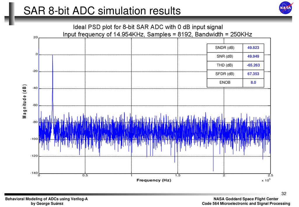
32.
SAR 8-bit ADC simulation resultsIdeal PSD plot for 8-bit SAR ADC with 0 dB input signal
Input frequency of 14.954KHz, Samples = 8192, Bandwidth = 250KHz
20
0
M a g n itu d e (d B )
-20
SNDR (dB)
49.823
SNR (dB)
49.949
THD (dB)
-65.263
SFDR (dB)
67.353
ENOB
8.0
-40
-60
-80
-100
-120
-140
0
0.5
1
1.5
Frequency (Hz)
2
2.5
x 10
5
32
Behavioral Modeling of ADCs using Verilog-A
by George Suárez
NASA Goddard Space Flight Center
Code 564 Microelectronic and Signal Processing
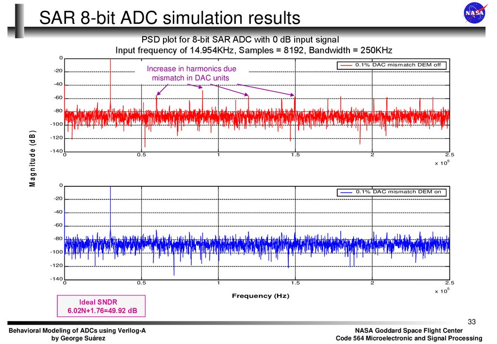
33.
SAR 8-bit ADC simulation resultsPSD plot for 8-bit SAR ADC with 0 dB input signal
Input frequency of 14.954KHz, Samples = 8192, Bandwidth = 250KHz
0
0.1% DAC mismatch DEM off
Increase in harmonics due
mismatch in DAC units
-20
-40
-60
-80
M a g n itu d e (d B )
-100
-120
-140
0
0.5
1
1.5
2
2.5
5
x 10
0
0.1% DAC mismatch DEM on
-20
-40
-60
-80
-100
-120
-140
0
0.5
1
1.5
2
2.5
5
Ideal SNDR
6.02N+1.76=49.92 dB
Frequency (Hz)
x 10
33
Behavioral Modeling of ADCs using Verilog-A
by George Suárez
NASA Goddard Space Flight Center
Code 564 Microelectronic and Signal Processing
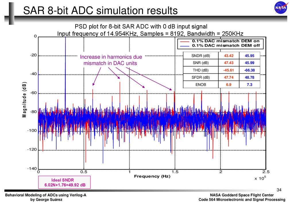
34.
SAR 8-bit ADC simulation resultsPSD plot for 8-bit SAR ADC with 0 dB input signal
Input frequency of 14.954KHz, Samples = 8192, Bandwidth = 250KHz
0
0.1% DAC mismatch DEM on
0.1% DAC mismatch DEM off
-20
Increase in harmonics due
mismatch in DAC units
M a g n itu d e (d B )
-40
SNDR (dB)
43.42
45.95
SNR (dB)
47.43
45.99
THD (dB)
-45.61
-66.38
SFDR (dB)
47.74
48.78
ENOB
6.9
7.3
-60
-80
-100
-120
-140
0
0.5
Ideal SNDR
6.02N+1.76=49.92 dB
1
1.5
Frequency (Hz)
2
2.5
5
x 10
34
Behavioral Modeling of ADCs using Verilog-A
by George Suárez
NASA Goddard Space Flight Center
Code 564 Microelectronic and Signal Processing
35. Agenda
Generic ADCAnalysis and model
Simulation results
Flash ADC
Analysis and model
Simulation results
SAR ADC
Analysis and model
Simulation Results
Pipelined ADC
Analysis
1.5 bit Stage
- 1.5 bit ADC
35
Behavioral Modeling of ADCs using Verilog-A
by George Suárez
NASA Goddard Space Flight Center
Code 564 Microelectronic and Signal Processing
36. Agenda
- 1.5 bit MDACDigital Correction
Simulation results
ΣΔ ADC
ΣΔ Modulator
- SC integrator analysis
- Model
- Simulation results
Conclusions
Future Work
Acknowledgements
References
36
Behavioral Modeling of ADCs using Verilog-A
by George Suárez
NASA Goddard Space Flight Center
Code 564 Microelectronic and Signal Processing
37. Pipelined ADC
Has become the most popular ADC architecture for samplingrates from a few MS/s up to 100MS/s, with resolutions from 8
bits at the faster sample rates up to 16 bits at the lower rates.
Low-power capability.
Allows the use of "digital error correction" and “digital
calibration” to greatly reduce the accuracy requirement of the
internal flash ADCs and DACs respectively.
Because each sample has to propagate through the entire
pipeline before all its associated bits are available there is
some data latency.
37
Behavioral Modeling of ADCs using Verilog-A
by George Suárez
NASA Goddard Space Flight Center
Code 564 Microelectronic and Signal Processing
38. Pipeline ADC
M bitsDigital correction
N1 bits
N2 bits
Nk-1 bits
Nk bits
Nk-1 bits
Nk bits
Registers
N1 bits
Sample
& hold
Stage1
N2 bits
Stage2
Stagek-1
+
Nk-1 bits
Nk-1bit
ADC
+
-
Nk-1bit
DAC
Stagek
2N
k-1
Residue amplifier
38
Behavioral Modeling of ADCs using Verilog-A
by George Suárez
NASA Goddard Space Flight Center
Code 564 Microelectronic and Signal Processing
39. Pipeline ADC 8-bit (1.5-bit per stage )
dout8 bits
Digital correction
2 bit
2 bit
2 bit
2 bits
2 bit
2 bits
Φ1
Registers
Φ2
2 bit
Vin
Anti-aliased
signal
Sample
& hold
Φ1
2 bit
Stage1
Stage2
Φ2
Φ1
Stage6
Φ1
1.5 bit
ADC
Φ2
Φ1
Φ2
39
Behavioral Modeling of ADCs using Verilog-A
by George Suárez
NASA Goddard Space Flight Center
Code 564 Microelectronic and Signal Processing
40. 1.5-bit Pipelined Stage
1.5 bit ADCMDAC
Vin
+
2 bits
1.5 bit
ADC
1.5 bit
DAC
+
-1/4Vref
Encoder
+
Vin
Φ1
2 bits
Vr
Residue
Residue amplifier
Φ1
Vin
1/4Vref
2
+
Φ2
Φ2
Φ1
C2
-
C1
+
Residue
X
4:1
MUX
1/2Vref
0
-1/2Vref
Φ1
Φ2
b1 b0
From ADC
40
Behavioral Modeling of ADCs using Verilog-A
by George Suárez
NASA Goddard Space Flight Center
Code 564 Microelectronic and Signal Processing
41. 1.5-bit ADC
+2 bits
-
1.5 bit
ADC
+
Vin
+
Encoder
1/4Vref
1.5 bit
DAC
2 bits
2
+
Residue amplifier
Digital code
1.5 bit ADC
10
01
00
-1/4Vref
-
-1/4Vref
1/4Vref
Vin
Modeled as a Generic ADC with the
specified reference levels
41
Behavioral Modeling of ADCs using Verilog-A
by George Suárez
NASA Goddard Space Flight Center
Code 564 Microelectronic and Signal Processing
42. 1.5-bit MDAC
MDACVin
Residue
+
+
2 bits
1.5 bit
ADC
Φ1
Vin
1.5 bit
DAC
Φ2
Residue amplifier
Vres = Vin(C1+C2)/C1 + Vr
Residue
Φ1
Vr
-
2
Φ2
Φ1
C2
Vref
1/2Vref
-
C1
+
X
4:1
MUX
1/2Vref
0
-1/2Vref
0
Residue
Vin
-1/2Vref
-Vref
Φ1
Φ2
-1/4Vref
-1/4Vref
b1 b0
From ADC
42
Behavioral Modeling of ADCs using Verilog-A
by George Suárez
NASA Goddard Space Flight Center
Code 564 Microelectronic and Signal Processing
43. 1.5-bit MDAC nonidealities
Φ1Capacitors mismatch
Φ1
Φ2
C2 C1 C
Φ2
Φ1
C2
C1
Cp
+
CL
|H|
Vin
X
Thermal noise Vth ≈ kT/C1
(Opamp noise neglected)
4:1
MUX
From ADC
1/2Vref
0
-1/2Vref
Φ1
Φ2
• Finite DC gain A0
Ideal
value
Vres
• Finite GBW, Cp and CL
Time
• Defective settling
• Linear
• Slewing
• Partial Slewing
εg= C1+(C1+ C2+ Cp)/A0
2
ωp
H(s)
ω
2
s 2 p s ωp
Qp
ω p 2 GBW
C1
C1 C2 C p
43
Behavioral Modeling of ADCs using Verilog-A
by George Suárez
NASA Goddard Space Flight Center
Code 564 Microelectronic and Signal Processing
44. 1.5-bit Stage model
ThermalNoise
Vin
+
1.5 bit
GenericADC
VADC
1.5bit MDAC
Including
mismatch
Defective
settling
Vres
2-bits
Ideal
Nonideal
44
Behavioral Modeling of ADCs using Verilog-A
by George Suárez
NASA Goddard Space Flight Center
Code 564 Microelectronic and Signal Processing
45. Digital Correction
Overflowcout
a
b[7]
b[6]
b[5]
b[4]
b[3]
b[2]
b[1]
sum
sum
sum
sum
sum
sum
sum
+
cin
b
cout
a
+
cin
b
cout
a
+
cin
b
cout
a
+
cin
b
cout
a
+
cin
b
cout
a
Register
Register
Register
Register
Register
Register
Register
Register
Register
Register
+
cin
b
cout
a
+
b[0]
cin
b
Register
s1[1] s1[0]
s2[1] s2[0]
Register
Register
Register
Register
s3[1] s3[0]
Register
Register
Register
s4[1] s4[0]
Register
Register
s5[1] s5[0]
Register
s6[1] s6[0]
Φ2
Φ1
s7[1] s7[0]
sk[1] sk[0] are the bits from stage k
45
Behavioral Modeling of ADCs using Verilog-A
by George Suárez
NASA Goddard Space Flight Center
Code 564 Microelectronic and Signal Processing
46. Pipelined 8-bit ADC model (Cadence)
46Behavioral Modeling of ADCs using Verilog-A
by George Suárez
NASA Goddard Space Flight Center
Code 564 Microelectronic and Signal Processing
47. Pipelined 8-bit ADC simulation results
PSD plot for 8-bit Pipelined ADC with 0 dB input signalInput frequency of 1.01MHz, Samples = 8192, Bandwidth = 5MHz
0
Non-ideal
Ideal
-20
M a g n itu d e (d B )
-40
SNDR (dB)
44.922
48.577
SNR (dB)
49.573
49.238
THD (dB)
-49.923
-57.082
SFDR (dB)
54.427
61.778
ENOB
7.2
7.8
-60
-80
-100
-120
-140
0
0.5
1
1.5
2
2.5
Frequency (Hz)
3
3.5
4
4.5
5
6
x 10
47
Behavioral Modeling of ADCs using Verilog-A
by George Suárez
NASA Goddard Space Flight Center
Code 564 Microelectronic and Signal Processing
48. Agenda
- 1.5 bit MDACDigital Correction
Simulation results
ΣΔ ADC
ΣΔ Modulator
- SC integrator analysis
- Model
- Simulation results
Conclusions
Future Work
Acknowledgements
References
48
Behavioral Modeling of ADCs using Verilog-A
by George Suárez
NASA Goddard Space Flight Center
Code 564 Microelectronic and Signal Processing
49. ΣΔ ADC
Makes use of oversampling and ΣΔ modulation techniques toachieve high resolution.
Used for low bandwidth and high-resolution applications but
recently there is great interest for medium to high bandwidth
applications.
Due oversampling the requirements of the anti-aliasing filter
are reduced.
fs
xi(t)
Anti-alias filter
xb(t)
x[n]
y[n]
Modulator
Analog
Digital
Filter
yo[n]
Digital
49
Behavioral Modeling of ADCs using Verilog-A
by George Suárez
NASA Goddard Space Flight Center
Code 564 Microelectronic and Signal Processing
50. ΣΔ Modulator (ΣΔM)
ΣΔM is the major analog component of the ADC.Due to its mixed-signal nature, non-idealities largely affect the
performance of the ADC, i.e. the integrator, DAC mismatch.
Quatization noise is shaped outside the band of interest.
Several architectures exists depending on the number of
integrators and the quantizer levels.
g1
g2
∫
Single or Multi-bit
depending on the
quantizer
N-level
Quantize
r
DAC
Digital Filter
Magnitude (dB)
Lth order contains L integrators
Signal
White
Noise
Shaped
Quantization
Noise
Frequency (Hz)
Behavioral Modeling of ADCs using Verilog-A
by George Suárez
50
NASA Goddard Space Flight Center
Code 564 Microelectronic and Signal Processing
51. SC integrator transient model
Single pole OTA modelDefective settling due to the OTA finite DC
gain, GBW and SR limitations.
Possible settling scenarios:
Linear
• |Vai| ≤ Io/gm
Φ 1 Ci
Vi
Φ2
Φ1
Va
Vr Φ1 Cr Φ2
Φ2
Φ1
Φ2
Cint
Φ2
Cp
Φ1
Vo
-
Φ1 Cinxt
OTA
+
CL
Φ2
Slewing
• |Vai| > Io/gm and t < to
Partial Slewing
Parameter
Description
Ci, Cr
Sampling capacitors
Cint
Integrating capacitor
Cp,Co
Input and output parasitic capacitances
Cinxt
Next stage input capacitance
gm
OTA transconductance
go
OTA output conductance
Io
OTA max output current
to
slewing time
Vai
Initial voltage at Va
Behavioral Modeling of ADCs using Verilog-A
by George Suárez
+Io
Va
go
-gmVa
Co
-Io
Ideal
value
settling error
Va
• |Vai| > Io/gm and t ≥ to
Vo
Integration Φ2
Sampling Φ1
Time
51
NASA Goddard Space Flight Center
Code 564 Microelectronic and Signal Processing
52. Second-Order ΣΔΜ Model
gX1 = Ci/CintgX2 = Cr/Cint
Φ2
OTA + switches for both
phases Φ1 and Φ2
Thermal
Noise
Vin
Jitter
+
Va
Vr Φ1 Cr Φ2
Cp
Φ1
C
Vo Φ1 inxt
OTA
+
Φ2
CL
Thermal
Noise
SC intg
SC intg
g11
g21
g12
0.1% mismatch
Φ1
Φ2
Φ1
Φ2
Cint
Vi Φ1 Ci Φ2
DAC
∫
+
g22
∫
5-level 3-bits
Flash ADC
3-bits
DAC
4-bits
4-bits
ILA
Decoder
4-bits
52
Behavioral Modeling of ADCs using Verilog-A
by George Suárez
NASA Goddard Space Flight Center
Code 564 Microelectronic and Signal Processing
53. ΣΔΜ Simulation Results GSM mode
*Second order sigma-delta modulator with -6 dB input signalInput frequency of 30kHz, OSR = 65, N = 65536, BW = 200kHz (GSM mode)
VHDL-AMS 74.0164 dB
Actual data 74.5000 dB
0.65% error
*This work has been accepted as a lecture presentation at the IEEE MWCAS 2005 conference, August 7-10 Cincinnati, Ohio.
53
Behavioral Modeling of ADCs using Verilog-A
by George Suárez
NASA Goddard Space Flight Center
Code 564 Microelectronic and Signal Processing
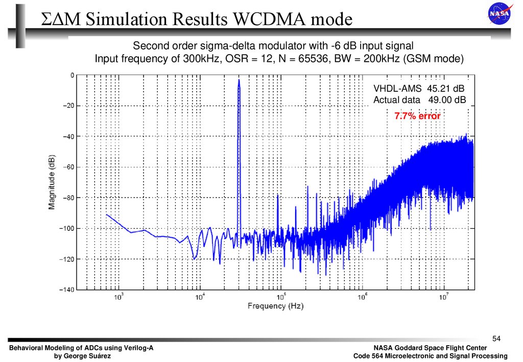
54.
ΣΔΜ Simulation Results WCDMA modeSecond order sigma-delta modulator with -6 dB input signal
Input frequency of 300kHz, OSR = 12, N = 65536, BW = 200kHz (GSM mode)
VHDL-AMS 45.21 dB
Actual data 49.00 dB
7.7% error
54
Behavioral Modeling of ADCs using Verilog-A
by George Suárez
NASA Goddard Space Flight Center
Code 564 Microelectronic and Signal Processing
55. Conclusions
Behavioral modeling is a viable solution for the complex modeling andsimulation of mixed-signal circuits.
Verilog-A AHDL is suitable for modeling and simulation of mixed-signal
circuits providing modularity and flexibility.
Accurate behavioral models are achieved via validation.
Behavioral modeling can be used as part of a Top-Down design approach
but an iterative procedure is needed in order to refine the models.
Effective circuits modeling techniques involves deep analysis including
noise sources.
55
Behavioral Modeling of ADCs using Verilog-A
by George Suárez
NASA Goddard Space Flight Center
Code 564 Microelectronic and Signal Processing
56. Future Work
Include more ADCs architectures such as integrating, subrange and inter-leaved.Add specific DAC architectures such as resistor-string,
capacitive, ΣΔ, multiplying, algorithmic and current-steering.
Explore current based techniques.
Model some other effects in common blocks such as the
comparator metastability.
Validate some of the models with available or future designs.
56
Behavioral Modeling of ADCs using Verilog-A
by George Suárez
NASA Goddard Space Flight Center
Code 564 Microelectronic and Signal Processing
57. Acknowledgments
Dr. Umesh PatelDr. Manuel Jimenez at UPR Mayaguez
Bob Kasa
Wesley Powell
Ellen Kozireski
George Schoppet
Alex Dea
Damon Bradley
Aaron Dixon
George Winkert
Betsy Pugel
57
Behavioral Modeling of ADCs using Verilog-A
by George Suárez
NASA Goddard Space Flight Center
Code 564 Microelectronic and Signal Processing
58. References
M. Gustavsson, J. J. Wikner and N. N. Tan. “CMOS DATA CONVERTERS FORCOMMUNICATIONS”, Kluwer Academic Publishers, 2002.
A. Rodriguez-Vazquez, F. Medeiro and E. Janssens. “CMOS Telecom Data
Converters”. Kluwer Academic Publishers, 2003.
F. Medeiro, A. Perez-Verdu and A. Rodriguez-Vazquez. “TOP-DOWN ESIGN OF
HIGH-PERFORMANCE SIGMA-DELTA MODULATORS”, Kluwer Academic
Publishers, 1999.
D. Fitzpatrick and I. Miller. “ANALOG BEHAVIORAL MODELING WITH THE
VERILOG-A LANGUAGE”, Kluwer Academic Publishers, 1998.
B. Razavi. “Principles of Data Conversion System Design”. IEEE Press, 1995.
T. M. Hancock. S. M. Pernia and A. C. Zeeb. “A Digitally Corrected 1.5-Bit/Stage
Low Power 80Ms/s 10-Bit Pipelined ADC”. University of Michigan EECS 598-02,
December 2002.
M. Anderson, K. Norling and J. Yuan. “On the Effects of Static Errors in a Pipelined
A/D Converter”. SSoCC 2003.
R. Sommer, I. Rugen-Herzig, E. Hennig, U. Gatti, P. Malcovati, F. Maloberti, K.
Einwich, C. Clauss, P Schwarz and G. Noessing. “From System Specifications To
Layout: Seamless Top-Down Design Methods for Analog and Mixed-Signal
Applications. Proc. of the 2002 Design, Automation and Test in Europe, 2002.
N. Mohan. “Efficient Testing of Analog/Mixed-Signal ICs using Verilog-A“,
www.techonline.com .
58
Behavioral Modeling of ADCs using Verilog-A
by George Suárez
NASA Goddard Space Flight Center
Code 564 Microelectronic and Signal Processing
59. References
J. W. Bruce II. “DYNAMIC ELEMENT MATCHING TECHNIQUES FOR DATACONVERTERS” PhD Dissertation, University of Nevada Las Vegas , May 2000.
K. Kundert. “Top-Down Design of Mixed-Signal Circuits”. Cadence Design Systems,
San Jose, California, 2000.
K. W. Current, J. F. Parker, and W. J. Hardaker, “On Behavioral Modeling of Analog
and Mixed-Signal Circuits”. IEEE Conference Record of the Twenty-Eighth Asilomar
on Signals, Systems and Computers, vol. 1, pp264 – 268, 1994
F. O. Fernandez “Behavioral Modeling of ΣΔ Modulators”. Master’s Thesis University
of Puerto Rico. Mayaguez, Puerto Rico 2003.
T. Kugelstadt. “The operation of the SAR-ADC based on charge redistribution” TI
Analog Applications Journal, Texas Instruments, 2000.
J. Compiet, R de Jong, P, Wambacq, G, Vandersteen, S. Donnay, M. Engels and I.
Bolsens. “HIGH-LEVEL MODELING OF A HIGH-SPEED FLASH A/D CONVERTER
FOR MIXED-SIGNAL SIMULATIONS OF DIGITAL TELECOMMUNICATION
FRONT-ENDS”. IEEE SSMSD, pp. 135 – 140, 2000.
B. Brannon. “Aperture Uncertainty and ADC System Performance”. Analog Devices
APPLICATION NOTE AN-501.
“Understanding SAR ADCs”. Maxim-IC Application Note 387: Mar 01, 2001.
“Understanding Pipelined ADCs”. Maxim-IC Application Note 383: Mar 01, 2001.
“Understanding Flash ADCs”. Maxim-IC Application Note 810: Oct 02, 2001
59
Behavioral Modeling of ADCs using Verilog-A
by George Suárez
NASA Goddard Space Flight Center
Code 564 Microelectronic and Signal Processing
60. printf (“Questions?“);
#include <stdio.h>int main ()
{
char str [100];
printf (“Questions?“);
scanf ("%s",str);
return 0;
}
60
Behavioral Modeling of ADCs using Verilog-A
by George Suárez
NASA Goddard Space Flight Center
Code 564 Microelectronic and Signal Processing
61. Acronyms
ADC – Analog-to-digital converterAHDL – Analog Hardware Description Language
DAC – Digital-to-analog converter
DEM – Dynamic Element Matching
ENOB – Effective number of bits.
FS – Full scale voltage
GBW – Gain bandwidth
ILA – Individual Level Averaging
INL – Integral non-linearity
MDAC – Multiplying DAC
SAR – Successive Approximation Register
SFDR - Spurious Free Dynamic Range
SNDR – Signal-to-noise plus distortion ratio
SNR – Signal-to-noise ratio
THD – Total Harmonic Distortion
ΣΔΜ – Sigma-Delta Modulator
61
Behavioral Modeling of ADCs using Verilog-A
by George Suárez
NASA Goddard Space Flight Center
Code 564 Microelectronic and Signal Processing