


, low noise amplifier (LNA) I/Q channels: 2 mixers, local oscillator (LO),")


")


 CMOS transconductance amplifier design")

Gm-C filter design")


 based filter design")

 Filter blocks")
 Filter structure")


 Физика
 Электроника
Похожие презентации:


")


")

Microelectronic front-end of receivers for wireless systems
1. MICROELECTRONIC FRONT-END of RECEIVERS for WIRELESS SYSTEMS (микроэлектронная реализация интерфейсной части радиоприемных
MICROELECTRONIC FRONTEND of RECEIVERS forWIRELESS SYSTEMS
(микроэлектронная реализация
интерфейсной части радиоприемных
систем)
Prof. Dr.Sc. Alexander Korotkov
St.Petersburg State Polytechnical University, Russia,
korotkov@rphf.spbstu.ru
2. Wireless communication systems
Cell phones (GSM, WCDMA),
Bluetooth,
Wireless local area network (WLAN),
Digital enhanced cordless telecommunications
(DECT).
The architecture of the systems is oriented in
general to realization of direct conversion
receivers, also called
- zero IF receivers or
- low IF receivers.
3. Transceiver quadratur modulator
Input signal U in (t ) U I (t ) U m t cos mtU Q (t ) U m t sin mt
С
М
_
Heterodyne U t U cos t
0
0m
0
ГУН
Mixers
U MIX 1 t 0.5KU m t U 0 m cos 0 m t cos 0 m t
900
U MIX 2 t 0.5KU m t U 0 m cos 0 m t cos 0 m t
900
С
М
+
Output signals
U OUT t KU m t U 0 m cos 0 m t
U OUT t KU m t U 0 m cos 0 m t
4. Receiver architecture RF bandpass filter (RF BPF), low noise amplifier (LNA) I/Q channels: 2 mixers, local oscillator (LO),
phase shifter, variable gain amplifiers(VGA), channel selected low-pass filters (LPF), analog-to-digital
converters (ADC), DSP.
5. Transceiver architecture
КМОППЦОС
Структурная схема приемопередающего устройства стандартa GSM.
6. Signals in the receiver interface
Let us consider an input signal asU t aU m t cos 0 m t
Signals from mixers are (VCO has the same
frequency as in the transceiver modulator)
U MIX 1 t 0.5aKU m t U 0 m cos mt cos 2 0 m t
U MIX 2 t 0.5aKU m t U 0 m sin mt sin 2 0 m t
After Low-pass filters we have
U I (t ) 0.5aKU m t U 0 m cos mt
U Q (t ) 0.5aKU m t U 0 m sin mt
7. Advantages of zero IF receiver
• High-performance off-chip bandpass filter in theIF part of receivers can be changed to on-chip
low-pass filter.
• Way to realization of fully CMOS technology
based system (System on Chip design).
• Small size
• Low realization costs
• Low power consumption
• Multi-functionality
8. General requirements for receivers
СистемаПолоса тракта
частот
модуляции
Разрешение
(динамический
диапазон)
Несущая частота
МГц
число разрядов
ГГц
Назначение
WCDMA
Передача данных и речи
3.8 – 5
6–8
1.9
GSM900
DCS1800
PCS1900
Передача речи
0.2
12 – 14
0.9
1.8
1.9
802.11b
802.11a
802.11g
Передача данных
22
20
20 – 22
6–8
10 – 14
10 – 14
2.4
5.1
2.4
Bluetooth
Передача данных
1
13
2.4
9. General requirements for multistandard receivers
Максимальныйкоэффициент
усиления
Коэффициент
шума или
спектральная
плотность
Коэффициент
сжатия по
уровню 1 дБ
Параметр IIP3
Параметр IIP2
МШУ,
WLAN
18 дБ
3 дБ
–15 дБм
–5 дБм
–
МШУ,
GSM
23 дБ
3 дБ
–15 дБм
–5 дБм
–
МШУ,
WCDMA
18 дБ
3 дБ
–10 дБм
0 дБм
–
Универсальный
МШУ
23 дБ
3 дБ
–10 дБм
0 дБм
–
Смеситель,
WLAN
12 дБ
4 нВ/sqrt(Гц)
–5 дБм
5 дБм
+60 дБм
Смеситель,
GSM
12 дБ
9 нВ/sqrt(Гц)
–3 дБм
7 дБм
+75 дБм
Смеситель,
WCDMA
15 дБ
4.5 нВ/sqrt(Гц)
+2 дБм
12 дБм
+60 дБм
Универсальный
смеситель
15 дБ
4 нВ/sqrt(Гц)
+2 дБм
12 дБм
+75 дБм
Блок,
стандарт
10. Non-linear parameters
«характеристические точки мощности интермодуляционныхискажений N–ого порядка» IIPN
(N-th order Intermodulation Intercept Point). N равно 2, 3.
Пусть на схему воздействует входной сигнал вида:
x(t ) A cos 1 t A cos 2 t
C учетом нелинейностей второго порядка, выходной сигнал:
y (t ) y1 (t ) y2 (t ) a1x(t ) a2 x 2 (t )
Определение: IIP2 – это мощность входного сигнала на одной из
частот, например ω1, при которой гармоника 1 2
интермодуляционных искажений на частоте равна гармонике
основной частоты ω1:
2
2
y1m (t ) y2 m (t ) a1 AIIP 2 a2 AIIP
2 AIIP 2
a1
a2
R – нагрузочное сопротивление
IIP2
AIIP 2
a
1
2R
2a2 R
IIP2 10 lg
1
a1
0.001 2a2 R
11. IIP3
Выходной сигналy (t ) y1 (t ) y3 (t ) a1x(t ) a3 x3 (t )
В этом случае IIP3 – это мощность входного сигнала на одной из
частот, например ω1, при которой гармоника
интермодуляционных искажений на частоте
2 1 2
равна гармонике основной частоты ω1:
3
4 a1
3
y1m (t ) y3m (t ) a1 AIIP3 a3 AIIP
3 AIIP 3
4
3 a3
IIP3
2
AIIP
2a1
3
2R
3a3 R
IIP3 10 lg
1
2a1
0.001 3a3 R
1
K ÍÈ
K ÍÈ
3
a1 A
a 1
4 1 2
3
a3 A
0.25a3 A
A2
3
6 IIP3 R
12. Low-Noise Amplifier for Receiver
Z in p( LG LS )1
T LS
pC p
T g m / CGS
Согласование по мощности
в узкой полосе частот
осуществляется Lg,
в то время как коэффициент
шума минимизируется
соответствующим
выбором Ls.
Me 2
Me 1
SiO2
1 мкм
0.6 мкм
1.4 мкм
200 мкм
Si
300 мкм
13. Low-Noise Amplifier for Multistandard Receiver
(а)(b)
14. Mixers for Receiver (Multistandard Receiver)
Эквивалентная схема преобразователяГильберта по переменному току.
15. Voltage-Controlled Oscillator for Receiver
Фазовые шумы,отстройка 100 кГц
- 100 -110 дБ/Гц
0 1 2
1 0
2 0
0 1 2
1 0
2 0
Типовой диапазон перестройки
ГУН составляет
порядка 20%,
в лучших случаях – до 50%
Основные типы задающих генераторов
кольцевой генератор
релаксационный генератор
LC-генератор по трехточечной схеме
16. Voltage-Controlled Oscillator for Multistandard Receiver
17. Filter Design: Some common features
• The order of filters is of 5th at least.• The cut-off frequency is about some megahertz.
• More strict requirements are mainly made to
filters of voice communication systems.
• Methods of the filter implementation are
cascaded design based of current buffers,
cascaded design based on voltage buffers,
transconductance based realization (Gm-C
filter), and SC-filter design.
18. Low-pass channel selected filter requirements
SystemCell phones
Bluetooth
WLAN
DECT
0.10 – 2.1
0.5 – 1.0
0.625 – 10.0
0.7
IIP3, dBm
11 – 60
10 – 28
22.5
47
Noise,
nV/sqrtHz
25 – 150
30 – 80
15 – 50
30
Power
Consumption,
2 – 50
2 – 17
18 – 50
15 – 35
CT, 5 – 7
CT, 5 – 6
CT, 5 order
SC, 6 – 8
order
order
Cut-off
frequency, MHz
mW
Filter type
order
19. Conception
• Cascaded design allows implementation of high performance filters.• Cascaded realizations are not optimal from a technological point of
view, because it needs CMOS implementation of resistors that is a
relatively expensive and undesirable operation.
• Gm-C filters and SC-filters have got some advantages, because
these circuits can be realized without resistive elements.
• The concept of multistandard cell phone filter realization considered
by H.A.Alzaher, H.O.Elwan, and M.Ismail, 2002, can be extended to
the design of the universal LPF for communication systems in a
whole.
• The universal filter should be of the 5th-7th order and has tuning
range from 100 kHz to 10 MHz.
• These are reasons that efforts have been concentrated under
the synthesis of the 5th order LPF with the cut off frequency
equal to 1MHz.
20. Gm-C filter design a) CMOS transconductance amplifier design
Stage with degenerationCross-coupled stage
Low-voltage stages: 2 transistors are in linear region
21. Proposed transconductor circuit
Input stage [1]Complete structure [2], [3]
22. b)Gm-C filter design
Tuning systemStructure of the filter [2], [3]
Filter type
Cutoff frequency
Layout
Technology
5th order,
Bessel
1 MHz
0.35µ CMOS
23. Practical results
Amplitude responseOutput spectrum
Noise spectrum
(simulation and
experiment)
24. Filter characteristics
Test chip area2.625 mm2
HD3, F = 1 MHz,
54 dB
Vin p-to-p =1 V
Filter area
0.340 mm2
Input noise
85 nV/sqrtHz
Tuning system
area
0.280 mm2
RMS noise
120 Vrms
Voltage supply
+2.5 V
VinCM
+1.25 V
Power consumption
including tuning
11.25 mW
system
VC
+1.41 +1.47 V without tuning
system
Fref
2 MHz
8.25 mW
25. Current conveyor (CCII) based filter design
An alternative way for the high-frequency filter realization isusing of current-mode circuits. One of the promising
approaches is the circuit synthesis based on the second
generation current conveyors (CCII). A new way to the
design of high-frequency filters which can operate
without the tuning system is proposed. An idea of the
approach is based on a combination of switchedcapacitor (SC) and mixed current/voltage mode
techniques.
One of the main factors limiting the working frequency
range of the existing SC-filters in the order of 100-200
kHz is the limited gain-bandwidth product
The main advantage of the CCII is the larger frequency
range in comparison with the standard OpA.
26. CCII and SC-integrators on its basis
IY 0 0v k 0
X
I Z 0
0 vY
0 I X
0 vZ
Z in. X 0, Z in.Y , Z out .Z .
27. a) Filter blocks
Current conveyor [5]Voltage buffer [5]
CMOS dummy switch
28. b) Filter structure
The synthesized filter is based on the parasiticinsensitive integrators [4].
The filter has been realized by means of
Operational simulation method
when the structure of the circuit corresponds
to the serial chain of integrators
with multi feedback loops
Filter layout
29. Practical results
Amplitude responseOutput spectrum
Noise spectrum
30. Filter characteristics
Filter typeTechnology
Filter area
Voltage supply
Vagnd
5th order, Chebyshev
0.35µm CMOS
0.25 mm2
+3.0 V
+2.5 V
+1.50 V
+1.25 V
Cut-off frequency
900 kHz
Power consumption 9.9 mW
54dB, 26dB
HD3, HD2
Input noise
700 kHz
3.0 mW
(VinP-to-P = 2 V,
f = 900 kHz)
49dB, 24dB
(VinP-to-P = 1 V,
f = 700 kHz)
1.34µV/sqrtHz
1.27µV/sqrtHz
31. Analog-to-Digital Converters
• Main types of ADC’s are- Parallel-flash (параллельный)
- Successive Approximation
(последовательных приближений)
- Pipeline (конвейерный)
- Delta-Sigma (на основе дельта-сигма
модулятора)
32. SWITCHED-CAPACITOR DELTA-SIGMA MODULATORS Advantages: - Wide dynamic range; - Low noise; - High linearity; - Low power supply.
SWITCHED-CAPACITOR DELTASIGMA MODULATORSAdvantages:
- Wide dynamic range;
- Low noise;
- High linearity;
- Low power supply.
33.
First Order Delta-Sigma ADCBlock Diagram
34.
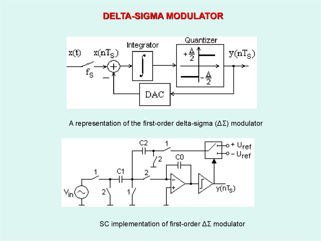
DELTA-SIGMA MODULATORA representation of the first-order delta-sigma (ΔΣ) modulator
SC implementation of first-order ΔΣ modulator
35. SIMULATION PROGRAMS OVERVIEW
ProgramLinear imperfections
Analysis in Analysis in Thermal
Analysis approach
Non-linear
time
frequency
noise
Switch
OpA
(method)
properties
domain
domain analysis resistance bandwidth
presents circuits as a
set of macroblocks
TOSCA described in terms of
internal state variables
presents circuits as a
AWEswit low order dominant
pole model
ASIDES
ZSIM
+
+
+
+
+
+
+
+
+
+
+
+
*
+
+
+
presents circuits as a
set of macroblocks
described in terms of
internal state variables
+
tableau method
+
performs transient MNA
SWITCAP2 based analysis for
linear circuits
formulates a set of
SDSIM finite difference
equations of the circuit
formulates set of the
SCNAP5 difference equation by
using MNA
+
+
+
36.
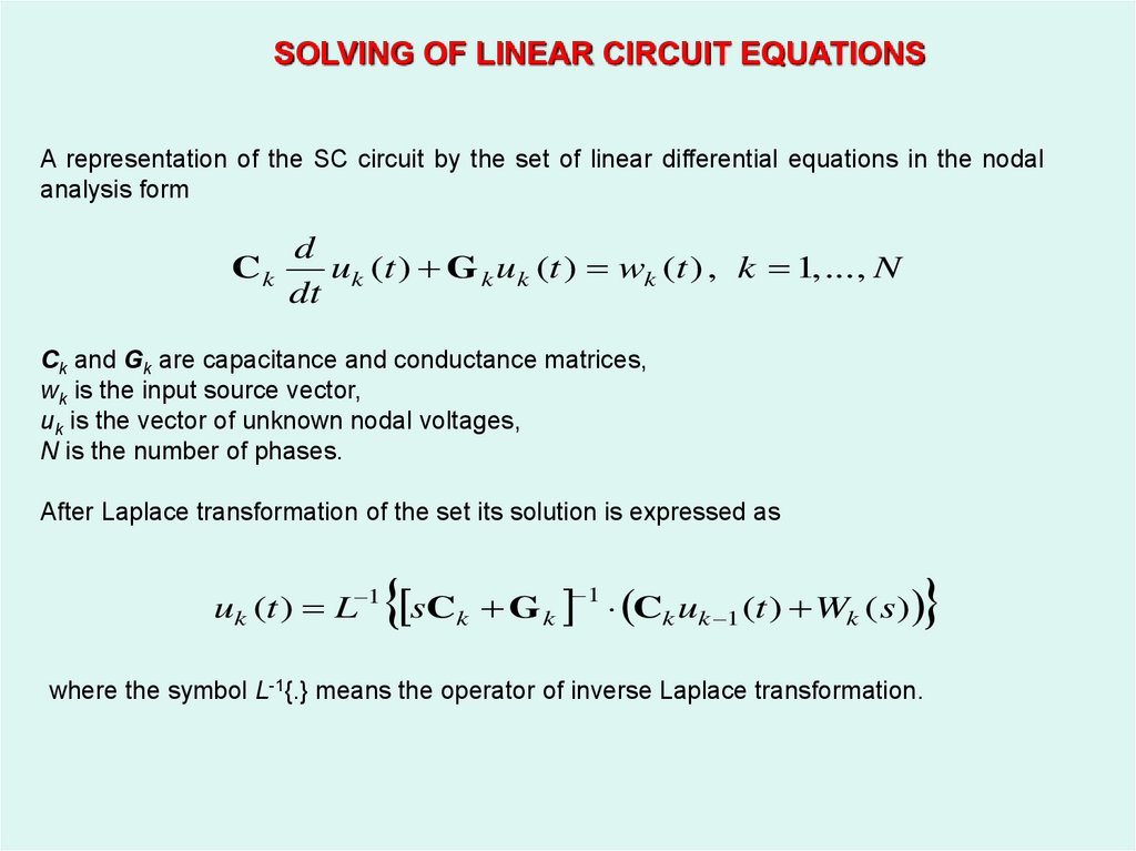
SOLVING OF LINEAR CIRCUIT EQUATIONSA representation of the SC circuit by the set of linear differential equations in the nodal
analysis form
Ck
d
uk (t ) G k u k (t ) wk (t ) , k 1, ... , N
dt
Ck and Gk are capacitance and conductance matrices,
wk is the input source vector,
uk is the vector of unknown nodal voltages,
N is the number of phases.
After Laplace transformation of the set its solution is expressed as
uk (t ) L 1 sCk G k
1
Ck uk 1 (t ) Wk ( s)
where the symbol L-1{.} means the operator of inverse Laplace transformation.
37. SOLVING OF NONLINEAR CIRCUIT EQUATIONS
A representation of the SC circuit by the set of nonlinear differential equations in the nodalanalysis form
d
C k u k t G k u k t wk t
dt
i
d
f u k t ,
u k t ,
i
dt
where f(·) is a function describing nonlinear properties of elements.
The circuit node variable vector using a truncated Volterra series expansion is expressed by
uk t u1k t1 u2 k t1 , t 2 u3k t1 , t 2 , t3
t1 t
t2 t
t3 t
For analysis of the second and the third harmonics the excitation vectors are presented in
general form as
w2k t f 2 u1k t ,
w3k t f 3 u1k t , u2k t1, t2 .
38. A. Capacitance nonlinearities
Nonlinear properties of the each parasitic drain-bulk and source-bulk capacitors of MOStransistors as switches are approximated by polynomial expression
c u t c0 a1 u t1 a2 u t1 2
The nonlinear capacitance matrix is rewritten as
C u t C0 C1 u1k t1 C2 u1k t1 u1k t1
where expression "u∙u" means multiplication of corresponding elements of the vectors .
The nodal analysis model of SC circuit can be rewritten as
C0k
d
d
u 2k t1 , t 2 G k u 2k t1 , t 2 C1k u1k t1 u1k t 2 ,
dt
dt
39.
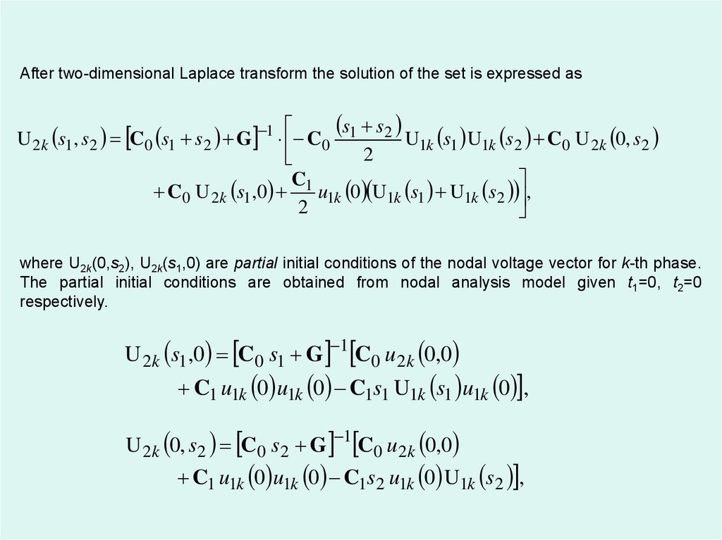
After two-dimensional Laplace transform the solution of the set is expressed ass s
U 2k s1 , s2 C0 s1 s2 G 1 C0 1 2 U1k s1 U1k s2 C0 U 2k 0, s2
2
C
C0 U 2k s1 ,0 1 u1k 0 U1k s1 U1k s2 ,
2
where U2k(0,s2), U2k(s1,0) are partial initial conditions of the nodal voltage vector for k-th phase.
The partial initial conditions are obtained from nodal analysis model given t1=0, t2=0
respectively.
U 2k s1 ,0 C0 s1 G 1 C0 u 2k 0,0
C1 u1k 0 u1k 0 C1s1 U1k s1 u1k 0 ,
U 2k 0, s2 C0 s2 G 1 C0 u 2k 0,0
C1 u1k 0 u1k 0 C1s2 u1k 0 U1k s2 ,
40. B. Active elements nonlinearities
The nonlinear DC characteristic of balanced amplifier can be approximated as followingpolynomial expression
u out t 0 uin t 3 uin t 3
Taking into account only the third order harmonic the nodal voltage vector can be expressed by
u k t u1k t1 u3k t1 , t 2 , t3 ,
The nodal analysis model of SC circuit can be rewritten as
Ck
d
u3k t1 , t 2 , t3 G k u3k t1 , t 2 , t3 G 3k u3k t1 , t 2 , t3 u3k t1 , t 2 , t3 u3k t1 , t 2 , t3 ,
dt
where G3k is conductance matrix of coefficients corresponding to nonlinear items in
polynomial expression describing active elements.
After three-dimensional Laplace transform the solution of the set is expressed as
U3k s1, s2 , s3 C s1 s2 s3 G 1 C R s1, s2 , s3 G 3k U1k s1 U1k s2 U1k s3 ,
where
R s1, s2 , s3 U3k 0, s2 , s3 U3k s1,0, s3 U3k s1, s2 ,0 .
41.
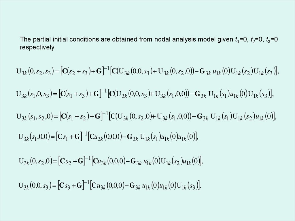
The partial initial conditions are obtained from nodal analysis model given t1=0, t2=0, t3=0respectively.
U3k 0, s2 , s3 C s2 s3 G 1 C U3k 0,0, s3 U3k 0, s2 ,0 G 3k u1k 0 U1k s2 U1k s3 ,
U3k s1,0, s3 C s1 s3 G 1 C U3k 0,0, s3 U3k s1,0,0 G 3k U1k s1 u1k 0 U1k s3 ,
U3k s1, s2 ,0 C s1 s2 G 1 C U3k 0, s2 ,0 U3k s1,0,0 G 3k U1k s1 U1k s2 u1k 0 ,
U3k s1,0,0 C s1 G 1 Cu3k 0,0,0 G 3k U1k s1 u1k 0 u1k 0 ,
U3k 0, s2 ,0 C s2 G 1 Cu3k 0,0,0 G 3k u1k 0 U1k s2 u1k 0 ,
U3k 0,0, s3 C s3 G 1 C u3k 0,0,0 G 3k u1k 0 u1k 0 U1k s3 .
42. Implementation of second-order ΔΣ modulator
SIMULATION EXAMPLEImplementation of second-order ΔΣ modulator
The equivalent circuit of the second-order ΔΣ modulator SC part in the first phase
43.
SIMULATION EXAMPLEline 1 – results of behavioral simulation using Simulink,
line 2 – gon=1 1/Ohm, ideal OpA,
line 3 – gon=1 1/Ohm, ideal OpA, sampling jitter with deviation of 0.05·10-6 sec,
line 4 – gon=1e-4 1/Ohm, GBW=200kHz).
44. Simulation results of second-order ΔΣ modulator for stray capacitor nonlinearities
45. Classification of Integrated Circuits
• ASIC – ApplicationSpecific IC
• MPIC – Mask
Programmed IC
• UPIC – User
Programmable IC
– FPGA – Field
Programmable Gate Array
– FPTA – Field
Programmable Transistor
Array
– FPAA – Field
Programmable Analog
Array
46. Typical FPAA Block Diagram
• Input/Output Blocks – ForAntialiasing and
Smoothing purposes
• CAB (Configurable
Analog Block ) – For
Analog Function
implementation
• Interconnection Network
– provides Internal
Connection between
CABs and I/O blocks
47. Main FPAA Vendors
Anadigm – specialized on switched capacitor ICs
Motorola – specialized on switched capacitor ICs
Zetex – specialized on continuous time ICs
Lattice semiconductor – specialized on
continuous time ICs
48.
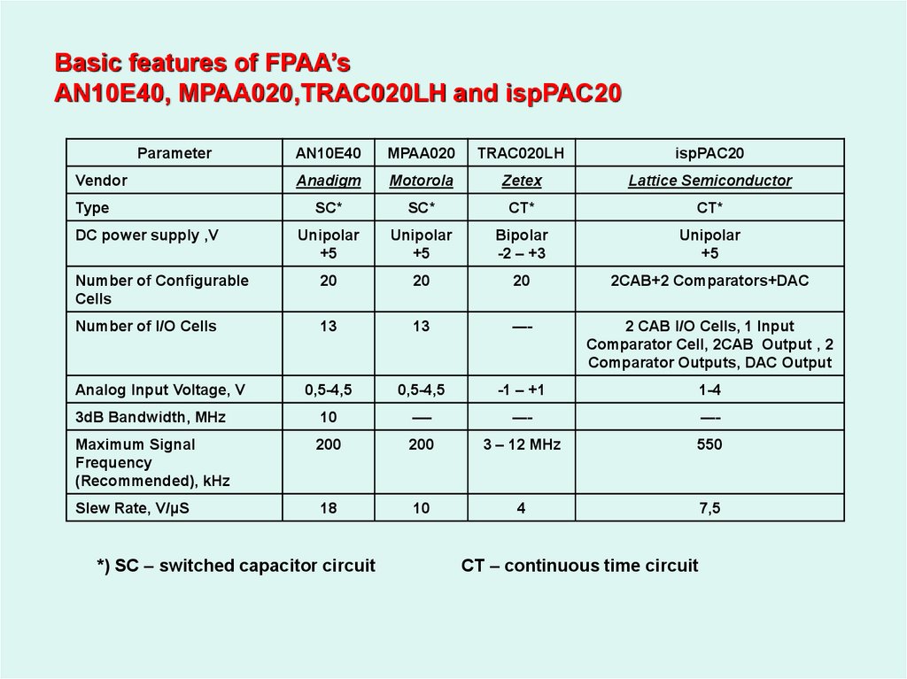
Basic features of FPAA’sAN10E40, MPAA020,TRAC020LH and ispPAC20
Parameter
AN10E40
MPAA020
TRAC020LH
ispPAC20
Anadigm
Motorola
Zetex
Lattice Semiconductor
SC*
SC*
CT*
CT*
Unipolar
+5
Unipolar
+5
Bipolar
-2 – +3
Unipolar
+5
Number of Configurable
Cells
20
20
20
2CAB+2 Comparators+DAC
Number of I/O Cells
13
13
----
2 CAB I/O Cells, 1 Input
Comparator Cell, 2CAB Output , 2
Comparator Outputs, DAC Output
0,5-4,5
0,5-4,5
-1 – +1
1-4
3dB Bandwidth, MHz
10
----
----
----
Maximum Signal
Frequency
(Recommended), kHz
200
200
3 – 12 MHz
550
Slew Rate, V/μS
18
10
4
7,5
Vendor
Type
DC power supply ,V
Analog Input Voltage, V
*) SC – switched capacitor circuit
CT – continuous time circuit
49. Anadigm’s CAB Block Diagram
50.
FPAA implementation of Delta-Sigma Modulator (Anadigm Designer Software)Integrator
First-order
DAC
Comparator
Adder - Subtractor block
Sample-and-Hold
51. Computer Simulation
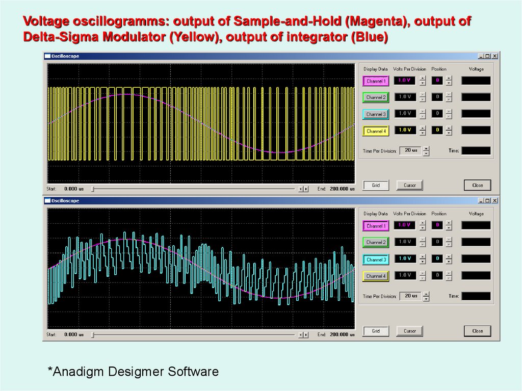
Initial Conditions
Clock Frequency 1MHz
Test signal Frequency 5kHz
Amplitude of test signal 2V
Integration Constant of Integrator 10e6/s
52.
Voltage oscillogramms: output of Sample-and-Hold (Magenta), output ofDelta-Sigma Modulator (Yellow), output of integrator (Blue)
*Anadigm Desigmer Software
53.
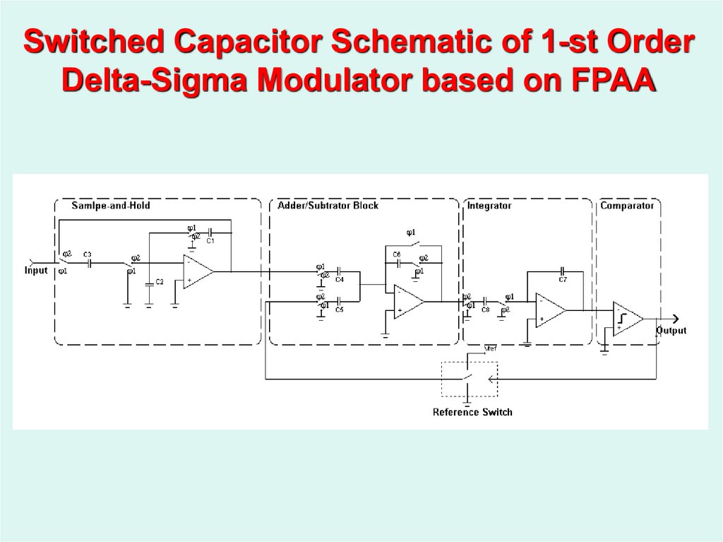
Switched Capacitor Schematic of 1-st OrderDelta-Sigma Modulator based on FPAA
54.
Measuring Scheme55.
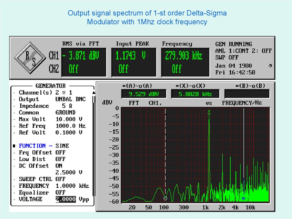
Output signal spectrum of 1-st order Delta-SigmaModulator with 1Mhz clock frequency
56.
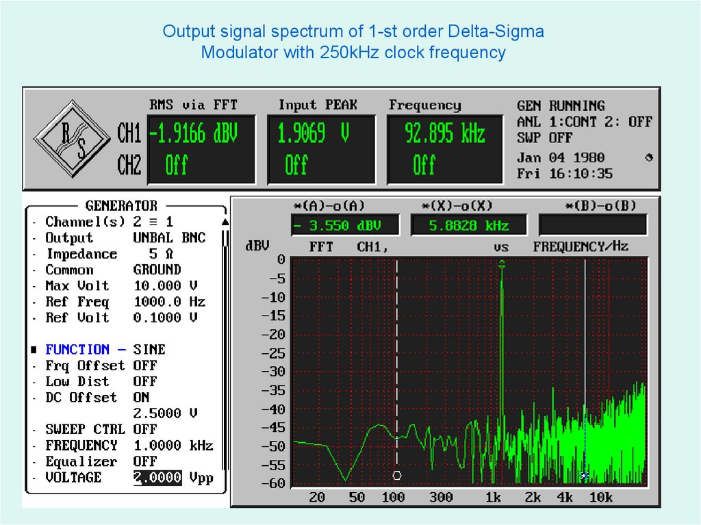
Output signal spectrum of 1-st order Delta-SigmaModulator with 250kHz clock frequency
57.
58. Conclusions
1.Proposed approaches are perspective and can be used for theCMOS design of selective circuits for wireless communication
systems.
2.Characteristics of the synthesized filters correspond to practical
requirements.
3.Main advantages of the circuits are their low supply voltage and
power consumption as well as their small sizes and good
compatibility with CMOS technology.
59. CONCLUSIONS
4. Simulation program has been proposed for analysis of oversampledswitched-capacitor Delta-Sigma modulator.
5. The developed program is based on direct circuit response
calculation using nodal approach with matrix presentation of circuits
in the frequency domain and Volterra series method.
6. The program is written in MATLAB and allows
– analysis of switched-capacitor circuit taking into account nonideal imperfections including limited switch resistances and gainbandwidth product of active devices.
– analysis of switched-capacitor circuit taking into account
nonlinear parasitic capacitance of switches and active elements
dynamic limitations
60. CONCLUSIONS
• Delta-Sigma modulator has been realized on a basis ofFPAA Anadigm AN10E40;
• For the proposed design the Dynamic Range is not more
than 40 dB and the Frequency Range is about 20 kHz;
• The limiting factors:
– OSR not more than 100. It depends on FPAA properties;
– Properties of comparator;
– Possibly, schematic of the integrators as well.
61. References
[1] D.V.Morozov and A.S.Korotkov, “A realization of low-distortion CMOS
transconductance amplifier;” IEEE Trans. Circuits Syst.-I, vol.48, pp.1138-1141,
Sept. 2001.
[2] A.S.Korotkov, D.V.Morozov, and R.Unbehauen, “Low-voltage continuous
time filter based on a CMOS transconductor with enhanced linearity,” Int. J.
Electronics and Comm. (AEÜ), vol.56, no.6, pp.416- 420, Dec. 2002.
[3] A.S.Korotkov, D.V.Morozov, H.Hauer, and R.Unbehauen, “A 2.5-V, 0.35 um
CMOS transconductance-capacitor filter with enhanced linearity,” In Proc.
MWSCAS’02, Tulsa, USA, vol.3, pp.141- 144, Aug. 2002.
[4] A.A.Tutyshkin, A.S.Korotkov, “Current conveyor based switched-capacitor
integrator with reduced parasitic sensitivity,” in Proc 1st IEEE ICCSC’02,
St.Petersburg, Russia, pp.78- 81, June 2002.
[5] A.S.Korotkov, D.V.Morozov, A.A.Tutyshkin, H.Hauer and R.Unbehauen,
“Design of a CMOS high frequency current conveyor based switched-capacitor
filter with low power consumption,” in Proc. MWSCAS’03, Cairo, Dec. 2003.
THANK YOU