


 Маркетинг
Похожие презентации:


")

Semishare. Introduction
1.
SEMISHAREIntroduction
Advanced wafer prober manufacturer
2.
ABOUTSEMISHARE is committed to providing its customers with advanced level wafer prober equipment and
semiconductor test and measurement solutions. At present, we have customers in more than 1000
well-known institutions and enterprises, including scientific research institutions, the chip design
companies, fabs, sealing test factories and panel manufacturing industry, etc. As China's semiconductor
industry is on the rise, SEMISHARE already have many successful Projects and technology development
experiences as the world's leading wafer prober manufacturers, benchmarking in semiconductor test
and measurement field.
3.
Innovation Drives DevelopmentStart
2010.11
2012-2016
2011.3
launched a low-temperature
vacuum probe station
2014.6
Wafer Test HALL test system
released
2015.4.
In China, the Flex series was
launched for TFT-LCD/OLED
2015-10
The first inline CVD laser
repair machine was launched
in China
2015-2017
2018-2020
2016.4.
Become Integration Partner of
Keithley, Keysight System
2018.5
Release of semi-automatic
probe stations
2016.6
Harbin Institute of Technology
jointly built the National
Science Project
2019.7
Successfully obtained the first
round of investment from
high-tech investment
2019.10
Obtained orders for mass
production lines of domestic
semiconductor leading
enterprises
2021- To date
21 years of Walden
International investment
2022.5
Get a fully automated wafer
probe station sales order
2022.8
Won the title of national
specialized,
special and new "little giant"
enterprise
4.
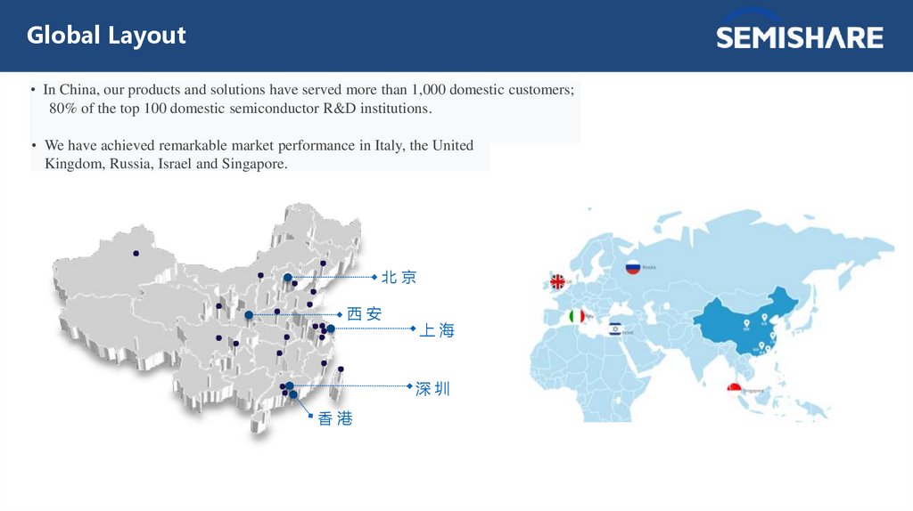
Global Layout• In China, our products and solutions have served more than 1,000 domestic customers;
80% of the top 100 domestic semiconductor R&D institutions.
• We have achieved remarkable market performance in Italy, the United
Kingdom, Russia, Israel and Singapore.
北京
西安
上海
深圳
香港
5.
Our PartnersIntegrated Circuit Design/Manufacturing/Packaging and Testing Enterprises
6.
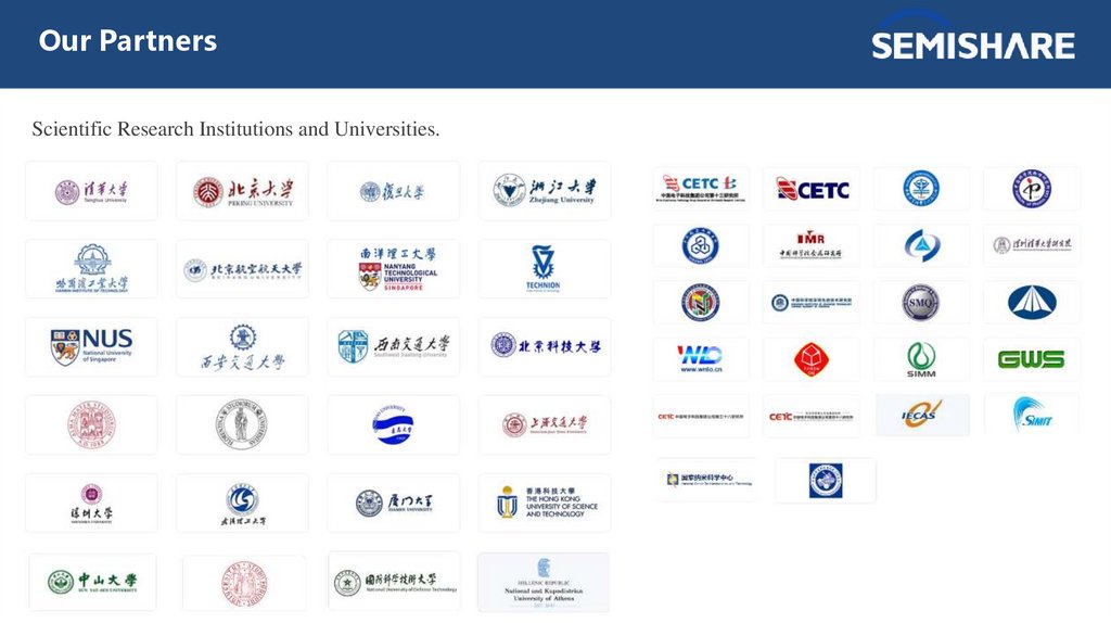
Our PartnersScientific Research Institutions and Universities.
7.
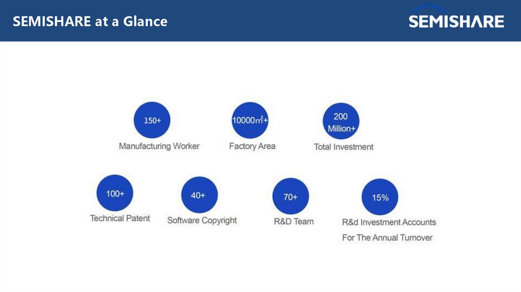
SEMISHARE at a Glance8.
Customers9.
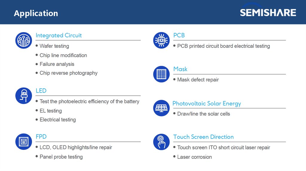
Application10.
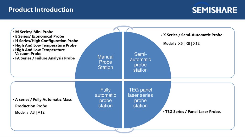
Product Introduction• M Series/ Mini Probe
• E Series/ Economical Probe
• H Series/High Configuration Probe
• High And Low Temperature Probe
• High And Low Temperature
Vacuum Probe
• FA Series / Failure Analysis Probe
• A series / Fully Automatic Mass
Production Probe
Model A8 | A12
• X Series / Semi-Automatic Probe
Model X6 | X8 | X12
Manual
Probe
Station
Semiautomatic
probe
station
Fully
automatic
probe
station
TEG panel
laser series
probe
station
• TEG Series / Panel Laser Probe。
11.
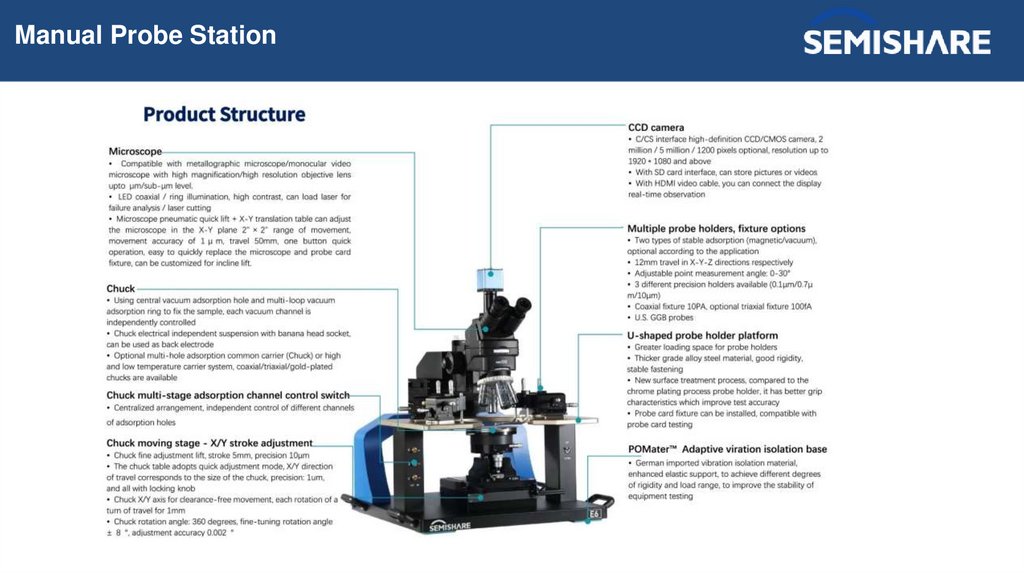
Manual Probe Station12.
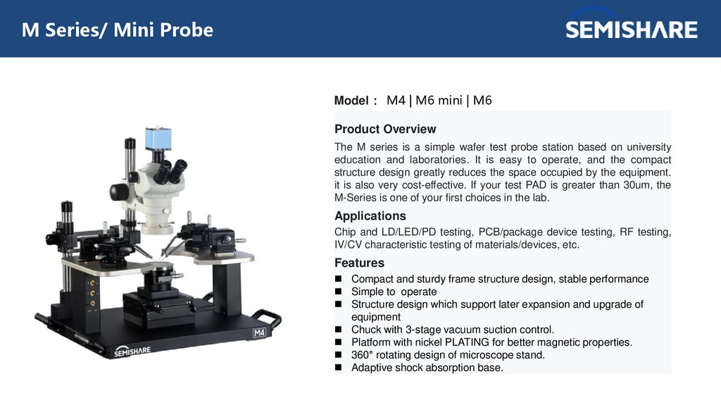
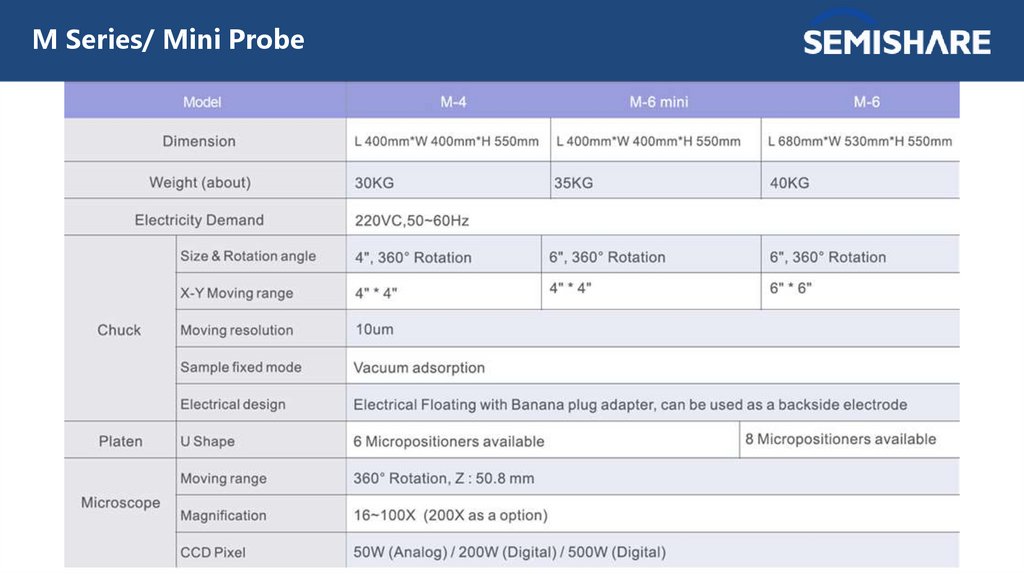
M Series/ Mini ProbeModel M4 | M6 mini | M6
Product Overview
The M series is a simple wafer test probe station based on university
education and laboratories. It is easy to operate, and the compact
structure design greatly reduces the space occupied by the equipment.
it is also very cost-effective. If your test PAD is greater than 30um, the
M-Series is one of your first choices in the lab.
Applications
Chip and LD/LED/PD testing, PCB/package device testing, RF testing,
IV/CV characteristic testing of materials/devices, etc.
Features
Compact and sturdy frame structure design, stable performance
Simple to operate
Structure design which support later expansion and upgrade of
equipment
Chuck with 3-stage vacuum suction control.
Platform with nickel PLATING for better magnetic properties.
360° rotating design of microscope stand.
Adaptive shock absorption base.
13.
M Series/ Mini Probe14.
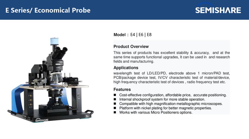
E Series/ Economical ProbeModel E4 | E6 | E8
Product Overview
This series of products has excellent stability & accuracy, and at the
same time supports functional upgrades, It can be used in and research
fields and manufacturing.
Applications
wavelength test of LD/LED/PD, electrode above 1 micron/PAD test,
PCB/package device test, IV/CV characteristic test of material/device,
high frequency characteristic test of devices , radio frequency test etc.
Features
Cost-effective configuration, affordable price, accurate positioning.
Internal shockproof system for more stable operation.
Compatible with high magnification metallographic microscopes.
Platform with nickel plating for better magnetic properties.
Works with various Micro Positioners options.
15.
E Series/ Economical Probe16.
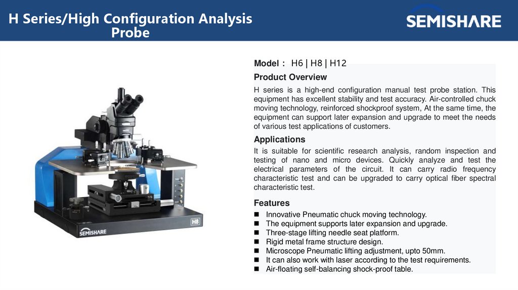
H Series/High Configuration AnalysisProbe
Model H6 | H8 | H12
Product Overview
H series is a high-end configuration manual test probe station. This
equipment has excellent stability and test accuracy. Air-controlled chuck
moving technology, reinforced shockproof system, At the same time, the
equipment can support later expansion and upgrade to meet the needs
of various test applications of customers.
Applications
It is suitable for scientific research analysis, random inspection and
testing of nano and micro devices. Quickly analyze and test the
electrical parameters of the circuit. It can carry radio frequency
characteristic test and can be upgraded to carry optical fiber spectral
characteristic test.
Features
Innovative Pneumatic chuck moving technology.
The equipment supports later expansion and upgrade.
Three-stage lifting needle seat platform.
Rigid metal frame structure design.
Microscope Pneumatic lifting adjustment, upto 50mm.
It can also work with laser according to the test requirements.
Air-floating self-balancing shock-proof table.
17.
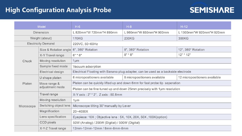
High Configuration Analysis Probe18.
Manual Probe stations comparison19.
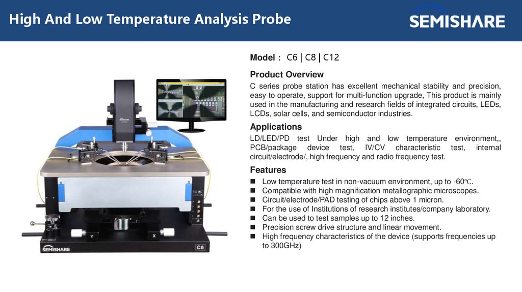
High And Low Temperature Analysis ProbeModel C6 | C8 | C12
Product Overview
C series probe station has excellent mechanical stability and precision,
easy to operate, support for multi-function upgrade, This product is mainly
used in the manufacturing and research fields of integrated circuits, LEDs,
LCDs, solar cells, and semiconductor industries.
Applications
LD/LED/PD test Under high and low temperature environment,,
PCB/package device test, IV/CV characteristic test, internal
circuit/electrode/, high frequency and radio frequency test.
Features
Low temperature test in non-vacuum environment, up to -60℃.
Compatible with high magnification metallographic microscopes.
Circuit/electrode/PAD testing of chips above 1 micron.
For the use of Institutions of research institutes/company laboratory.
Can be used to test samples up to 12 inches.
Precision screw drive structure and linear movement.
High frequency characteristics of the device (supports frequencies up
to 300GHz)
20.
High And Low Temperature Analysis Probe21.
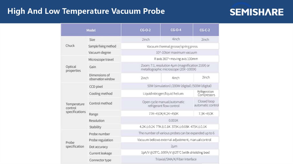
High And Low Temperature Vacuum ProbeModel CG-O-2 | CG-O-4 | CG-C-2
Product Overview
This series is developed by SEMISHARE with the collaboration of
Harbin Institute of Technology and China Aerospace Science and
Technology Group. It is mainly used in integrated circuits, LEDs,
Manufacturing and research fields in LCD, solar cells and other industries.
Applications
Chip test in high and low temperature vacuum environment, LD/LED/PD
test, optical fiber spectral characteristic test, IV/CV characteristic test of
material/device, Hall test, electromagnetic transport characteristic, high
frequency characteristic test, etc.
Features
High and low temperature test in vacuum environment (4.2K~450K).
High frequency characteristics of the device (supports up to 67GHz
frequency).
Support optical fiber spectral characteristics test.
Anti-radiation screen design, better uniformity of sample temperature.
Compatible with high magnification metallographic microscopes.
Automatic flow control of refrigeration fluid.
22.
High And Low Temperature Vacuum Probe23.
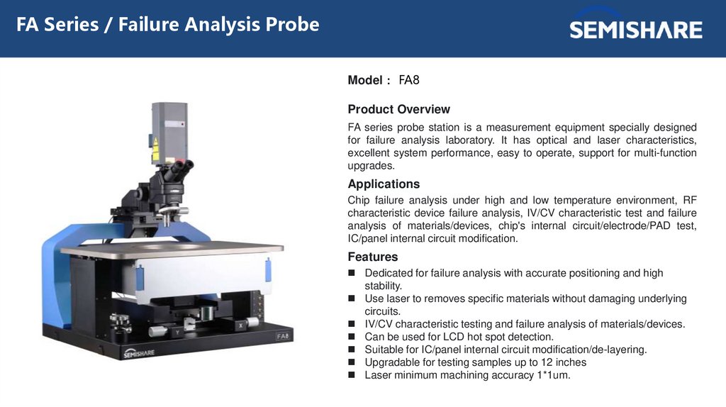
FA Series / Failure Analysis ProbeModel FA8
Product Overview
FA series probe station is a measurement equipment specially designed
for failure analysis laboratory. It has optical and laser characteristics,
excellent system performance, easy to operate, support for multi-function
upgrades.
Applications
Chip failure analysis under high and low temperature environment, RF
characteristic device failure analysis, IV/CV characteristic test and failure
analysis of materials/devices, chip's internal circuit/electrode/PAD test,
IC/panel internal circuit modification.
Features
Dedicated for failure analysis with accurate positioning and high
stability.
Use laser to removes specific materials without damaging underlying
circuits.
IV/CV characteristic testing and failure analysis of materials/devices.
Can be used for LCD hot spot detection.
Suitable for IC/panel internal circuit modification/de-layering.
Upgradable for testing samples up to 12 inches
Laser minimum machining accuracy 1*1um.
24.
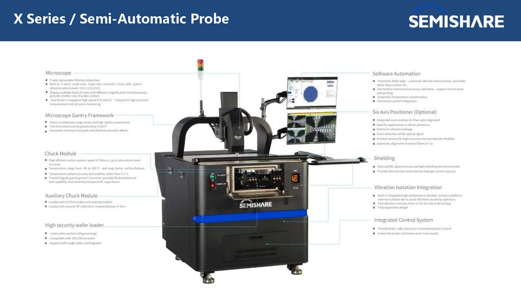
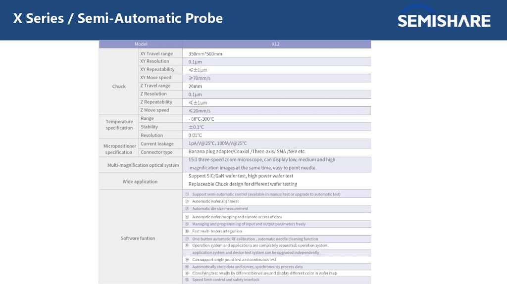
X Series / Semi-Automatic ProbeModel X6 | X8 | X12
Product Overview
X series is a semi-automatic probe station that integrates electrical, light
wave, microwave and other testing functions. It can perform On-chip
detection of wafers, MEMS, optoelectronic devices and other integrated
circuits, LEDs, LCDs, solar cells, etc. It can be loaded with temperature
control systems to meet customers' various requirements in high and low
temperature environments.
Applications
I-V, C-V, optical signal, characteristic analysis, RF test, high-power test.
Features
The running speed is over 70mm/s with High test accuracy, operation
efficiency and system stability.
Multi-magnification optical display system, high-precision measurement
and dynamic monitoring
Leading internal anti-vibration system device with more stable operation.
Integrated control system, quick access to instrument testing.
Software automated testing with precise calibration of mechanical
accuracy.
25.
X Series / Semi-Automatic Probe26.
X Series / Semi-Automatic Probe27.
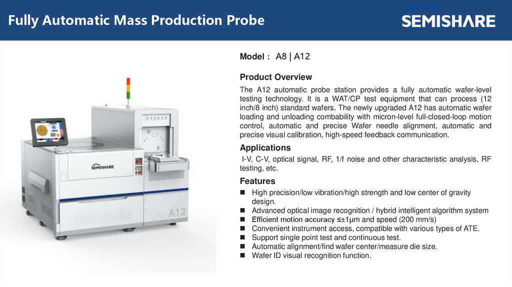
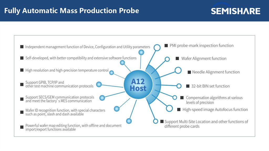
Fully Automatic Mass Production ProbeModel A8 | A12
Product Overview
The A12 automatic probe station provides a fully automatic wafer-level
testing technology. It is a WAT/CP test equipment that can process (12
inch/8 inch) standard wafers. The newly upgraded A12 has automatic wafer
loading and unloading combability with micron-level full-closed-loop motion
control, automatic and precise Wafer needle alignment, automatic and
precise visual calibration, high-speed feedback communication.
Applications
I-V, C-V, optical signal, RF, 1/f noise and other characteristic analysis, RF
testing, etc.
Features
High precision/low vibration/high strength and low center of gravity
design.
Advanced optical image recognition / hybrid intelligent algorithm system
Efficient motion accuracy ≤±1μm and speed (200 mm/s)
Convenient instrument access, compatible with various types of ATE.
Support single point test and continuous test.
Automatic alignment/find wafer center/measure die size.
Wafer ID visual recognition function.
28.
Fully Automatic Mass Production Probe29.
Fully Automatic Mass Production Probe30.
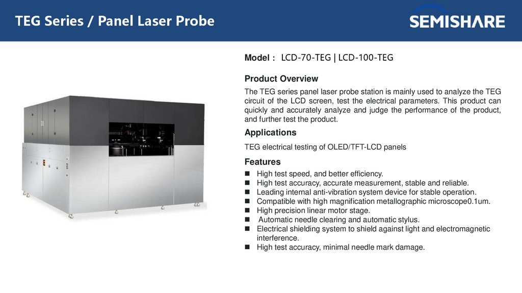
TEG Series / Panel Laser ProbeModel LCD-70-TEG | LCD-100-TEG
Product Overview
The TEG series panel laser probe station is mainly used to analyze the TEG
circuit of the LCD screen, test the electrical parameters. This product can
quickly and accurately analyze and judge the performance of the product,
and further test the product.
Applications
TEG electrical testing of OLED/TFT-LCD panels
Features
High test speed, and better efficiency.
High test accuracy, accurate measurement, stable and reliable.
Leading internal anti-vibration system device for stable operation.
Compatible with high magnification metallographic microscope0.1um.
High precision linear motor stage.
Automatic needle clearing and automatic stylus.
Electrical shielding system to shield against light and electromagnetic
interference.
High test accuracy, minimal needle mark damage.
31.
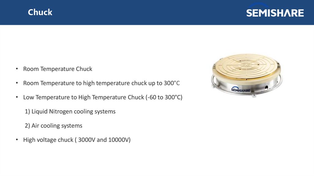
Chuck• Room Temperature Chuck
• Room Temperature to high temperature chuck up to 300°C
• Low Temperature to High Temperature Chuck (-60 to 300°C)
1) Liquid Nitrogen cooling systems
2) Air cooling systems
• High voltage chuck ( 3000V and 10000V)
32.
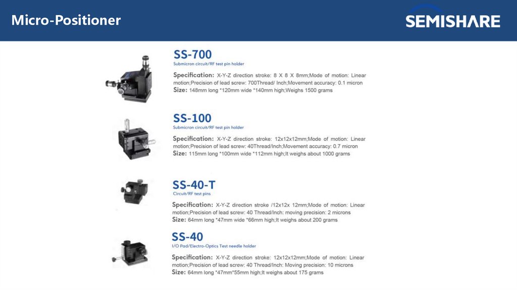
Micro-Positioner33.
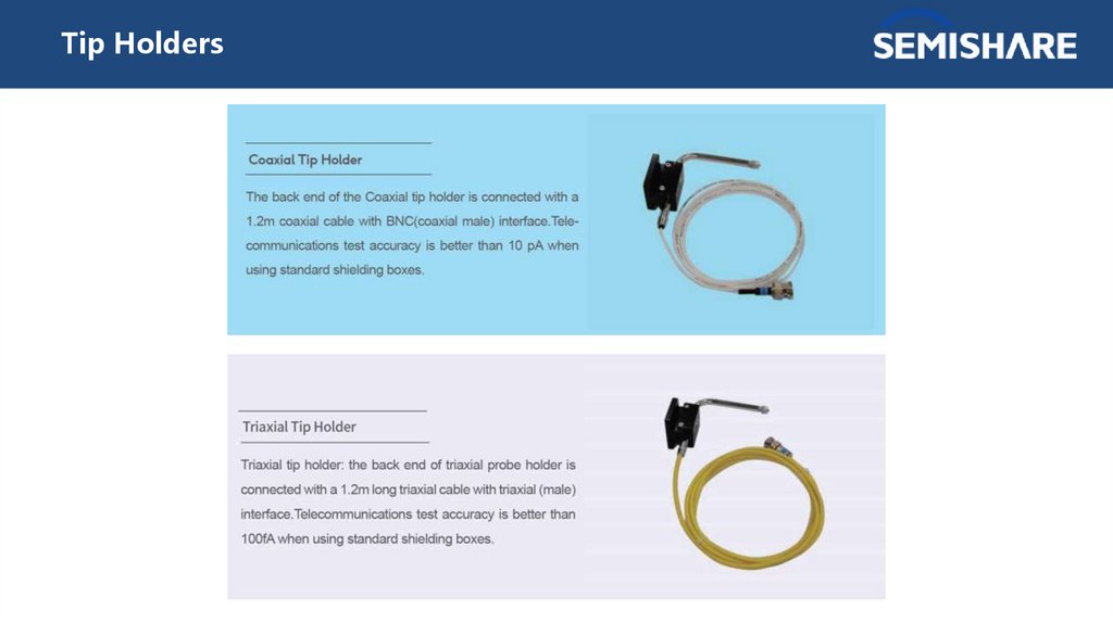
Tip Holders34.
Questions regarding A12 and A8:1. Could you please send us quote for A8, because we have project for wafers 100-150 mm.
Yes, we will send you our standard version quotes of A8 after the meeting. If any special requirements, we can discuss
one by one.
35.
2. Option of Xandeх marker – could it be installed/used only with A12 or it is also can be used with A8? What is the pricefor it?
Yes, the Xandex marker can be used with our A8&A12, but if you have any specific model, you can share that, and we will
discuss the feasibility with our technical department.
36.
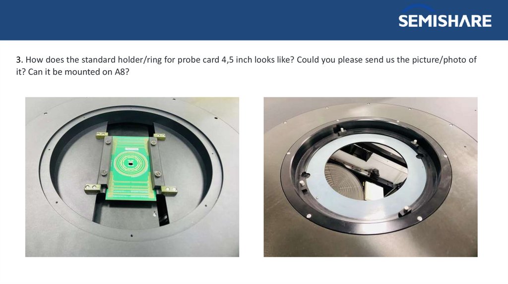
3. How does the standard holder/ring for probe card 4,5 inch looks like? Could you please send us the picture/photo ofit? Can it be mounted on A8?
37.
4, Our customers have a lot of probe cards of Accretech standards (see attached photos). Can you manufacture theholder/ring for such probe cards? Such holders/rings we usually ordered from Esmo. Please note that there are probe
cards with a cross - only for connecting the cable.
Yes, we can manufacture according to the provided design and drawings
5. Is the A12 station equipped with the option of automatic change of sample cards (Accretech standard).
Yes. Full automatic prober can automatic change of sample cards.
6. Attached is a photo with examples of our work with our customers (there is a photo of a cable connection with probe
cards, there is a photo of a hard connection).
OK.
7. Based on our experience, we inform you that for the manufacture of a ring (fastening) for sample cards, we took the
dimensions of the top plate from Accretech, and ESMO made the necessary docking for us.
38.
Questions regarding X12, C8 and FA-8-SC:-Delivery time and price for X12, C8 and FA-8-SC.
The lead time is around 12~16 weeks for X12, C8 and FA series, the price depends on the configuration, the configuration
depends on customer’s requirments. We can discuss one by one.
-What kind of laser is installed/mounted on the FA-8-SC. Who is the manufacturer of the laser?
Following are two options that we have for laser
39.
-How is the chuck temperature regulated in these probes.
-
We have temperature controllers according to the type of chucks. They control the heating systems and cooling fluids
(Air, Liquid Nitrogen, and Liquid He)
40.
Is it possible to supply X8 i.e. 200mmYes X8 comes with 8 inch chuck option.
41.
THANKSAdvanced wafer prober manufacturer