


 Программное обеспечение
Похожие презентации:


")


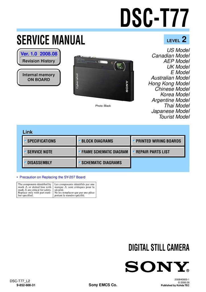
DSC-T77. Service manual
1.
DSC-T77SERVICE MANUAL
LEVEL
Ver. 1.0 2008.08
Revision History
Internal memory
ON BOARD
Photo: Black
2
US Model
Canadian Model
AEP Model
UK Model
E Model
Australian Model
Hong Kong Model
Chinese Model
Korea Model
Argentine Model
Thai Model
Japanese Model
Tourist Model
Link
SPECIFICATIONS
BLOCK DIAGRAMS
PRINTED WIRING BOARDS
SERVICE NOTE
FRAME SCHEMATIC DIAGRAM
REPAIR PARTS LIST
DISASSEMBLY
SCHEMATIC DIAGRAMS
• Precaution on Replacing the SY-207 Board
The components identified by
mark 0 or dotted line with
mark 0 are critical for safety.
Replace only with part number specified.
Les composants identifiés par une
marque 0 sont critiques pour la
sécurité.
Ne les remplacer que par une pièce
portant le numéro spécifié.
DIGITAL STILL CAMERA
DSC-T77_L2
9-852-608-31
Sony EMCS Co.
2008H0800-1
© 2008.08
Published by Kohda TEC
2.
SPECIFICATIONSCamera
[System]
Image device: 7.7 mm (1/2.3 type) color CCD,
Primary color filter
Total pixel number of camera: Approx. 10.3
Megapixels
Effective pixel number of camera: Approx. 10.1
Megapixels
Lens: Carl Zeiss Vario-Tessar 4× zoom lens
f = 6.18 – 24.7 mm (35 – 140 mm (35 mm
film equivalent))
F3.5 (W) – F4.6 (T)
Exposure control: Automatic exposure, Scene
Selection (11 modes)
White balance: Automatic, Daylight, Cloudy,
Fluorescent 1,2,3, Incandescent, Flash
Underwater White Balance: Auto, Underwater
1,2, Flash
File format (DCF compliant):
Still images: Exif Ver. 2.21 JPEG compliant,
DPOF compatible
Movies: MPEG1 compliant (Monaural)
Recording media: Internal Memory
(approx. 15 MB), “Memory Stick Duo”
Flash: Flash range (ISO sensitivity
(Recommended exposure Index) set to Auto):
Approx. 0.08 to 3.0 m (3 1/4 inches to
9 feet 10 1/8 inches) (W)/
approx. 0.5 to 2.4 m (1 feet 7 3/4 inches to
7 feet 10 1/2 inches) (T)
[Input and Output connectors]
BC-CSD battery charger
Multi connector:Video output
Audio output (Monaural)
USB communication
USB communication: Hi-Speed USB (USB 2.0
compliant)
Power requirements: AC 100 V to 240 V,
50/60 Hz, 2.2 W
Output voltage: DC 4.2 V, 0.33 A
Operating temperature: 0 to 40˚C (32 to 104˚F)
Storage temperature: -20 to +60˚C (-4 to +140˚F)
Dimensions: Approx. 62 × 24 × 91 mm (2 1/2 ×
31/32 × 3 5/8 inches) (W/H/D)
Mass: Approx. 75 g (2.7 oz)
[LCD screen]
LCD panel: Wide (16:9), 7.5 cm (3.0 type) TFT
drive
Total number of dots: 230 400 (960 × 240) dots
[Power, general]
Power: Rechargeable battery pack NP-BD1, 3.6 V
NP-FD1 (not supplied), 3.6 V
AC-LS5K AC Adaptor (not supplied), 4.2 V
Power consumption (during shooting): 1.1 W
Operating temperature: 0 to 40˚C (32 to 104˚F)
Storage temperature: -20 to +60˚C (-4 to +140˚F)
Dimensions: 93.6 × 57.2 × 15.0 mm (3 3/4 × 2 3/8
× 19/32 inches) (W/H/D, excluding
protrusions)
Mass (including NP-BD1 battery pack, paint pen
and strap etc.): Approx. 151 g (5.3 oz)
Microphone: Monaural
Speaker: Monaural
Exif Print: Compatible
PRINT Image Matching III: Compatible
PictBridge: Compatible
DSC-T77_L2
—2—
Rechargeable battery pack
NP-BD1
Used battery: Lithium-ion battery
Maximum voltage: DC 4.2 V
Nominal voltage: DC 3.6 V
Capacity: 2.4 Wh (680 mAh)
Design and specifications are subject to
change without notice.
3.
CAUTIONDanger of explosion if battery is incorrectly replaced.
Replace only with the same or equivalent type.
SAFETY-RELATED COMPONENT WARNING!!
COMPONENTS IDENTIFIED BY MARK 0 OR DOTTED LINE WITH
MARK 0 ON THE SCHEMATIC DIAGRAMS AND IN THE PARTS
LIST ARE CRITICAL TO SAFE OPERATION. REPLACE THESE
COMPONENTS WITH SONY PARTS WHOSE PART NUMBERS
APPEAR AS SHOWN IN THIS MANUAL OR IN SUPPLEMENTS
PUBLISHED BY SONY.
ATTENTION AU COMPOSANT AYANT RAPPORT
À LA SÉCURITÉ!
LES COMPOSANTS IDENTIFÉS PAR UNE MARQUE 0 SUR LES
DIAGRAMMES SCHÉMATIQUES ET LA LISTE DES PIÈCES SONT
CRITIQUES POUR LA SÉCURITÉ DE FONCTIONNEMENT. NE
REMPLACER CES COMPOSANTS QUE PAR DES PIÈSES SONY
DONT LES NUMÉROS SONT DONNÉS DANS CE MANUEL OU
DANS LES SUPPÉMENTS PUBLIÉS PAR SONY.
SAFETY CHECK-OUT
After correcting the original service problem, perform the following
safety checks before releasing the set to the customer.
1.
2.
3.
4.
5.
6.
Check the area of your repair for unsoldered or poorly-soldered
connections. Check the entire board surface for solder splashes
and bridges.
Check the interboard wiring to ensure that no wires are
"pinched" or contact high-wattage resistors.
Look for unauthorized replacement parts, particularly
transistors, that were installed during a previous repair. Point
them out to the customer and recommend their replacement.
Look for parts which, through functioning, show obvious signs
of deterioration. Point them out to the customer and
recommend their replacement.
Check the B+ voltage to see it is at the values specified.
Flexible Circuit Board Repairing
• Keep the temperature of the soldering iron around 270˚C
during repairing.
• Do not touch the soldering iron on the same conductor of the
circuit board (within 3 times).
• Be careful not to apply force on the conductor when soldering
or unsoldering.
Unleaded solder
Boards requiring use of unleaded solder are printed with the leadfree mark (LF) indicating the solder contains no lead.
(Caution: Some printed circuit boards may not come printed with
the lead free mark due to their particular size.)
: LEAD FREE MARK
Unleaded solder has the following characteristics.
• Unleaded solder melts at a temperature about 40°C higher than
ordinary solder.
Ordinary soldering irons can be used but the iron tip has to be
applied to the solder joint for a slightly longer time.
Soldering irons using a temperature regulator should be set to
about 350°C.
Caution: The printed pattern (copper foil) may peel away if the
heated tip is applied for too long, so be careful!
• Strong viscosity
Unleaded solder is more viscous (sticky, less prone to flow) than
ordinary solder so use caution not to let solder bridges occur such
as on IC pins, etc.
• Usable with ordinary solder
It is best to use only unleaded solder but unleaded solder may
also be added to ordinary solder.
DSC-T77_L2
—3—
4.
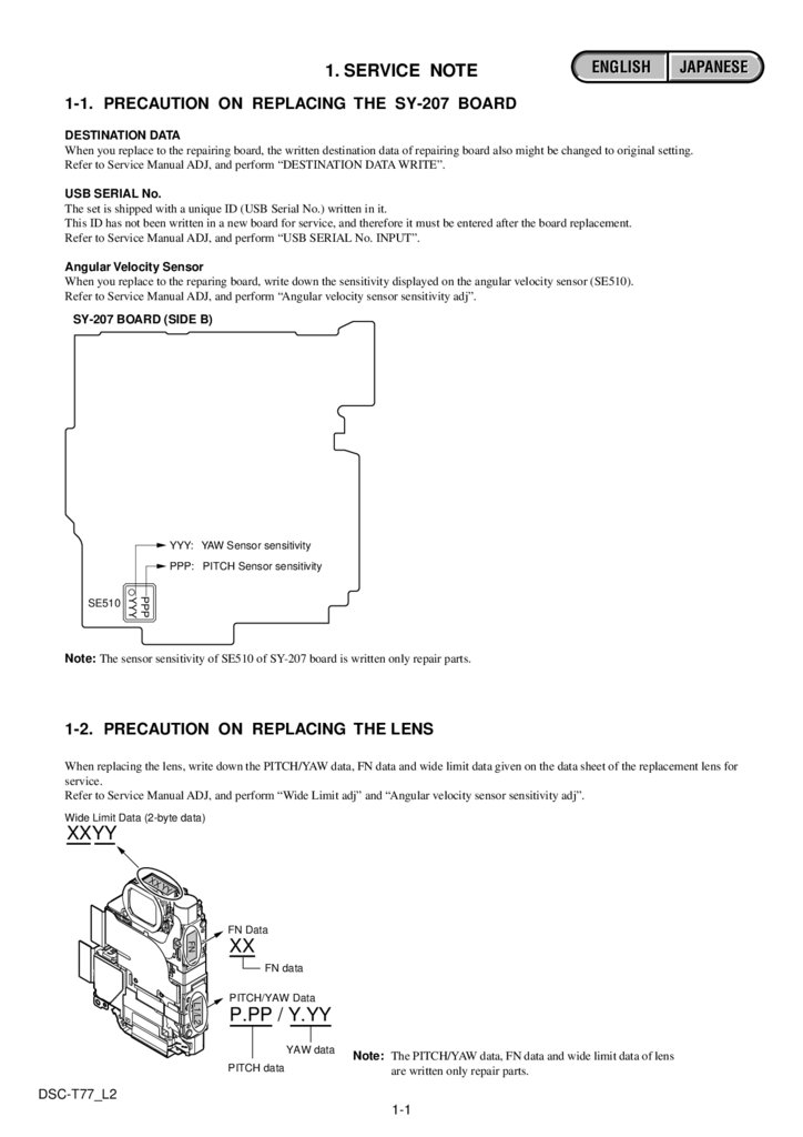
1. SERVICE NOTEENGLISH
JAPANESE
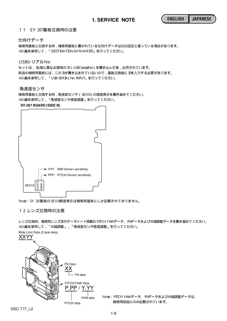
1-1. PRECAUTION ON REPLACING THE SY-207 BOARD
DESTINATION DATA
When you replace to the repairing board, the written destination data of repairing board also might be changed to original setting.
Refer to Service Manual ADJ, and perform “DESTINATION DATA WRITE”.
USB SERIAL No.
The set is shipped with a unique ID (USB Serial No.) written in it.
This ID has not been written in a new board for service, and therefore it must be entered after the board replacement.
Refer to Service Manual ADJ, and perform “USB SERIAL No. INPUT”.
Angular Velocity Sensor
When you replace to the reparing board, write down the sensitivity displayed on the angular velocity sensor (SE510).
Refer to Service Manual ADJ, and perform “Angular velocity sensor sensitivity adj”.
SY-207 BOARD (SIDE B)
YYY: YAW Sensor sensitivity
PPP: PITCH Sensor sensitivity
PPP
YYY
SE510
Note: The sensor sensitivity of SE510 of SY-207 board is written only repair parts.
1-2. PRECAUTION ON REPLACING THE LENS
When replacing the lens, write down the PITCH/YAW data, FN data and wide limit data given on the data sheet of the replacement lens for
service.
Refer to Service Manual ADJ, and perform “Wide Limit adj” and “Angular velocity sensor sensitivity adj”.
Wide Limit Data (2-byte data)
XXYY
XX
YY
FN Data
FN
XX
FN data
L 1 /L 2
PITCH/YAW Data
P.PP / Y.YY
YAW data
PITCH data
Note: The PITCH/YAW data, FN data and wide limit data of lens
are written only repair parts.
DSC-T77_L2
1-1
5.
ENGLISHJAPANESE
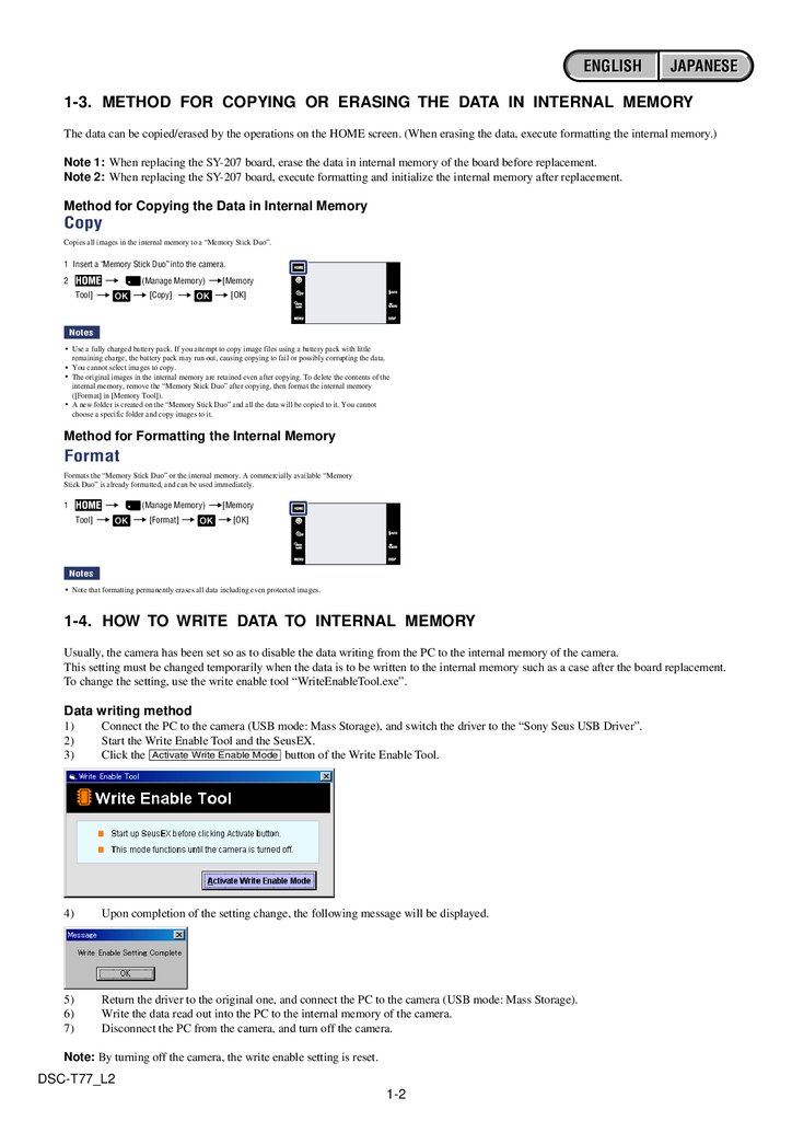
1-3. METHOD FOR COPYING OR ERASING THE DATA IN INTERNAL MEMORY
The data can be copied/erased by the operations on the HOME screen. (When erasing the data, execute formatting the internal memory.)
Note 1: When replacing the SY-207 board, erase the data in internal memory of the board before replacement.
Note 2: When replacing the SY-207 board, execute formatting and initialize the internal memory after replacement.
Method for Copying the Data in Internal Memory
Copy
Copies all images in the internal memory to a “Memory Stick Duo”.
1 Insert a “Memory Stick Duo” into the camera.
2
(Manage Memory)
Tool]
[Copy]
[Memory
[OK]
Notes
Use a fully charged battery pack. If you attempt to copy image files using a battery pack with little
remaining charge, the battery pack may run out, causing copying to fail or possibly corrupting the data.
You cannot select images to copy.
The original images in the internal memory are retained even after copying. To delete the contents of the
internal memory, remove the “Memory Stick Duo” after copying, then format the internal memory
([Format] in [Memory Tool]).
A new folder is created on the “Memory Stick Duo” and all the data will be copied to it. You cannot
choose a specific folder and copy images to it.
Method for Formatting the Internal Memory
Format
Formats the “Memory Stick Duo” or the internal memory. A commercially available “Memory
Stick Duo” is already formatted, and can be used immediately.
1
(Manage Memory)
Tool]
[Format]
[Memory
[OK]
Notes
Note that formatting permanently erases all data including even protected images.
1-4. HOW TO WRITE DATA TO INTERNAL MEMORY
Usually, the camera has been set so as to disable the data writing from the PC to the internal memory of the camera.
This setting must be changed temporarily when the data is to be written to the internal memory such as a case after the board replacement.
To change the setting, use the write enable tool “WriteEnableTool.exe”.
Data writing method
1)
2)
3)
Connect the PC to the camera (USB mode: Mass Storage), and switch the driver to the “Sony Seus USB Driver”.
Start the Write Enable Tool and the SeusEX.
Click the [Activate Write Enable Mode] button of the Write Enable Tool.
4)
Upon completion of the setting change, the following message will be displayed.
5)
6)
7)
Return the driver to the original one, and connect the PC to the camera (USB mode: Mass Storage).
Write the data read out into the PC to the internal memory of the camera.
Disconnect the PC from the camera, and turn off the camera.
Note: By turning off the camera, the write enable setting is reset.
DSC-T77_L2
1-2
6.
ENGLISHJAPANESE
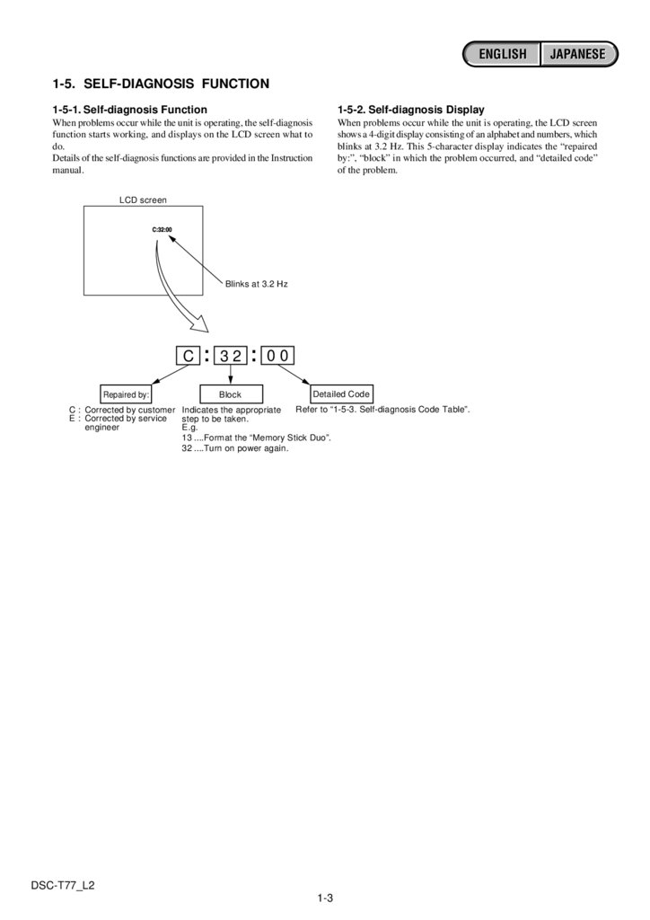
1-5. SELF-DIAGNOSIS FUNCTION
1-5-1. Self-diagnosis Function
1-5-2. Self-diagnosis Display
When problems occur while the unit is operating, the self-diagnosis
function starts working, and displays on the LCD screen what to
do.
Details of the self-diagnosis functions are provided in the Instruction
manual.
When problems occur while the unit is operating, the LCD screen
shows a 4-digit display consisting of an alphabet and numbers, which
blinks at 3.2 Hz. This 5-character display indicates the “repaired
by:”, “block” in which the problem occurred, and “detailed code”
of the problem.
LCD screen
Blinks at 3.2 Hz
C
Repaired by:
32
Block
00
Detailed Code
Refer to “1-5-3. Self-diagnosis Code Table”.
C : Corrected by customer Indicates the appropriate
E : Corrected by service
step to be taken.
engineer
E.g.
13 ....Format the “Memory Stick Duo”.
32 ....Turn on power again.
DSC-T77_L2
1-3
7.
ENGLISHJAPANESE
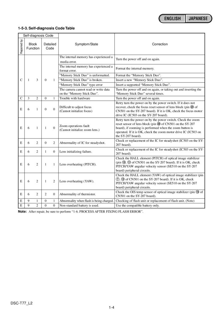
1-5-3. Self-diagnosis Code Table
Repaired by:
Self-diagnosis Code
Block
Function
Detailed
Code
C
1
3
0
1
C
3
2
0
1
E
6
1
0
0
E
6
1
1
0
E
6
2
0
2
E
6
2
1
0
E
6
2
1
1
E
6
2
1
2
E
6
2
2
0
E
E
9
9
1
2
0
0
1
0
Symptom/State
Correction
The internal memory has experienced a
media error.
The internal memory has experienced a
format error.
“Memory Stick Duo” is unformatted.
“Memory Stick Duo” is broken.
“Memory Stick Duo” type error
The camera cannot read or write data
on the “Memory Stick Duo”.
Trouble with hardware
Turn the power off and on again.
Format the internal memory.
Format the “Memory Stick Duo”.
Insert a new “Memory Stick Duo”.
Insert a supported “Memory Stick Duo”.
Turn the power off and on again, or taking out and inserting the
“Memory Stick Duo” several times.
Turn the power off and on again.
Retry turn the power on by the power switch. If it does not
Difficult to adjust focus
recover, check the focus reset sensor of lens block (pin w; of
(Cannot initialize focus)
CN501 on the SY-207 board). If it is OK, check the focus motor
drive IC (IC503 on the SY-207 board).
Retry turn the power on by the power switch. Check the zoom
reset sensor of lens block (pin wk of CN501 on the SY-207
Zoom operations fault
board), if zooming is performed when the zoom button is
(Cannot initialize zoom lens.)
operated. If it is OK, check the zoom motor drive IC (IC503 on
the SY-207 board).
Check or replacement of the IC for steadyshot (IC503 on the SYAbnormality of IC for steadyshot.
207 board).
Check or replacement of the IC for steadyshot (IC503 on the SYLens initializing failure.
207 board).
Check the HALL element (PITCH) of optical image stabilizer
(pin q;, qa of CN501 on the SY-207 board). If it is OK, check
Lens overheating (PITCH).
PITCH/YAW angular velocity sensor (SE510 on the SY-207
board) peripheral circuits.
Check the HALL element (YAW) of optical image stabilizer (pin
7, qs of CN501 on the SY-207 board). If it is OK, check
Lens overheating (YAW).
PITCH/YAW angular velocity sensor (SE510 on the SY-207
board) peripheral circuits.
Check the OIS temp sensor of optical image stabilizer (pin qk of
Abnormality of thermistor.
CN501 on the SY-207 board).
Abnormality when flash is being charged. Checking of flash unit or replacement of flash unit. (Note)
Non-standard battery is used.
Use the compatible battery only.
Note: After repair, be sure to perform “1-6. PROCESS AFTER FIXING FLASH ERROR”.
DSC-T77_L2
1-4
8.
ENGLISHJAPANESE
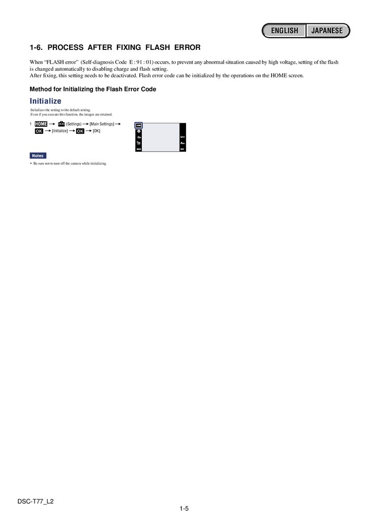
1-6. PROCESS AFTER FIXING FLASH ERROR
When “FLASH error” (Self-diagnosis Code E : 91 : 01) occurs, to prevent any abnormal situation caused by high voltage, setting of the flash
is changed automatically to disabling charge and flash setting.
After fixing, this setting needs to be deactivated. Flash error code can be initialized by the operations on the HOME screen.
Method for Initializing the Flash Error Code
Initialize
Initializes the setting to the default setting.
Even if you execute this function, the images are retained.
1
(Settings)
[Initialize]
[Main Settings]
[OK]
Notes
Be sure not to turn off the camera while initializing.
DSC-T77_L2
1-5
9.
1. SERVICE NOTEENGLISH
JAPANESE
1-1. SY-207基板交換時の注意
仕向けデータ
補修用基板と交換する時 補修用基板に書かれている仕向けデータは元の設定と違っている場合があります。
ADJ編を参照して 「DESTINATION DATA WRITE」を行ってください。
USBシリアルNo.
セットは 1台毎に異なる固有のID USB Serial No. を書き込んだ後 出荷されています。
新品の補修用基板には このIDが書き込まれていないので 基板交換後にIDを入力する必要があります。
ADJ編を参照して 「USB SERIAL No. INPUT」を行ってください。
角速度センサ
補修用基板と交換する時 角速度センサ SE510 の感度表示を書き留めてください。
ADJ編を参照して 「角速度センサ感度調整」を行ってください。
SY-207 BOARD (SIDE B)
YYY: YAW Sensor sensitivity
PPP: PITCH Sensor sensitivity
PPP
YYY
SE510
Note SY-207基板のSE510感度表示は補修用基板にしか記載されておりません。
1-2. レンズ交換時の注意
レンズ交換時、補修用レンズ添付データシート掲載のPITCH/YAWデータ、FNデータおよびW端調整データを書き留めてください。
ADJ編を参照して 「W端調整」 「角速度センサ感度調整」を行ってください。
Wide Limit Data (2-byte data)
XXYY
XX
YY
FN Data
FN
XX
FN data
L 1 /L 2
PITCH/YAW Data
P.PP / Y.YY
YAW data
PITCH data
Note PITCH/YAWデータ、FNデータおよびW端調整データは、
補修用部品にのみ記載されています。
DSC-T77_L2
1-6
10.
ENGLISHJAPANESE
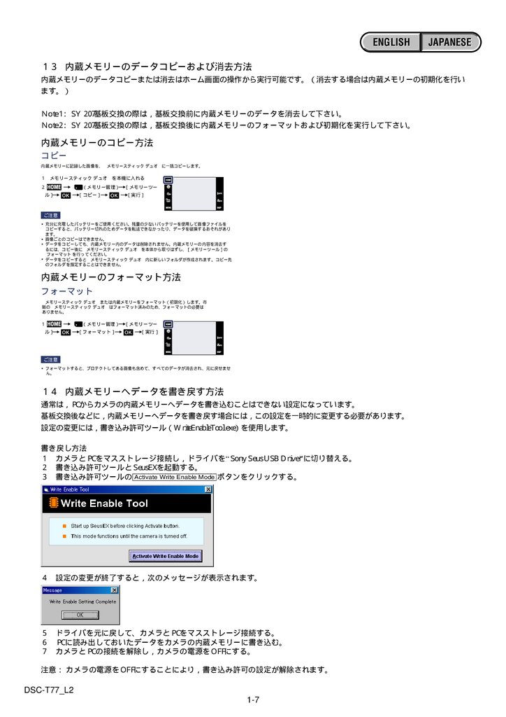
1-3. 内蔵メモリーのデータコピーおよび消去方法
内蔵メモリーのデータコピーまたは消去はホーム画面の操作から実行可能です。 消去する場合は内蔵メモリーの初期化を行い
ます。
Note1 SY-207基板交換の際は 基板交換前に内蔵メモリーのデータを消去して下さい。
Note2 SY-207基板交換の際は 基板交換後に内蔵メモリーのフォーマットおよび初期化を実行して下さい。
内蔵メモリーのコピー方法
コピー
内蔵メモリーに記録した画像を、 メモリースティック デュオ に一括コピーします。
1
メモリースティック デュオ
2
を本機に入れる
メモリー管理
ル
コピー
メモリーツー
実行
ご注意
充分に充電したバッテリーをご使用ください。残量の少ないバッテリーを使用して画像ファイルを
コピーすると、バッテリー切れのためデータを転送できなかったり、データを破損するおそれがあり
ます。
画像ごとのコピーはできません。
データをコピーしても、内蔵メモリー内のデータは削除されません。内蔵メモリーの内容を消去す
るには、コピー後に メモリースティック デュオ を本体から取りはずし、 メモリーツール の
[フォーマット]を行ってください。
データをコピーすると メモリースティック デュオ 内に新しいフォルダが作成されます。コピー先
のフォルダを指定することはできません。
内蔵メモリーのフォーマット方法
フォーマット
メモリースティック デュオ または内蔵メモリーをフォーマット 初期化 します。市
販の メモリースティック デュオ はフォーマット済みのため、フォーマットの必要は
ありません。
1
メモリー管理 メモリーツー
ル
フォーマット
実行
ご注意
フォーマットすると、プロテクトしてある画像も含めて、すべてのデータが消去され、元に戻せませ
ん。
1-4. 内蔵メモリーへデータを書き戻す方法
通常は PCからカメラの内蔵メモリーへデータを書き込むことはできない設定になっています。
基板交換後などに 内蔵メモリーへデータを書き戻す場合には この設定を一時的に変更する必要があります。
設定の変更には 書き込み許可ツール WriteEnableTool.exe を使用します。
書き戻し方法
1) カメラとPCをマスストレージ接続し ドライバを“Sony Seus USB Driver”に切り替える。
2) 書き込み許可ツールとSeusEXを起動する。
3) 書き込み許可ツールの[Activate Write Enable Mode]ボタンをクリックする。
4)
設定の変更が終了すると 次のメッセージが表示されます。
5)
6)
7)
ドライバを元に戻して、カメラとPCをマスストレージ接続する。
PCに読み出しておいたデータをカメラの内蔵メモリーに書き込む。
カメラとPCの接続を解除し カメラの電源をOFFにする。
注意 カメラの電源をOFFにすることにより 書き込み許可の設定が解除されます。
DSC-T77_L2
1-7
11.
ENGLISHJAPANESE
1-5. 自己診断機能
1-5-2. 自己診断表示
本機の動作に不具合が生じたとき LCD画面にアルファベッ
トと4桁の数字が表示され 3.2Hzで点滅します。この5文字
の表示によって対応者分類および不具合の生じたブロックの
分類 不具合の詳細コードを示します。
1-5-1. 自己診断機能について
本機の動作に不具合が生じたとき 自己診断機能が働き
L C D 画面に どう処置したらよいか判断できる表示を行い
ます。自己診断機能については取扱説明書にも掲載されて
います。
LCD画面
C : 3 2 : 00
3.2Hz点滅
C
対応者分類
C お客さま自身で対応
E サービスエンジニア
で対応
32
ブロック分類
00
詳細コード
「1-5 -3 . 自己診断コード表」
対応方法の違いにより分類
例 13 “メモリースティック を参照
デュオ”をフォーマッ
トする
32 電源を入れ直す
DSC-T77_L2
1-8
12.
ENGLISHJAPANESE
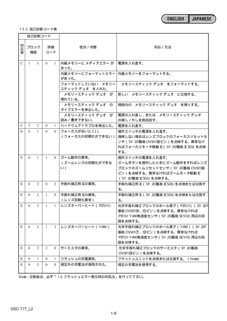
1-5-3. 自己診断コード表
自己診断コード
対 ブロック
応
機能
者
詳細
コード
C
0
1
3
1
症状 状態
対応 方法
内蔵メモリーに メディアエラー が
あった。
電源を入れ直す。
内蔵メモリーにフォーマットエラー 内蔵メモリーをフォーマットする。
があった。
フォーマットしていない メモリー
スティック デュオ を入れた。
メモリースティック デュオ
をフォーマットする。
メモリースティック デュオ
壊れている。
が
新しい
メモリースティック デュオ
メモリースティック デュオ
タイプエラーを検出した。
の
規格内の
メモリースティック デュオ
読み 書きできない。
が
電源の入れ直し または メモリースティック デュオ
の挿し 外しを数回試す。
メモリースティック デュオ
に交換する。
を挿入する。
C
3
2
0
1
ハードウェアトラブルを検出した。 電源を入れ直す。
E
6
1
0
0
フォーカスが合いにくい。
操作スイッチの電源を入れ直す。
フォーカスの初期化ができない 復帰しない場合はレンズブロックのフォーカスリセットセ
ンサ SY-207基板CN501 w;ピン を点検する。異常なけ
ればフォーカスモータ駆動IC SY-207基板IC503 を点検
する。
E
6
1
1
0
ズーム動作の異常。
ズームレンズの初期化ができな
い
操作スイッチの電源を入れ直す。
ズームボタンを操作したときにズーム動作をすればレンズ
ブロックのズームリセットセンサ SY-207基板CN501 wk
ピン を点検する。異常なければズームモータ駆動IC
SY-207基板IC503 を点検する。
E
6
2
0
2
手振れ補正用ICの異常。
手振れ補正用IC SY-207基板IC503 を点検または交換す
る。
E
6
2
1
0
手振れ補正用ICの異常。
レンズ初期化異常
手振れ補正用IC SY-207基板IC503 を点検または交換す
る。
E
6
2
1
1
レンズオーバーヒート PITCH
光学手振れ補正ブロックのホール素子 PITCH SY-207
基板CN501 q; qaピン を点検する。異常なければ
PITCH/YAW角速度センサ SY-207基板SE510 周辺の回
路を点検する。
E
6
2
1
2
レンズオーバーヒート YAW
光学手振れ補正ブロックのホール素子 YAW SY-207
基板CN501 7 qsピン を点検する。異常なければ
PITCH/YAW角速度センサ SY-207基板SE510 周辺の回
路を点検する。
E
6
2
2
0
サーミスタの異常。
光学手振れ補正ブロックのサーミスタ SY-207基板
CN501 qkピン を点検する。
E
9
1
0
1
フラッシュの充電異常。
フラッシュユニットを点検または交換する。 Note
E
9
2
0
0
規定外の充電池が使用された。
規定の充電池を使用する。
Note 交換後は 必ず「1-6. フラッシュエラー発生時の対処法」を行って下さい。
DSC-T77_L2
1-9
13.
ENGLISHJAPANESE
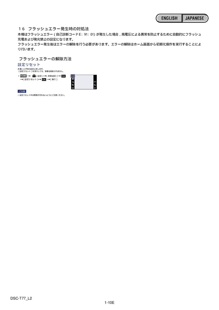
1-6. フラッシュエラー発生時の対処法
本機はフラッシュエラー 自己診断コードE 91 01 が発生した場合 高電圧による異常を防止するために自動的にフラッシュ
充電および発光禁止の設定になります。
フラッシュエラー発生後はエラーの解除を行う必要があります。エラーの解除はホーム画面から初期化操作を実行することによ
り行います。
フラッシュエラーの解除方法
設定リセット
お買い上げ時の設定に戻します。
設定リセット を実行しても、画像は削除されません。
1
設定
設定リセット
本体設定
実行
ご注意
設定リセット中は電源が切れないようにご注意ください。
DSC-T77_L2
1-10E
14.
2. DISASSEMBLYNOTE FOR REPAIR
• Make sure that the flat cable and flexible board are not cracked of bent at the terminal.
Do not insert the cable insufficiently nor crookedly.
Cut and remove the part of gilt
which comes off at the point.
(Be careful or some
pieces of gilt may be left inside)
• When remove a connector, don’t pull at wire of connector. It is possible that a wire is snapped.
• When installing a connector, don’t press down at wire of connector.
It is possible that a wire is snapped.
• Do not apply excessive load to the gilded flexible board.
DISCHARGING OF THE ST-199 FLEXIBLE BOARD’S CHARGING CAPACITOR
(C901, C902)
The charging capacitor (C901, C902) of the ST-199 flexible board
is charged up to the maximum 315 V potential.
There is a danger of electric shock by this high voltage when the
capacitor is handled by hand. The electric shock is caused by
the charged voltage which is kept without discharging when the
main power of the unit is simply turned off. Therefore, the
remaining voltage must be discharged as described below.
C901
C902
Capacitors
Preparing the Short Jig
To preparing the short jig, a small clip is attached to each end of
a resistor of 1 kΩ /1 W (1-215-869-11).
Wrap insulating tape fully around the leads of the resistor to
prevent electrical shock.
SY
-20
7
1 kΩ/1 W
Wrap insulating tape.
Note: High-voltage cautions
Discharging the Capacitor
Short-circuit between the two points
with the short jig about 10 seconds.
To avoid the spark with the metal plate,
wrap the short jig with the insulation tape.
R:1 kΩ/1 W
(Part code: 1-215-869-11)
ST-199 Flexible
Board
DSC-T77_L2
2-1
15.
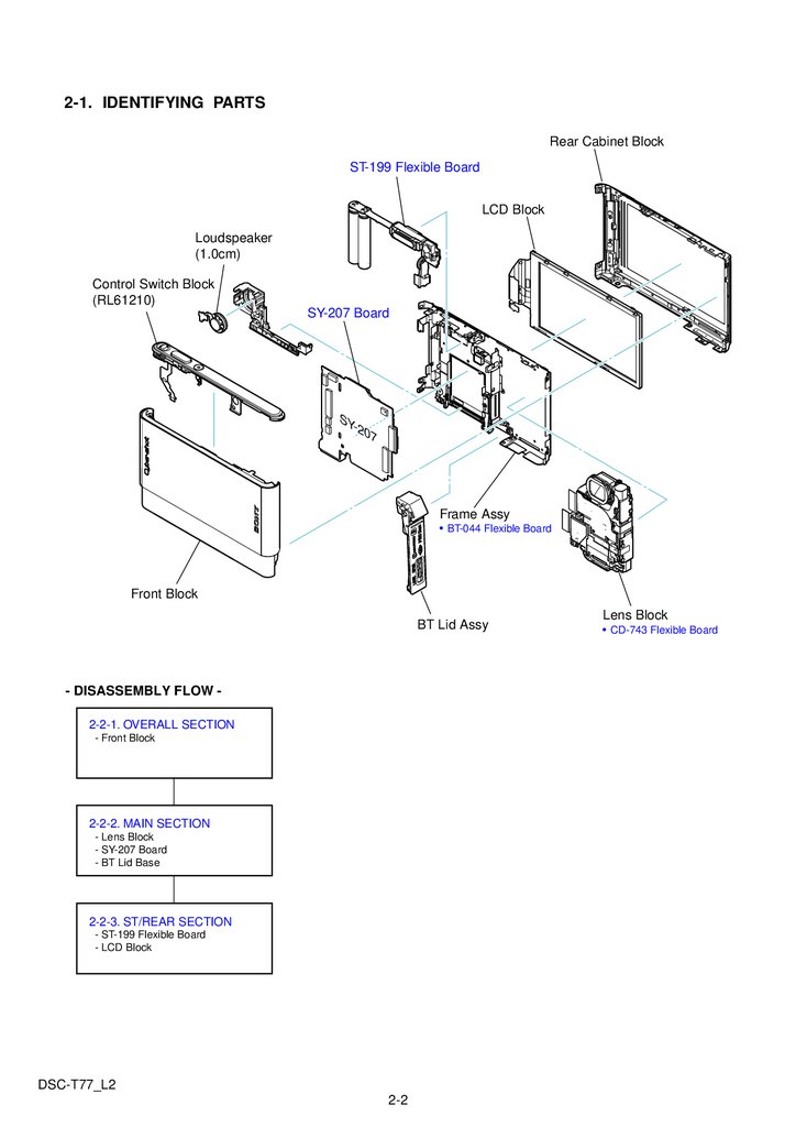
2-1. IDENTIFYING PARTSRear Cabinet Block
ST-199 Flexible Board
LCD Block
Loudspeaker
(1.0cm)
Control Switch Block
(RL61210)
SY-207 Board
SY
-20
7
Frame Assy
BT-044 Flexible Board
Front Block
BT Lid Assy
- DISASSEMBLY FLOW 2-2-1. OVERALL SECTION
- Front Block
2-2-2. MAIN SECTION
- Lens Block
- SY-207 Board
- BT Lid Base
2-2-3. ST/REAR SECTION
- ST-199 Flexible Board
- LCD Block
DSC-T77_L2
2-2
Lens Block
CD-743 Flexible Board
16.
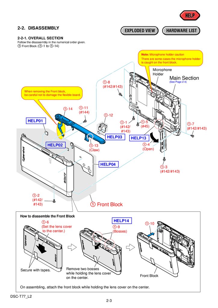
HELP2-2. DISASSEMBLY
EXPLODED VIEW
HARDWARE LIST
2-2-1. OVERALL SECTION
Follow the disassembly in the numerical order given.
1 Front Block (1-1 to 1-14)
Note: Microphone holder caution
There are some cases the microphone holder
is caught on the front block.
Microphone
Holder
Main Section
(See Page 2-4)
1-8
(#142/#143)
When removing the Front block,
be careful not to damage the flexible board.
1-14
1-11
(#144)
1-12
HELP01
1-1
(#142/
#143)
HELP03
HELP02
1-5
(#45)
HELP13
1-4
(Open)
1-13
(Claw)
HELP04
1-2
(#142/
#143)
1-3
(#142/#143)
1 Front Block
How to diassemble the Front Block
HELP14
1-6
(Set the lens cover
to the center.)
Secure with tapes.
1-7
(#142/#143)
1-10
1-9
(Bosses)
Remove two bosses
while holding the lens cover
on the center.
Front Block
On assembling, attach the front block while holding the lens cover on the center.
DSC-T77_L2
2-3
17.
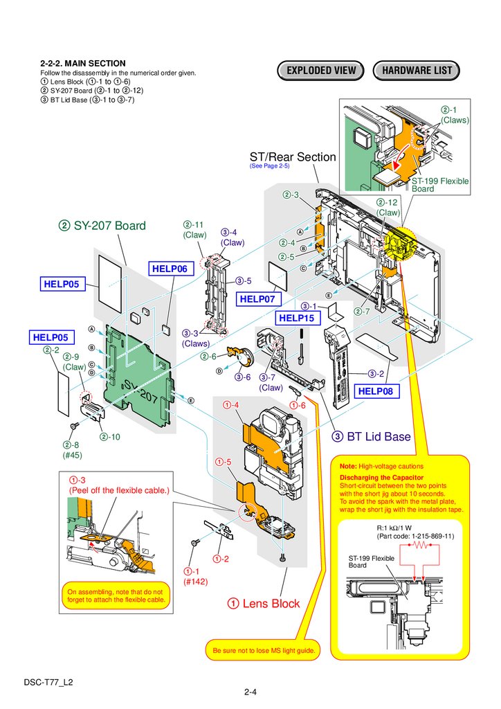
2-2-2. MAIN SECTIONEXPLODED VIEW
Follow the disassembly in the numerical order given.
1 Lens Block (1-1 to 1-6)
2 SY-207 Board (2-1 to 2-12)
3 BT Lid Base (3-1 to 3-7)
HARDWARE LIST
2-1
(Claws)
ST/Rear Section
(See Page 2-5)
ST-199 Flexible
Board
2-3
2-12
(Claw)
(Claw)
2 SY-207 Board
2-11
(Claw)
3-4
(Claw)
A
2-4
B
2-5
HELP06
C
3-5
HELP05
E
HELP07
3-1
HELP15
A
3-3
(Claws)
HELP05
B
2-2
2-7
2-6
2-9
(Claw) C
D
D
3-2
3-6 3-7
(Claw)
SY
-20
7
E
1-4
HELP08
1-6
3 BT Lid Base
2-10
2-8
(#45)
1-5
Note: High-voltage cautions
Discharging the Capacitor
Short-circuit between the two points
with the short jig about 10 seconds.
To avoid the spark with the metal plate,
wrap the short jig with the insulation tape.
1-3
(Peel off the flexible cable.)
R:1 kΩ/1 W
(Part code: 1-215-869-11)
ST-199 Flexible
Board
1-2
1-1
(#142)
On assembling, note that do not
forget to attach the flexible cable.
1 Lens Block
Be sure not to lose MS light guide.
DSC-T77_L2
2-4
18.
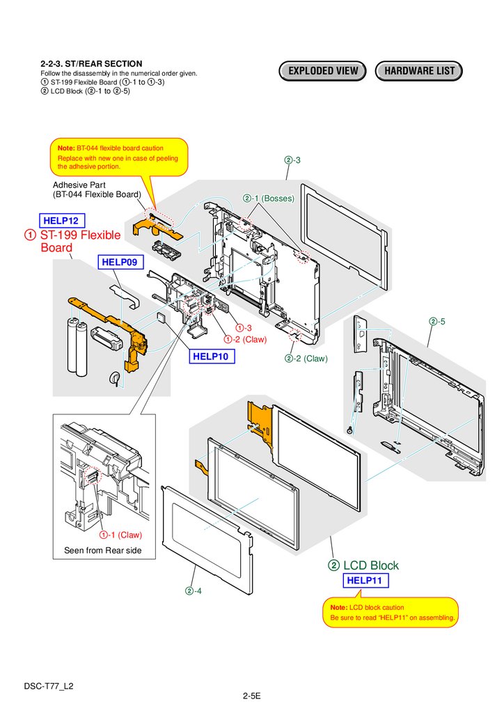
2-2-3. ST/REAR SECTIONEXPLODED VIEW
Follow the disassembly in the numerical order given.
1 ST-199 Flexible Board (1-1 to 1-3)
2 LCD Block (2-1 to 2-5)
Note: BT-044 flexible board caution
Replace with new one in case of peeling
the adhesive portion.
HARDWARE LIST
2-3
Adhesive Part
(BT-044 Flexible Board)
2-1 (Bosses)
HELP12
1 ST-199 Flexible
Board
HELP09
2-5
1-3
1-2 (Claw)
HELP10
2-2 (Claw)
1-1 (Claw)
Seen from Rear side
2 LCD Block
HELP11
2-4
Note: LCD block caution
Be sure to read “HELP11” on assembling.
DSC-T77_L2
2-5E
19.
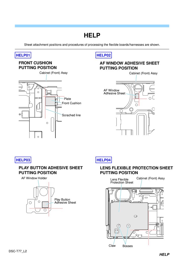
HELPSheet attachment positions and procedures of processing the flexible boards/harnesses are shown.
HELP01
HELP02
FRONT CUSHION
PUTTING POSITION
AF WINDOW ADHESIVE SHEET
PUTTING POSITION
Cabinet (Front) Assy
Cabinet (Front) Assy
AF Window
Adhesive Sheet
Plate
Front Cushion
Scrached line
HELP03
HELP04
PLAY BUTTON ADHESIVE SHEET
PUTTING POSITION
AF Window Holder
LENS FLEXIBLE PROTECTION SHEET
PUTTING POSITION
Lens Flexible
Protection Sheet
Cabinet (Front) Assy
Play Button
Adhesive Sheet
Claw
Bosses
DSC-T77_L2
HELP
20.
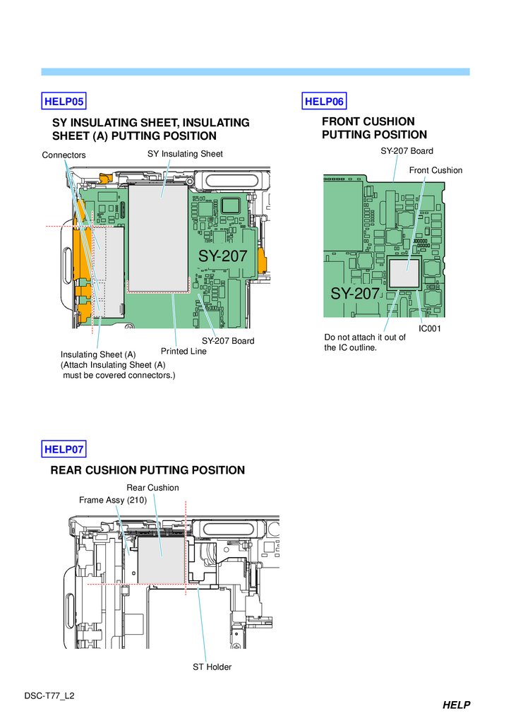
HELP05HELP06
SY INSULATING SHEET, INSULATING
SHEET (A) PUTTING POSITION
Connectors
FRONT CUSHION
PUTTING POSITION
SY-207 Board
SY Insulating Sheet
Front Cushion
SY-207
SY-207
IC001
IC
SY-207 Board
Printed Line
Insulating Sheet (A)
(Attach Insulating Sheet (A)
must be covered connectors.)
Do not attach it out of
the IC outline.
HELP07
REAR CUSHION PUTTING POSITION
Rear Cushion
Frame Assy (210)
ST Holder
DSC-T77_L2
HELP
21.
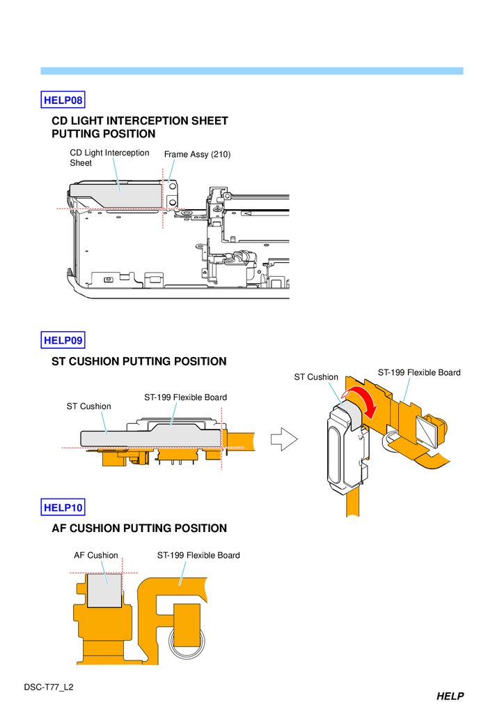
HELP08CD LIGHT INTERCEPTION SHEET
PUTTING POSITION
CD Light Interception
Sheet
Frame Assy (210)
HELP09
ST CUSHION PUTTING POSITION
ST Cushion
ST-199 Flexible Board
ST-199 Flexible Board
ST Cushion
HELP10
AF CUSHION PUTTING POSITION
AF Cushion
ST-199 Flexible Board
DSC-T77_L2
HELP
22.
HELP11INSTALLATION CAUTIONS OF THE LCD BLOCK
1 Attach four claws of FTS block assy (30SHGU08) to the light guide plate (3.0) block in the order A, B, C and D.
FTS Block Assy
(30SHGU08)
Claw A
Adjust to the upper
left standard.
FTS Block Assy
(30SHGU08)
Claw B
Claw C
Claw D
Light Guide
Plate (3.0) Block
Light Guide
Plate (3.0) Block
2 Attach two claws of FTS block assy (30SHGU08)
to the light guide plate (3.0) block in the order E and F.
And check the claws fit properly.
Confirm the claw is caught
precisely.
Claws
FTS Block Assy
(30SHGU08)
Check the bezel fits under the convex portion
properly. (In case of attaching FTS block assy
(30SHGU08) in the condition the convex
portion is over the bezel, the LCD panel is
broken.)
Convex portion of
Light Guide Plate (3.0) Block
Claw F
Bezel of
FTS Block Assy
(30SHGU08)
Claw E
Confirm the claw is caught
precisely.
Light Guide
Plate (3.0) Block
DSC-T77_L2
HELP
23.
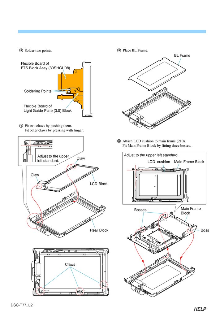
5 Place BL Frame.3 Solder two points.
BL Frame
Flexible Board of
FTS Block Assy (30SHGU08)
Soldering Points
Flexible Board of
Light Guide Plate (3.0) Block
4 Fit two claws by pushing them.
Fit other claws by pressing with finger.
6 Attach LCD cushion to main frame (210).
Fit Main Frame Block by fitting three bosses.
Adjust to the upper
left standard.
Adjust to the upper left standard.
Claw
LCD cushion
Main Frame Block
Claw
LCD Block
Bosses
Rear Block
Main Frame
Block
Boss
Claws
DSC-T77_L2
HELP
24.
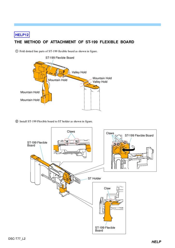
HELP12THE METHOD OF ATTACHMENT OF ST-199 FLEXIBLE BOARD
1 Fold dotted line parts of ST-199 flexible board as shown in figure.
ST-199 Flexible Board
Valley Hold
Mountain Hold
Mountain Hold
Valley Hold
Mountain Hold
Mountain Hold
2 Install ST-199 Flexible board to ST holder as shown in figure.
Claws
Claws
ST-199 Flexible Board
ST-199 Flexible
Board
ST Holder
Claw
ST-199 Flexible
Board
DSC-T77_L2
HELP
25.
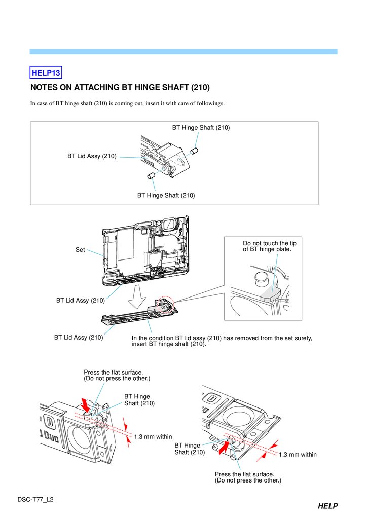
HELP13NOTES ON ATTACHING BT HINGE SHAFT (210)
In case of BT hinge shaft (210) is coming out, insert it with care of followings.
BT Hinge Shaft (210)
BT Lid Assy (210)
BT Hinge Shaft (210)
Do not touch the tip
of BT hinge plate.
Set
BT Lid Assy (210)
BT Lid Assy (210)
In the condition BT lid assy (210) has removed from the set surely,
insert BT hinge shaft (210).
Press the flat surface.
(Do not press the other.)
BT Hinge
Shaft (210)
1.3 mm within
BT Hinge
Shaft (210)
1.3 mm within
Press the flat surface.
(Do not press the other.)
DSC-T77_L2
HELP
26.
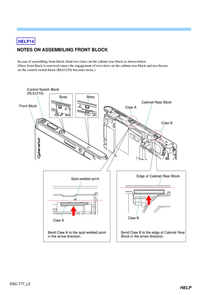
HELP14NOTES ON ASSEMBILING FRONT BLOCK
In case of assembling front block, bend two claws on the cabinet rear block as shown below.
(Once front block is removed causes the engagement of two claws on the cabinet rear block and two bosses
on the control switch block (RL61210) becomes loose.)
Control Switch Block
(RL61210)
Boss
Boss
Cabinet Rear Block
Front Block
Claw A
Claw B
Spot-welded point
Claw A
Bend Claw A to the spot-welded point
in the arrow direction.
Edge of Cabinet Rear Block
Claw B
Bend Claw B to the edge of Cabinet Rear
Block in the arrow direction.
DSC-T77_L2
HELP
27.
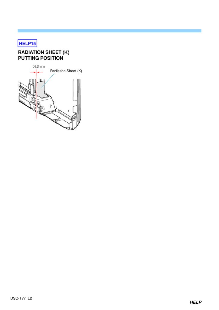
HELP15RADIATION SHEET (K)
PUTTING POSITION
0 3mm
Radiation Sheet (K)
DSC-T77_L2
HELP
28.
3. BLOCK DIAGRAMSLink
OVERALL BLOCK DIAGRAM (1/2)
POWER BLOCK DIAGRAM (1/2)
OVERALL BLOCK DIAGRAM (2/2)
POWER BLOCK DIAGRAM (2/2)
DSC-T77_L2
29.
3. BLOCK DIAGRAMS3-1. OVERALL BLOCK DIAGRAM (1/2)
SUB_CONT
Q302
CPU,
CAMERA DSP,
AV SIGNAL PROCESS,
LENS CONTROL,
MODE CONTROL
VSUB_CONT_PRE,
VSUB_CONT_POST
Q301
V8
LENS TEMP
SENSOR
LENS_TEMP
18
W16, AD25, Y18, Y17
AE8
IC_211_2_SO,
XIC_211_2_SCK
XCS_AUDIO
ZM_DIR_A, ZM_DIR_B, ZM_BRK_A
FC_SENS
XFC_RST_LED
ZM_SENS_1ST
XZM_RST_LED
FC_SENS
Y10
XFC_RST_LED
M8
ZM_SENS_1ST
AD26
XZM_RST_LED
J8
LENS_TEMP
LENS_TEMP
AE3
2
BL_H
OVERALL (2/2)
(PAGE 3-2)
BL_L
45
44
MIC601
(MICROPHONE)
D6
IC_211_AUIN
A6
IC_211_AUOUT
B6
A3
IC601
AUDIO/VIDEO
AMP
(8/9)
CN711
SP±
SP901
(LOUDSPEAKER)
CN705
(1/2)
W18, AB26, W17
FC_DIR_A, FC_DIR_B, FC_BRK_A
AB23, AC26, AA23
K2, J3 - J5
G4, H3, J1, J2
B1, C3, D4, D5
K9, J6 - J8
32 - 35
20
19
28
30
IRIS_DIR_A, IRIS_BRK_A,
IRIS_DIR_B, IRIS_BRK_B
IC_211_
YOUT
F3
E2
E1
F1
IC_211_YOUT
AB13
IC_211_PBOUT
AF12
IC_211_PROUT
AC12
Y1, AA1
FC_SENS
XFC_RST_LED
ZM_SENS_1ST
XZM_RST_LED
ZOOM_A, ZOOM_B,
ZOOM_A, ZOOM_B
OPTICAL IMAGE
STABILIZATION DRIVE,
LENS DRIVE,
IRIS MOTOR DRIVER,
FOCUS MOTOR DRIVER,
ZOOM MOTOR DRIVER
(7/9)
A2, B3 - B5
ZOOM_A, XA, B, XB
FOCUS_A, FOCUS_B,
FOCUS_A, FOCUS_B
23 - 26
FOCUS_A, XA, B, XB
36 - 39
IRIS_A, XA, B, XB
IC503
(1/2)
IRIS_A, IRIS_B,
IRIS_A, IRIS_B
G7, H8, J9, J10
AF8
CN501
10 - 17
LCD
BACKLIGHT
XDD_SYS_RST
XCS_FE, XIC_211_3_SCK, IC_211_3_SO
7-9
IC_211_2_SO, XIC_211_2_SCK
Y13
Y12
(3/9, 4/9, 5/9)
F3
4
3
5, 6
AB19 - AB 21, AC18
- AC21, AE18 - AE21
,AF19 - AF21
U19
3.0 inch
COLOR
LCD
MONITOR
1,2, 5,6
LV1
SUB
XCS_ PANEL
XDD_SYS_RST
IC211
(1/2)
IC304
CCD SIGNAL
PROCESS,
TIMING
E3
K5 GENERATOR
(6/9)
H7
VHLD1, VHLD2
LCD_CK, LCD_HD, LCD_VD
AU_LINE_OUT
V_LINE_OUT
IC_211_YOUT_FB
IC_211_PBOUT_FB
IC_211_PROUT_FB
16
20
24
4
2
MULTI
CONNECTOR
(1/2)
12, 10
VST1, VST2
GEN_TG_CLK
GEAR_ON
GEN_SYS_CLK
IC202
1
CLOCK
3
GENERATOR
5
(2/9)
LCD_D0 - LCD_D7
A1, C1
V1, V2, V4, V6-V10,
V3A, V3B, V5A, V5B
2
D17, B19, E17, A19,
B18, D18, B17 E16, A18, D16, A17
B11, C11,
D11
J6 - J8, L8
-L11, K6 - K10
X201
38MHz
LCD901 (1/2)
CN709
E6, D5
24
13
16
F11
H11
AE23
AF22
AF18
E18, B23
LV
SUB
SUB_CONT
CA_HD
CA_FD
GEN_TG_CLK
A10
E8
B7
C25, D19, V19
VHLD1, VHLD2
CA_AD00 - CA_AD13
F1, D4, E1
VST1, VST2
4
1
29
LH1
RG
H5, L6 H6, L7
6 - 17
FOCUS
RESET
SENSOR
J5
H1 - H3
5
3
V1A, V1B, V2, V3A - V3C,
V4, V5A - V5C, V6S1, V6S2
37, 38 19, 18
ZOOM
RESET
SENSOR
LH1
RG
33
23
M
10 - 8
M
G1
LV2
23
H1 - H3
A2
POWER_SAVE
18
15, 17 35, 37 25 - 34, 36, 38
M
IRIS
MOTOR
34 - 36
FOCUS
MOTOR
P/S
VOG
3
CCDOUT
20
14
1, 16
HIGH SPEED
BUFFER
AMP
IC001
CCD
IMAGER
IC002
10
20
G3, G4, H2 - H4,
J2 - J4, K1, K3, K4
L3 - L5
CN301
IRIS
(METER)
ZOOM
MOTOR
SY-207 BOARD (1/2)
R7, AF25
CD-743 FLEXIBLE BOARD
LENS BLOCK
LENS
( ) : Number in parenthesis ( ) indicates the division number of schematic diagram where the component is located.
USB_DP, USB_DM
M
HALL
ELEMENT
PITCH±
PITCH_HALLBAIS±,
PITCH_HALL±
CLK, DATA
PITCH_AD
24, 25
OPTICAL IMAGE
STABILIZATION DRIVE,
LENS DRIVE,
IRIS MOTOR DRIVER, D1
FOCUS MOTOR DRIVER,
ZOOM MOTOR DRIVER
A10
(7/9)
E8
E9
E7
B2
G5, K1
IC503
(2/2)
PITCH/YAW
SENSOR 21
AMP
(7/9)
SE510
PITCH/YAW
SENSOR
MSX_BS, MSX_D0 - MSX_D3, MSX_CLK
XMS_IN
CN702
6
MEMORY
STICK
PRO DUO
10
CA_FD
XDD_SYS_RST
CLK_IC_503
XIC_211_IC_503_RST
XCS_IC_503
CLK_IC_503
W13
XIC_211_IC_503_RST
H10
XCS_IC_503
U8
XDD_SYS_RST
A1, C4, C5
OVERALL (2/2)
(PAGE 3-2)
2 - 5, 7, 8
3
13
A13 - A15,
B13 - B15
B6, B7
YAW_AD
IC506
C9, F1 - F3
PITCH
MOTOR
YAW_HALLBAIS±,
YAW_HALL±
C2
F8, F10, G8, G9 B8, A9
HALL
ELEMENT
YAW±
7 - 9, 12
M
10, 11, 13, 14 1, 16
YAW
MOTOR
2-5
OPTICAL IMAGE
STABILIZER
IC_211_0_SO, IC_211_0_SI, XIC_211_0_SCK
1
OVERALL (2/2)
(PAGE 3-2)
DSC-T77_L2
3-1
A : VIDEO SIGNAL
A : AUDIO SIGNAL
A : VIDEO/AUDIO SIGNAL
30.
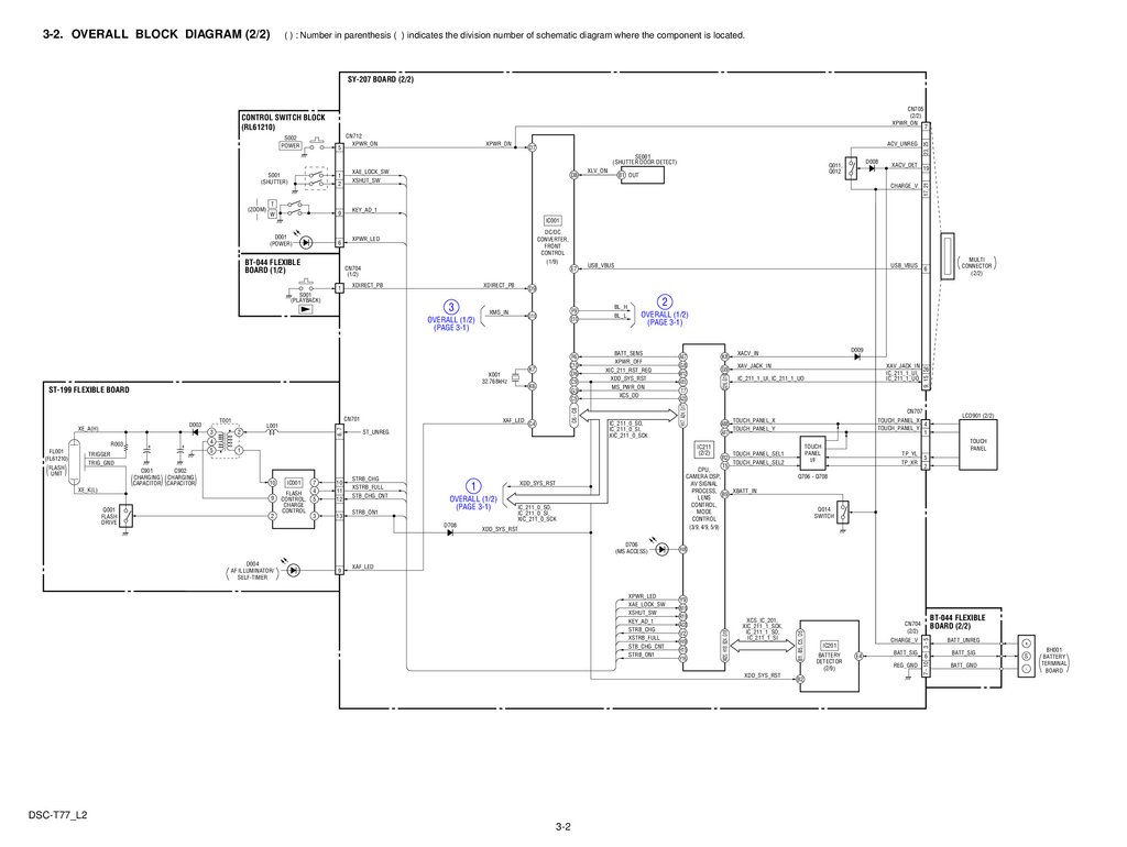
3-2. OVERALL BLOCK DIAGRAM (2/2)( ) : Number in parenthesis ( ) indicates the division number of schematic diagram where the component is located.
SY-207 BOARD (2/2)
5
CN712
XPWR_ON
XPWR_ON
ACV_UNREG
D7
SE001
(SHUTTER DOOR DETECT)
S001
(SHUTTER)
(ZOOM)
1
2
XAE_LOCK_SW
XSHUT_SW
D8
XLV_ON
D008
Q011,
Q012
B1 OUT
XACV_DET
CHARGE_V
7
19
17, 21
S002
POWER
23, 25
CN705
(2/2)
XPWR_ON
CONTROL SWITCH BLOCK
(RL61210)
T
9
W
KEY_AD_1
IC001
CN704
(1/2)
XDIRECT_PB
3
XMS_IN
K6
(FLASH
UNIT )
+
5
C901
C902
CHARGING CHARGING
CAPACITOR CAPACITOR
(
)(
ST_UNREG
BATT_SENS
XPWR_OFF
XIC_211_RST_REQ
XDD_SYS_RST
MS_PWR_ON
XCS_DD
IC_211_0_SO,
IC_211_0_SI,
XIC_211_0_SCK
)
K8
AE7
G8
W12
AB18
T7
A23
G9
10
9
2
IC001
FLASH
CONTROL,
CHARGE
CONTROL
7
4
5
3
10
11
12
13
STRB_CHG
XSTRB_FULL
STB_CHG_CNT
STRB_ON1
OVERALL (1/2)
(PAGE 3-1)
D708
IC_211_0_SO,
IC_211_0_SI,
XIC_211_0_SCK
XDD_SYS_RST
D706
(MS ACCESS)
D004
AF ILLUMINATOR/
SELF-TIMER
9
XAV_JACK_IN
XAV_JACK_IN
26
IC_211_1_UI,
IC_211_1_UO
IC_211_1_UI, IC_211_1_UO
CN707
TOUCH_PANEL_X
4
TOUCH_PANEL_Y
1
LCD901 (2/2)
TOUCH
PANEL
TOUCH
PANEL
I/F
TOUCH_PANEL_SEL1
R2
TOUCH_PANEL_SEL2
T5
CPU,
CAMERA DSP,
AV SIGNAL
PROCESS,
XBATT_IN
B9
LENS
CONTROL,
MODE
CONTROL
(3/9, 4/9, 5/9)
XDD_SYS_RST
1
D009
XACV_IN
TOUCH_PANEL_X
AB8
TOUCH_PANEL_Y
AF7
IC211
(2/2)
1
XE_K(L)
Q001
FLASH
DRIVE
C4
2
TP_YL
TP_XR
5
2
Q706 - Q708
Q014
SWITCH
H8
XAF_LED
XPWR_LED
XAE_LOCK_SW
XSHUT_SW
KEY_AD_1
STRB_CHG
XSTRB_FULL
STB_CHG_CNT
STRB_ON1
Y9
N19
R19
AC8
V2
H9
H15
Y16
XCS_IC_201,
XIC_211_1_SCK,
IC_211_1_SO,
IC_211_1_SI
XDD_SYS_RST
DSC-T77_L2
3-2
B2
BT-044 FLEXIBLE
BOARD (2/2)
CN704
(2/2)
CHARGE_V
IC201
BATTERY
DETECTOR
(2/9)
E4
BATT_SIG
REG_GND
3-5
+
MULTI
CONNECTOR
(2/2)
OVERALL (1/2)
(PAGE 3-1)
4
TRIGGER
TRIG_GND
6
6
7 - 10
FL001
(FL61210)
2
XAF_LED
BL_H
BL_L
B1, B5, C5, D5
3
R003
6, 7
XE_A(H)
L001
F6
C10
D6
C9
G3
C5
K7
ST-199 FLEXIBLE BOARD
D003
F9
E10
D10
X001
32.768kHz
CN701
USB_VBUS
D9
OVERALL (1/2)
(PAGE 3-1)
T001
USB_VBUS
9, 15
XDIRECT_PB
S001
(PLAYBACK)
C6 - C8
1
E7
D26, G19
BT-044 FLEXIBLE
BOARD (1/2)
XPWR_LED
W20, H18, B24, G18
6
H17, A24, G17
D001
(POWER)
DC/DC
CONVERTER,
FRONT
CONTROL
(1/9)
BATT_UNREG
BATT_SIG
BATT_GND
+
S
-
BH001
BATTERY
TERMINAL
BOARD
31.
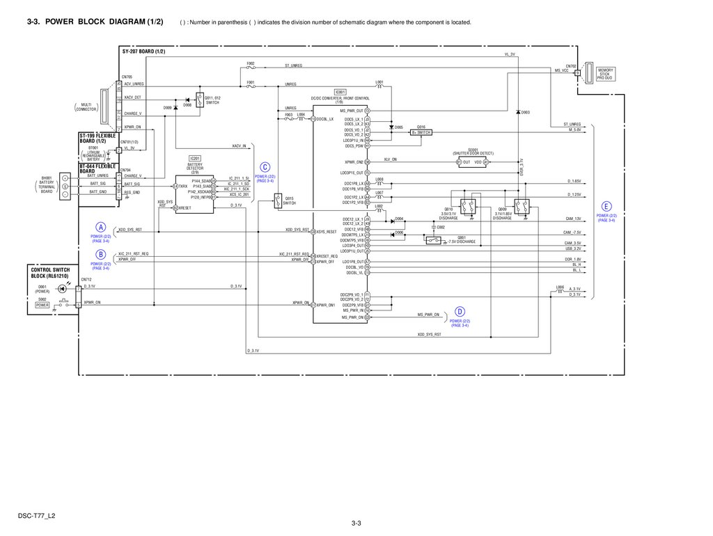
3-3. POWER BLOCK DIAGRAM (1/2)( ) : Number in parenthesis ( ) indicates the division number of schematic diagram where the component is located.
SY-207 BOARD (1/2)
VL_3V
F002
ST_UNREG
CN702
MS_VCC
9
23, 25
CN705
F001
ACV_UNREG
MEMORY
STICK
PRO DUO
L001
UNREG
IC001
MULTI
CONNECTOR
17, 21
D009
ST-199 FLEXIBLE
BOARD (1/2)
BT001
LITHIUM
RECHARGEABLE
BATTERY
BATT_SIG
S
BATT_GND
-
MS_PWR_OUT F3
2
F10 DDCBL_LX
D001
(POWER)
SE001
(SHUTTER DOOR DETECT)
IC201
3-5
CHARGE_V
P144_SDA0 D5
P143_SIA0 C5
E4 TXRX
P142_XSCKA0 B5
P120_INTP0 B1
BATT_SIG
REG_GND
B2 XRESET
XLV_ON
XPWR_ON2 D8
BATTERY
DETECTOR
(2/9)
CN704
6
ST_UNREG
M_5.0V
Q016
B+ SWITCH
B1 OUT
VDD A1
C
IC_211_1_SI
IC_211_1_SO
XIC_211_1_SCK
XCS_IC_201
LDO3P1E_OUT F5
POWER (2/2)
(PAGE 3-4)
XDD_SYS_RST
XIC_211_RST_REQ
XPWR_OFF
L007
D_1.25V
L002
DDC12_LX_1 J9
DDC12_LX_2 K9
XDD_SYS_RST
D_1.85V
DDC1P2_LX A4
DDC1P2_VFB B2
Q015
SWITCH
D_3.1V
L008
DDC1P8_LX A8
DDC1P8_VFB B6
C9 XSYS_RESET
XIC_211_RST_REQ
D6 XRESET_REQ
XPWR_OFF
C10 XPWR_OFF
DDC12_VFB H8
DDCM7P5_LX J10
DDCM7P5_VFB F8
LDO3P4_OUT H3
LDO3P1U_OUT J5
Q010
3.5V/3.1V
DISCHARGE
D004
E
Q009
3.1V/1.85V
DISCHARGE
CAM_13V
C002
D006
CAM_-7.5V
Q001
-7.5V DISCHARGE
CAM_3.5V
USB_3.2V
DDR_1.8V
BL_H
BL_L
LDO1P8_OUT A7
DDCBL_VO F9
DDCBL_VL E10
CN712
7
S002
POWER
D005
LDO3P1U_IN H4
DDC5_PSW H1
XACV_IN
POWER (2/2)
(PAGE 3-4)
CONTROL SWITCH
BLOCK (RL61210)
DDC5_LX_1 J3
DDC5_LX_2 K3
DDC5_VO_1 J2
DDC5_VO_2 K2
POWER (2/2)
(PAGE 3-4)
B
D003
L004
F003
XDD_SYS
_RST
A
UNREG
CHARGE_V
VL_3V
7 - 10
BATT_UNREG
DC/DC CONVERTER, FRONT CONTROL
(1/9)
CN701(1/2)
BT-044 FLEXIBLE
BOARD
+
D008
Q011, 012
SWITCH
XPWR_ON
7
BH001
BATTERY
TERMINAL
BOARD
XACV_DET
EVER_3.1V
19
5
D_3.1V
D_3.1V
L006
XPWR_ON
XPWR_ON
DDC2P9_VO_1 F1
DDC2P9_VO_2 F2
D7 XPWR_ON1
DDC2P9_VFB G1
MS_PWR_IN F4
MS_PWR_ON G3
MS_PWR_ON
D
POWER (2/2)
(PAGE 3-4)
XDD_SYS_RST
D_3.1V
DSC-T77_L2
3-3
A_3.1V
D_3.1V
POWER (2/2)
(PAGE 3-4)
32.
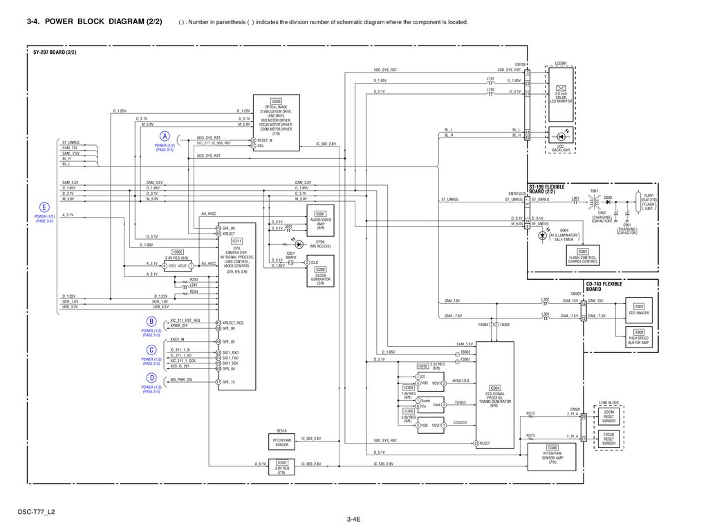
3-4. POWER BLOCK DIAGRAM (2/2)( ) : Number in parenthesis ( ) indicates the division number of schematic diagram where the component is located.
SY-207 BOARD (2/2)
D_3.1V
M_5.0V
D_3.1V
M_5.0V
A
ST_UNREG
CAM_13V
CAM_-7.5V
BL_H
BL_L
POWER (1/2)
(PAGE 3-3)
L701
D_1.85V
D_3.1V
L702
D_3.1V
BL_L
BL_H
E8 RESET_N
E7 XDL
BL_L
BL_H
3
22
3.0 inch
COLOR
LCD MONITOR
23
44
45
IC_503_2.8V
LCD
BACKLIGHT
XDD_SYS_RST
CAM_3.5V
D_1.85V
D_3.1V
M_5.0V
CAM_3.5V
D_1.85V
D_3.1V
M_5.0V
CN701(2/2)
ST_UNREG
ST_UNREG
ST-199 FLEXIBLE
BOARD (2/2)
6, 7
CAM_3.5V
D_1.85V
D_3.1V
M_5.0V
XDD_SYS_RST
XIC_211_IC_503_RST
D_1.85V
IC503
OPTICAL IMAGE
STABILIZATION DRIVE,
LENS DRIVE,
IRIS MOTOR DRIVER,
FOCUS MOTOR DRIVER,
ZOOM MOTOR DRIVER
(7/9)
D_1.25V
D_1.25V
LCD901
CN709
XDD_SYS_RST
XDD_SYS_RST
T001
E
POWER (1/2)
(PAGE 3-3)
AU_AVCC
A_3.1V
D_3.1V
D_3.1V
D_3.1V L601
IC211
D_1.85V
IC602
2.8V REG (8/9)
A_3.1V
4 VDD VOUT 1
AU_AVCC
D_3.1V
D_1.85V
(
D_3.1V
D_3.1V
14
M_5.0V
AF_ANODE
8
AUDIO/VIDEO
AMP
(8/9)
IC001
2 ICLK
IC202
CLOCK
GENERATOR
(2/9)
CD-743 FLEXIBLE
BOARD
CN301
D_1.25V
DDR_1.8V
USB_3.2V
XIC_211_RST_REQ
XPWR_OFF
POWER (1/2)
(PAGE 3-3)
POWER (1/2)
(PAGE 3-3)
D
CAM_13V
L302
CAM_-7.5V
L301
W12 XRESET_REQ
G8 GPE_00
FB304
CAM_13V
CAM_-7.5V
14
12
CAM_13V
IC001
CAM_-7.5V
CCD IMAGER
FB303
IC002
XACV_IN
C
CHARGING
(CAPACITOR
)
FLASH CONTROL,
CHARGE CONTROL
R254
B
+
C901
X201
38MHz
R253
L241
D_1.25V
DDR_1.8V
USB_3.2V
+
)
D004
AF ILLUMINATOR/
SELF-TIMER
D706
(MS ACCESS)
CPU,
CAMERA DSP,
AV SIGNAL PROCESS,
LENS CONTROL,
MODE CONTROL
(3/9, 4/9, 5/9)
A_3.1V
C902
CHARGING
CAPACITOR
IC601
H10 GPE_09
AB18 XRESET
FL001
(FL61210)
FLASH
UNIT
D003
L001
ST_UNREG
IC_211_1_SI
IC_211_1_SO
XIC_211_1_SCK
XCS_IC_201
MS_PWR_ON
K8 GPE_05
HIGH SPEED
BUFFER AMP
CAM_3.5V
FB302
D_1.85V
G18 SIO1_RXD
B24 SIO1_TXD
H18 SIO1_SCK
W20 GPS_04
FB301
D_3.1V
IC302 2.3V REG
(6/9)
1 CE
T7 GPE_15
4 VDD
POWER (1/2)
(PAGE 3-3)
VOUT 3
HVDD1/2/3
IC303
IC304
1.8V REG
(6/9)
CCD SIGNAL
PROCESS,
TIMING GENERATOR
(6/9)
1 Vcont
6 Vin
Vout 4
TGVDD
IC305
2.8V REG
(6/9)
4 VDD
VOUT 1
LENS BLOCK
R572
CN501
Z_PI_A
R573
F_PI_A
29
ZOOM
RESET
SENSOR
21
FOCUS
RESET
SENSOR
CCDVDD
SE510
PITCH/YAW
SENSOR
IC_503_2.8V
XDD_SYS_RST
D_3.1V
A_3.1V
IC507
2.8V REG
(7/9)
IC_503_2.8V
IC_503_2.8V
DSC-T77_L2
3-4E
E3 RESET
IC506
PITCH/YAW
SENSOR AMP
(7/9)
33.
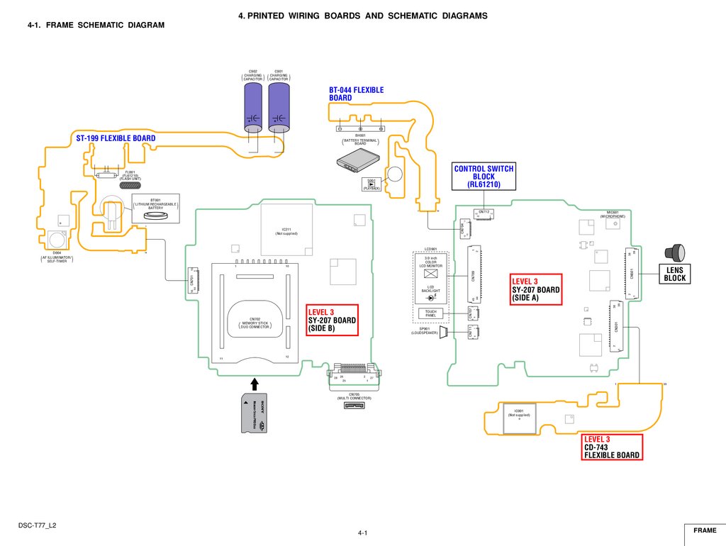
4. PRINTED WIRING BOARDS AND SCHEMATIC DIAGRAMS4-1. FRAME SCHEMATIC DIAGRAM
C902
C901
CHARGING
CHARGING
( CAPACITOR
) ( CAPACITOR
)
BT-044 FLEXIBLE
BOARD
BH001
BATTERY TERMINAL
BOARD
ST-199 FLEXIBLE BOARD
FL001
(FL61210)
(FLASH UNIT)
CONTROL SWITCH
BLOCK
(RL61210)
S001
(PLAYBACK)
BT001
RECHARGEABLE
( LITHIUMBATTERY
)
1
10
CN712 11
MIC601
(MICROPHONE)
1
IC211
(Not supplied)
38
14
)
2
1
6
SP901
(LOUDSPEAKER)
1
2
8
6
1
7
CN301
8
TOUCH
PANEL
CN707
LEVEL 3
SY-207 BOARD
(SIDE B)
CN702
MEMORY STICK
DUO CONNECTOR
CN711
7
38
45
44
LEVEL 3
SY-207 BOARD
(SIDE A)
LENS
BLOCK
1
CN709
16
CN701
14
LCD
BACKLIGHT
CN501
3.0 inch
COLOR
LCD MONITOR
10
15
1
1
39
(
1
2
LCD901
D004
AF ILLUMINATOR/
SELF-TIMER
39
CN704
1
12
10
11
1
12
10
11
12
28
26
25
2
27
1
1
39
CN705
(MULTI CONNECTOR)
IC001
(Not supplied)
LEVEL 3
CD-743
FLEXIBLE BOARD
DSC-T77_L2
4-1
FRAME
34.
4-2. SCHEMATIC DIAGRAMSLink
ST-199 FLEXIBLE BOARD
(FLASH DRIVE)
BT-044 FLEXIBLE BOARD
(BATTERY IN/PLAYBACK SWITCH)
COMMON NOTE FOR SCHEMATIC DIAGRAMS
DSC-T77_L2
CONTROL SWITCH BLOCK
(RL61210)
35.
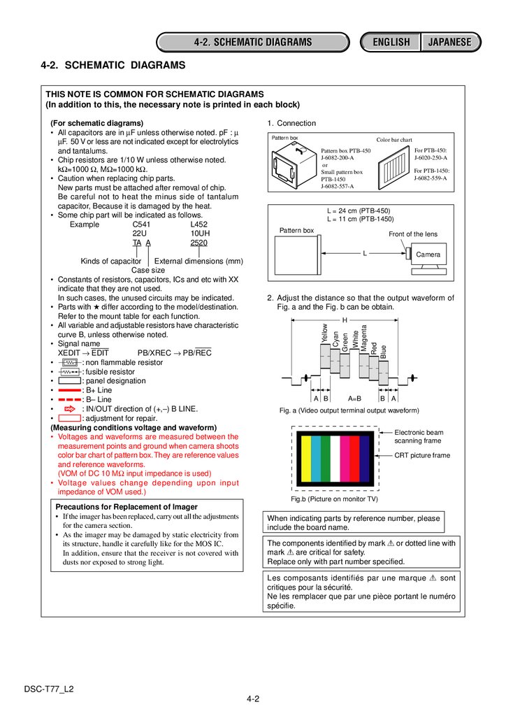
ENGLISH4-2. SCHEMATIC DIAGRAMS
JAPANESE
4-2. SCHEMATIC DIAGRAMS
THIS NOTE IS COMMON FOR SCHEMATIC DIAGRAMS
(In addition to this, the necessary note is printed in each block)
(For schematic diagrams)
• All capacitors are in µF unless otherwise noted. pF : µ
µF. 50 V or less are not indicated except for electrolytics
and tantalums.
• Chip resistors are 1/10 W unless otherwise noted.
kΩ=1000 Ω, MΩ=1000 kΩ.
• Caution when replacing chip parts.
New parts must be attached after removal of chip.
Be careful not to heat the minus side of tantalum
capacitor, Because it is damaged by the heat.
• Some chip part will be indicated as follows.
Example
C541
L452
22U
10UH
TA A
2520
1. Connection
Pattern box
Color bar chart
For PTB-450:
J-6020-250-A
Pattern box PTB-450
J-6082-200-A
or
Small pattern box
PTB-1450
J-6082-557-A
For PTB-1450:
J-6082-559-A
L = 24 cm (PTB-450)
L = 11 cm (PTB-1450)
Pattern box
Front of the lens
L
Kinds of capacitor
External dimensions (mm)
Case size
• Constants of resistors, capacitors, ICs and etc with XX
indicate that they are not used.
In such cases, the unused circuits may be indicated.
• Parts with ★ differ according to the model/destination.
Refer to the mount table for each function.
• All variable and adjustable resistors have characteristic
curve B, unless otherwise noted.
• Signal name
XEDIT → EDIT
PB/XREC → PB/REC
• 2: non flammable resistor
• 5: fusible resistor
• C: panel designation
• A: B+ Line
• B: B– Line
• J : IN/OUT direction of (+,–) B LINE.
• C: adjustment for repair.
(Measuring conditions voltage and waveform)
• Voltages and waveforms are measured between the
measurement points and ground when camera shoots
color bar chart of pattern box. They are reference values
and reference waveforms.
(VOM of DC 10 MΩ input impedance is used)
• Voltage values change depending upon input
impedance of VOM used.)
Camera
A B
Red
Blue
White
Magenta
H
Cyan
Green
Yellow
2. Adjust the distance so that the output waveform of
Fig. a and the Fig. b can be obtain.
A=B
B A
Fig. a (Video output terminal output waveform)
Electronic beam
scanning frame
CRT picture frame
Fig.b (Picture on monitor TV)
Precautions for Replacement of Imager
• If the imager has been replaced, carry out all the adjustments
for the camera section.
• As the imager may be damaged by static electricity from
its structure, handle it carefully like for the MOS IC.
In addition, ensure that the receiver is not covered with
dusts nor exposed to strong light.
When indicating parts by reference number, please
include the board name.
The components identified by mark 0 or dotted line with
mark 0 are critical for safety.
Replace only with part number specified.
Les composants identifiés par une marque 0 sont
critiques pour la sécurité.
Ne les remplacer que par une pièce portant le numéro
spécifie.
DSC-T77_L2
4-2
36.
ENGLISH4-2. SCHEMATIC DIAGRAMS
JAPANESE
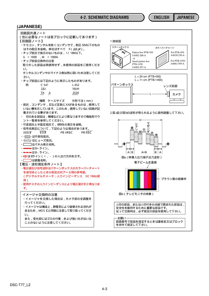
(JAPANESE)
回路図共通ノート
他に必要なノートは各ブロックに記載してあります
【回路図ノート】
1. 接続図
・ケミコン タンタルを除くコンデンサで 耐圧50V以下のもの
はその耐圧を省略。単位はすべてμF pはpF 。
・チップ抵抗で指示のないものは 1 10W以下。
kΩ 1000Ω MΩ 1000kΩ
・チップ部品交換時の注意
取り外した部品は再使用せず 未使用の部品をご使用くださ
い。
タンタルコンデンサのマイナス側は熱に弱いため注意してくだ
さい。
・チップ部品には下記のように表示したものがあります。
例
C 541
L 452
22U
10UH
TA
A
2520
↑ ↑
↑
種類 ケースサイズ
外形寸法 mm
・抵抗 コンデンサ ICなど定数にXXがあるものは 使用して
いない事を示しています。このため 使用していない回路が記
載されている事があります。
・★印のある部品は 機種などにより異なりますので機能別マウ
ント一覧表を参照してください。
・可変抵抗と半固定抵抗で B特性の表示を省略。
・信号名表記について 下記のような場合があります。
XEDIT → EDIT
PB/XREC → PB/REC
・2は不燃性抵抗。
・1はヒューズ抵抗。
・Cはパネル表示名称。
・AはB ライン。
・BはB−ライン。
・JはBライン − の入出力方向を示す。
・Cは調整名称。
パターンボックス
カラーバーチャート
For PTB-450:
J-6020-250-A
Pattern box PTB-450
J-6082-200-A
or
Small pattern box
PTB-1450
J-6082-557-A
For PTB-1450:
J-6082-559-A
L = 24 cm (PTB-450)
L = 11 cm (PTB-1450)
パターンボックス
レンズ前面
L
カメラ
2. 図a及び図bの波形が得られるように画枠調整して下さい。
H
シ
黄 ア
ン
A B
マ
ゼ
白 ン
緑
ダ 赤
A=B
青
B A
図a 映像入出力端子出力波形
電子ビーム走査線
【電圧・波形測定条件ノート】
・電圧値及び信号波形はパターンボックスのカラーバーチャート
を被写体としたときの測定点対アース間の参考値。
デジタルマルチメータ 入力インピーダンス DC10MΩ使
用
・使用テスタの入力インピーダンスにより電圧値が多少異なりま
す。
ブラウン管の画像枠
図b テレビモニタの映像
イメージャ交換時の注意
・イメージャを交換した場合は カメラ部の全調整を
行ってください。
・イメージャは構造上 静電気により破壊される恐れが
あるため MOS ICと同様に注意して取り扱ってくださ
い。
また 受光部にはゴミの付着 および強い光がはいる
ことのないように注意してください。
0印の部品 または0印付きの点線で囲まれた部品は
安全性を維持するために重要な部品です。
従って交換時は 必ず指定の部品を使用して下さい。
お願い
図面番号で部品を指定するときは基板名又はブロック
を併せて指定して下さい。
DSC-T77_L2
4-3
37.
Schematic diagrams of the CD-743 flexible board and SY-207 board are not shown.Pages from 4-4 to 4-13 are not shown.
DSC-T77_L2
38.
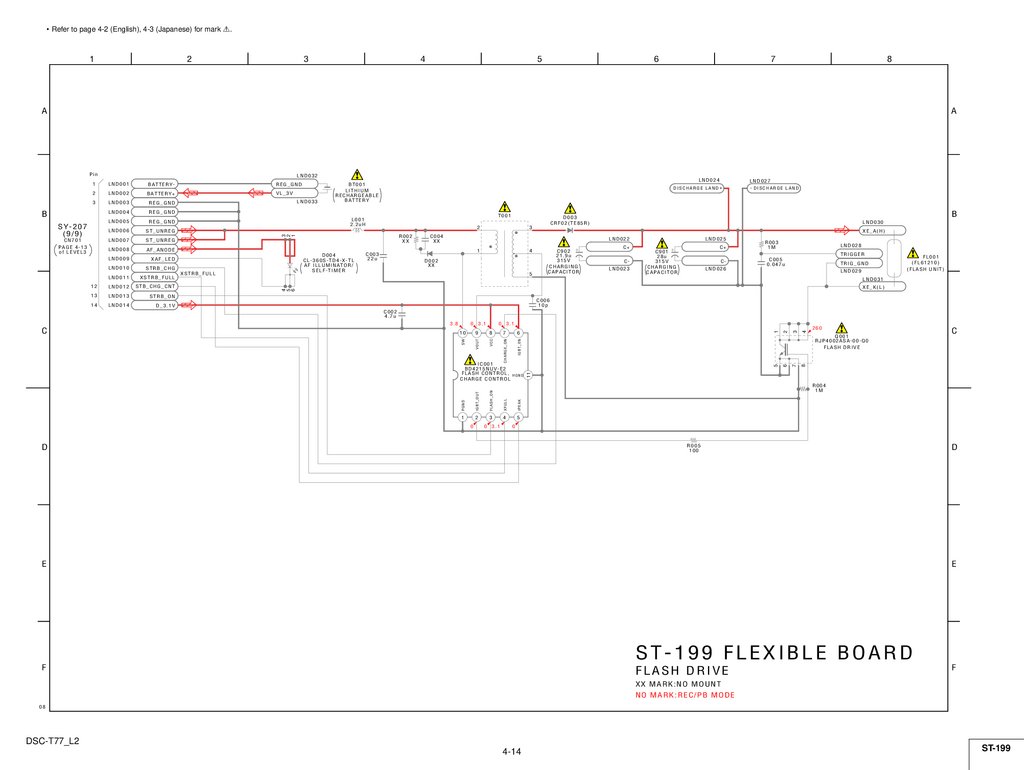
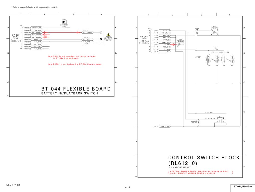
• Refer to page 4-2 (English), 4-3 (Japanese) for mark 0.2
1
4
3
5
6
7
8
A
A
Pin
LND032
1
LND001
BATTERY-
REG_GND
2
LND002
BATTERY+
VL_3V
3
LND003
REG_GND
LND004
REG_GND
LND005
REG_GND
B
LND006
ST_UNREG
LND007
ST_UNREG
LND008
AF_ANODE
T001
L001
2.2uH
2
LND009
XAF_LED
LND010
STRB_CHG
LND011
XSTRB_FULL
12
LND012
STB_CHG_CNT
13
LND013
STRB_ON
14
LND014
D_3.1V
R002
XX
D004
CL-360S-TD4-X-TL
AF ILLUMINATOR/
SELF-TIMER
XSTRB_FULL
B
D003
CRF02(TE85R)
3
LND030
XE_A(H)
C004
XX
LND025
LND022
1
C003
22u
4
D002
XX
5
- DISCHARGE LAND
C902
21.9u
315V
CHARGING
CAPACITOR
C+
C+
CLND023
C901
28u
315V
CHARGING
CAPACITOR
R003
1M
LND028
TRIGGER
CLND026
C005
0.047u
TRIG_GND
LND029
FL001
(FL61210)
(FLASH UNIT)
LND031
XE_K(L)
4
5
6
CN701
PAGE 4-13
of LEVEL3
LND027
DISCHARGE LAND+
3
2
1
SY-207
(9/9)
LND033
LND024
BT001
LITHIUM
RECHARGEABLE
BATTERY
C006
10p
C002
4.7u
4
2
3
8
7
IGBT_EN
4
IPEAK
3
0 3.1
1
CHARGE_ON
2
0
XFULL
1
C
R004
1M
FLASH_ON
PGND
IGBT_OUT
IC001
BD4215NUV-E2
F L A S H C O N T R O L , HGND
CHARGE CONTROL
260
Q001
RJP4002ASA-00-Q0
FLASH DRIVE
6
6
5
7
11
8
VCC
0 3.1
9
VOUT
0 3.1
10
SW
3.8
C
5
0
R005
100
D
E
D
E
ST-199 FLEXIBLE BOARD
F
FLASH DRIVE
F
XX MARK:NO MOUNT
NO MARK:REC/PB MODE
08
DSC-T77_L2
4-14
ST-199
39.
• Refer to page 4-2 (English), 4-3 (Japanese) for mark 0.1
3
2
4
1
3
2
4
S001
(PLAYBACK)
SW_GND
3
LND003
BATT_UNREG
LND004
BATT_UNREG
SY-207
(9/9)
LND011
BATT_UNREG
LND005
BATT_UNREG
LND006
BATT_SIG
BATT_SIG
LND007
BATT_GND
BATT_GND
8
LND008
BATT_GND
LND013
9
LND009
BATT_GND
10
LND010
BATT_GND
LND012
CN704
PAGE 4-13
of LEVEL3
s
B
1
LND001
XAE_LOCK_SW
2
LND002
XSHUT_SW
3
LND003
REG_GND
SY-207
(9/9)
BH001
BATTERY
TERMINAL
BOARD
CN712
PAGE 4-13
of LEVEL3
B
S002
POWER
D003
XX
Pin
LND004
REG_GND
LND005
XPWR_ON
LND006
XPWR_LED
LND007
D_3.1V
8
LND008
REG_GND
9
LND009
KEY_AD1
10
LND010
N.C.
A
2
1
4
3
D001
650103001
(POWER)
R001
2200
T
B
Note:S001 is not supplied, but this is included
in BT-044 flexible board.
D002
XX
(ZOOM)
W
B
REG_GND
LND014
LND002
A
LND013
2
A
XZOOM_W
XDIRECT_PB
REG_GND
LND012
LND001
LND011
1
XZOOM_T
Pin
A
Note:BH001 is not included in BT-044 flexible board.
C
C
C
C
BT-044 FLEXIBLE BOARD
BATTERY IN/PLAYBACK SWITCH
08
D
D
XSHUT_SW
S001
(SHUTTER)
1
4
3
2
XAE_LOCK_SW
D004
XX
3
1
2
LND015
STATIC_GND
E
E
CONTROL SWITCH BLOCK
(RL61210)
F
XX MARK:NO MOUNT
F
CONTROL SWITCH BLOCK(RL61210) is replaced as block,
so that PRINTED WIRING BOARD is omitted.
08
DSC-T77_L2
4-15
BT-044, RL61210
40.
4-3. PRINTED WIRING BOARDSLink
ST-199 FLEXIBLE BOARD
COMMON NOTE FOR PRINTED WIRING BOARDS
DSC-T77_L2
BT-044 FLEXIBLE BOARD
41.
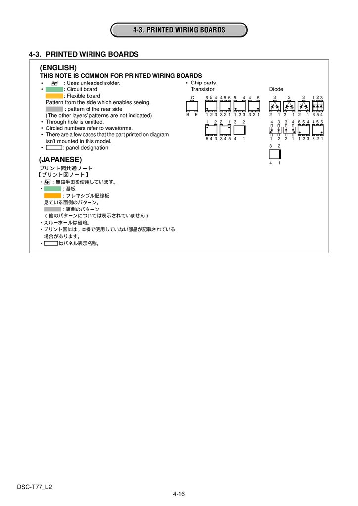
4-3. PRINTED WIRING BOARDS4-3. PRINTED WIRING BOARDS
(ENGLISH)
THIS NOTE IS COMMON FOR PRINTED WIRING BOARDS
• Chip parts.
Transistor
: Uses unleaded solder.
: Circuit board
: Flexible board
Pattern from the side which enables seeing.
: pattern of the rear side
(The other layers’ patterns are not indicated)
• Through hole is omitted.
• Circled numbers refer to waveforms.
• There are a few cases that the part printed on diagram
isn’t mounted in this model.
• C: panel designation
6 5 4 4 5 6 5
C
B
(JAPANESE)
プリント図共通ノート
【プリント図ノート】
・
・
無鉛半田を使用しています。
基板
フレキシブル配線板
見ている面側のパターン。
裏側のパターン
他のパターンについては表示されていません
・スルーホールは省略。
・プリント図には 本機で使用していない部品が記載されている
場合があります。
・Cはパネル表示名称。
DSC-T77_L2
4-16
Diode
E
4 4
3
5
3
3
1 23
1 2 3 3 2 1 1 2 3 3 2 1
2
1 2
1 2
1
4
3
3
4 6 5 4 4 5 6
2
1 1 2 3 3 2 1
2 2
1 3
2
5 4 3 3 4 5 4
1
1
2
3
2
4
1
1 6 54
42.
Printed wiring boards of the CD-743 flexible board and SY-207 board are not shown.Pages from 4-17 to 4-19 are not shown.
DSC-T77_L2
43.
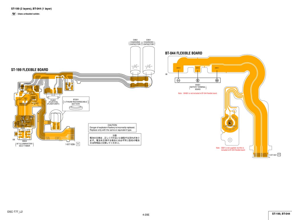
ST-199 (2 layers), BT-044 (1 layer): Uses unleaded solder.
(
C902
CHARGING
CAPACITOR
)(
C901
CHARGING
CAPACITOR
)
BT-044 FLEXIBLE BOARD
LND013
ST-199 FLEXIBLE BOARD
LND012
LND011
R004
4
2
LND030
LND028
LND029
)
BT001
RECHARGEABLE )
( LITHIUMBATTERY
C002
S001
C004
1
5
6
4
1
D004
AF ILLUMINATOR/
SELF-TIMER
-
+
LND033
11
3
(
(
BH001
BATTERY TERMINAL
BOARD
Note : BH001 is not included in BT-044 flexible board.
R002 10
6
IC001
R005
08
FL001
(FL61210)
(FLASH UNIT)
LND032
300C
C006
D002
LND031
1
L001
T001
1
LND025
5
C005
A
3
LND026
4
Q001
300D
8
5
R003
LND022
LND024
K
LND023
LND027
08
1
LND001
LND002
LND003
LND004
LND005
LND006
LND007
LND008
LND009
LND010
LND011
LND012
LND013
LND014
14
)
1-877-836- 11
CAUTION
Danger of explosion if battery is incorrectly replaced.
Replace only with the same or equivalent type.
(PLAYBACK)
注意
電池の交換は 正しく行わないと破裂する恐れがあり
ます。電池を交換する場合には必ず同じ型名の電池
又は同等品と交換してください。
1
DSC-T77_L2
4-20E
LND001
LND002
LND003
LND004
LND005
LND006
LND007
LND008
LND009
LND010
Note : S001 is not supplied, but this is
included in BT-044 flexible board.
1-877-837- 11
10
ST-199, BT-044
44.
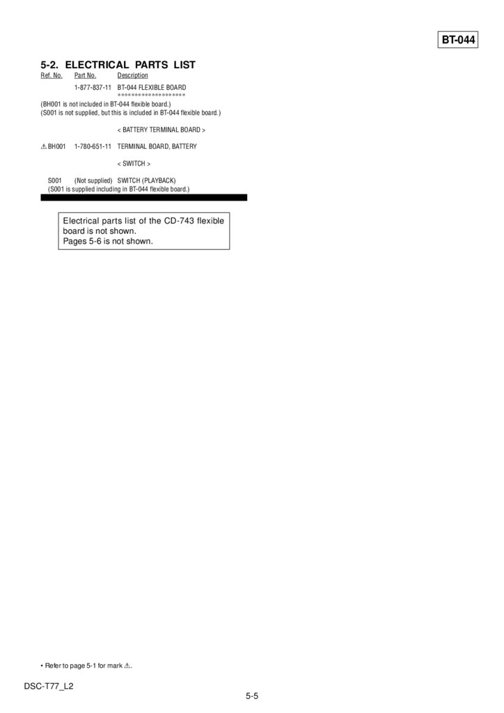
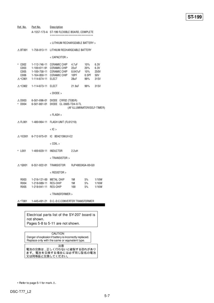
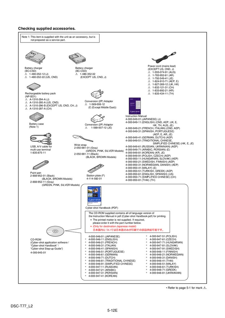
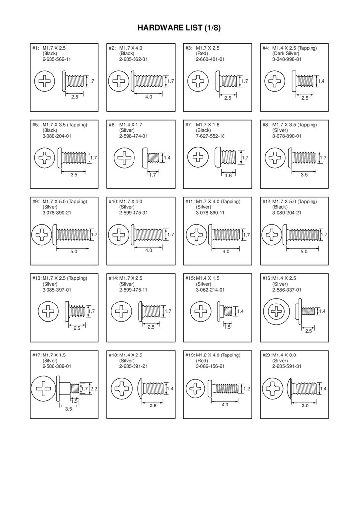
NOTE5. REPAIR PARTS LIST
NOTE: Characters A to Z of the electrical parts list indicate location of exploded views in which the desired part is shown.
EXPLODED VIEWS
Link
A
B
OVERALL SECTION
Link
BT-044 FLEXIBLE BOARD
DSC-T77_L2
C
ST/REAR SECTION
MAIN SECTION
ELECTRICAL PARTS LIST
C
ST-199 FLEXIBLE BOARD
C
ACCESSORIES
45.
5. REPAIR PARTS LIST5. REPAIR PARTS LIST
(ENGLISH)
NOTE:
• -XX, -X mean standardized parts, so they may have some differences from
the original one.
• Items marked “*” are not stocked since they are seldom required for routine
service. Some delay should be anticipated when ordering these items.
• The mechanical parts with no reference number in the exploded views are not
supplied.
• Due to standardization, replacements in the parts list may be different from
the parts specified in the diagrams or the components used on the set.
• CAPACITORS:
uF: µF
• COILS
uH: µH
• RESISTORS
All resistors are in ohms.
METAL: metal-film resistor
METAL OXIDE: Metal Oxide-film resistor
F: nonflammable
• SEMICONDUCTORS
In each case, u: µ, for example:
uA...: µA... , uPA... , µPA... ,
uPB... , µPB... , µPC... , µPC... ,
uPD..., µPD...
When indicating parts by reference number,
please include the board name.
The components identified by mark 0 or
dotted line with mark 0 are critical for safety.
Replace only with part number specified.
Les composants identifiés par une marque
0 sont critiques pour la sécurité.
Ne les remplacer que par une pièce portant
le numéro spécifié.
• Color Indication of Appearance Parts
Example:
(SILVER) : Cabinet’s Color
(Silver) : Parts Color
(JAPANESE)
【使用上の注意】
• ここに記載されている部品は, 補修用部品であるため, 回路図及び
セットに付いている部品と異なる場合があります。
• -XX, -Xは標準化部品のため, セットに付いている部品と異なる場合
があります。
• *印の部品は常備在庫しておりません。
• コンデンサの単位でuFはμFを示します。
• 抵抗の単位Ωは省略してあります。
金
被 金属被膜抵抗。
サンキン 酸化金属被膜抵抗。
• インダクタの単位でuHはμHを示します。
• 半導体の名称でuA..., uPA..., uPB..., uPC..., uPD...等はそれぞれμ
A..., μPA..., μPB..., μPC..., μPD...を示します。
• Abbreviation
AR : Argentine model
AUS : Australian model
BR : Brazilian model
CH : Chinese model
CND : Canadian model
EE : East European model
HK : Hong Kong model
J
: Japanese model
JE : Tourist model
KR : Korea model
NE : North European model
TH : Thai model
TW : Taiwan model
お願い
図面番号で部品を指定するときは基板名又はブロック
を併せて指定してください。
0印の部品 または0印付の点線で囲まれた部品は
安全性を維持するために 重要な部品です。
従って交換時は 必ず指定の部品を使用してください。
THE COMBINATION OF CABINET’S COLOR
AND SCREW
The screw pointed
is different according to the cabinet's color.
For the combination of cabinet's color and screw, please refer to Table 5-1.
DSC-T77_L2
5-1
Table 5-1
Screw's
Ref. No. (Parts Color.)
Cabinet's Color
#142 (Silver)
SILVER/GREEN/PINK
#143 (Black)
BLACK/BROWN
46.
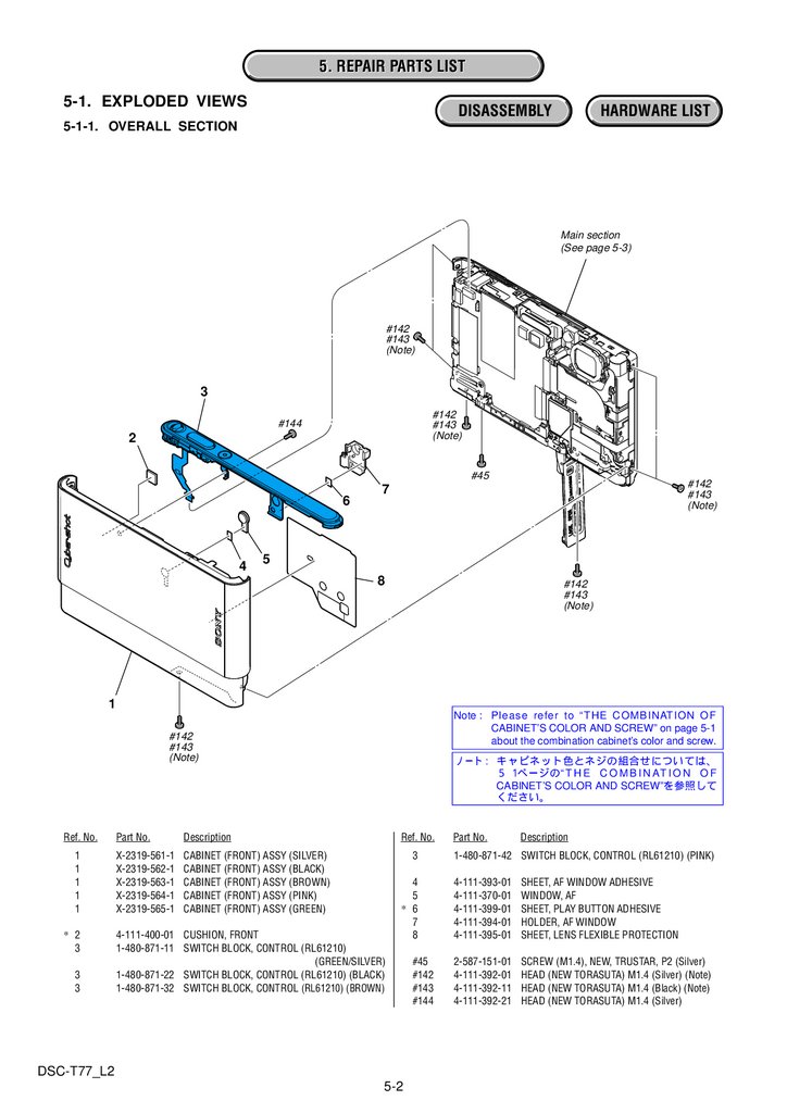
5. REPAIR PARTS LIST5-1. EXPLODED VIEWS
DISASSEMBLY
HARDWARE LIST
5-1-1. OVERALL SECTION
Main section
(See page 5-3)
#142
#143
(Note)
3
#142
#143
(Note)
#144
2
#45
6
4
#142
#143
(Note)
7
5
8
#142
#143
(Note)
1
Note : Please refer to “THE COMBINATION OF
CABINET’S COLOR AND SCREW” on page 5-1
about the combination cabinet’s color and screw.
#142
#143
(Note)
Ref. No.
1
1
1
1
1
* 2
3
3
3
Part No.
Description
X-2319-561-1
X-2319-562-1
X-2319-563-1
X-2319-564-1
X-2319-565-1
CABINET (FRONT) ASSY (SILVER)
CABINET (FRONT) ASSY (BLACK)
CABINET (FRONT) ASSY (BROWN)
CABINET (FRONT) ASSY (PINK)
CABINET (FRONT) ASSY (GREEN)
ノート : キャビネット色とネジの組合せについては、
5 - 1 ページの“ T H E C O M B I N AT I O N O F
CABINET’S COLOR AND SCREW”を参照して
ください。
Ref. No.
3
4-111-400-01 CUSHION, FRONT
1-480-871-11 SWITCH BLOCK, CONTROL (RL61210)
(GREEN/SILVER)
1-480-871-22 SWITCH BLOCK, CONTROL (RL61210) (BLACK)
1-480-871-32 SWITCH BLOCK, CONTROL (RL61210) (BROWN)
4
5
* 6
7
8
DSC-T77_L2
5-2
#45
#142
#143
#144
Part No.
Description
1-480-871-42 SWITCH BLOCK, CONTROL (RL61210) (PINK)
4-111-393-01
4-111-370-01
4-111-399-01
4-111-394-01
4-111-395-01
SHEET, AF WINDOW ADHESIVE
WINDOW, AF
SHEET, PLAY BUTTON ADHESIVE
HOLDER, AF WINDOW
SHEET, LENS FLEXIBLE PROTECTION
2-587-151-01
4-111-392-01
4-111-392-11
4-111-392-21
SCREW (M1.4), NEW, TRUSTAR, P2 (Silver)
HEAD (NEW TORASUTA) M1.4 (Silver) (Note)
HEAD (NEW TORASUTA) M1.4 (Black) (Note)
HEAD (NEW TORASUTA) M1.4 (Silver)
47.
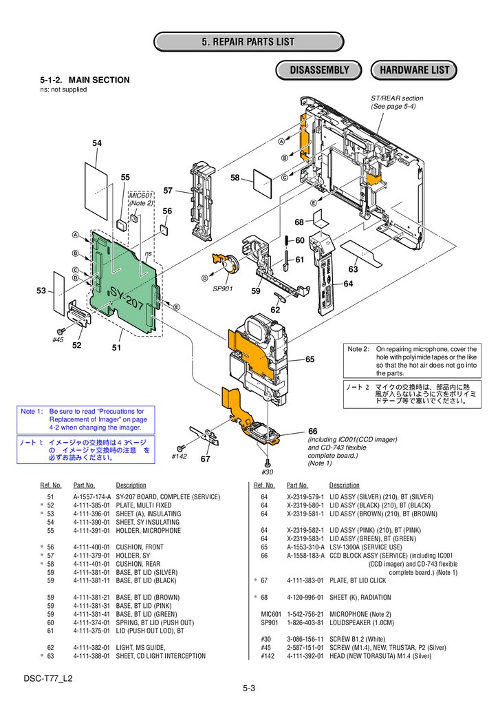
5. REPAIR PARTS LISTDISASSEMBLY
HARDWARE LIST
5-1-2. MAIN SECTION
ns: not supplied
ST/REAR section
(See page 5-4)
54
A
B
55
58
MIC601
(Note 2)
C
57
E
56
68
A
60
ns
B
61
63
C
D
D
SY
-20
53
SP901
7
#45
52
64
59
E
62
51
Note 2:
65
On repairing microphone, cover the
hole with polyimide tapes or the like
so that the hot air does not go into
the parts.
ノート 2: マイクの交換時は、部品内に熱
風が入らないように穴をポリイミ
ドテープ等で塞いでください。
Note 1:
Be sure to read “Precuations for
Replacement of Imager” on page
4-2 when changing the imager.
ノート 1: イメージャの交換時は4-3ページ
の イメージャ交換時の注意 を
必ずお読みください。
66
#142
(including IC001(CCD imager)
and CD-743 flexible
complete board.)
(Note 1)
67
#30
Ref. No.
Part No.
Description
51
* 52
* 53
54
55
A-1557-174-A
4-111-385-01
4-111-396-01
4-111-390-01
4-111-391-01
SY-207 BOARD, COMPLETE (SERVICE)
PLATE, MULTI FIXED
SHEET (A), INSULATING
SHEET, SY INSULATING
HOLDER, MICROPHONE
* 56
* 57
* 58
59
59
4-111-400-01
4-111-379-01
4-111-401-01
4-111-381-01
4-111-381-11
CUSHION, FRONT
HOLDER, SY
CUSHION, REAR
BASE, BT LID (SILVER)
BASE, BT LID (BLACK)
59
59
59
60
61
4-111-381-21
4-111-381-31
4-111-381-41
4-111-374-01
4-111-375-01
BASE, BT LID (BROWN)
BASE, BT LID (PINK)
BASE, BT LID (GREEN)
SPRING, BT LID (PUSH OUT)
LID (PUSH OUT LOD), BT
62
* 63
Ref. No.
Part No.
Description
64
64
64
X-2319-579-1 LID ASSY (SILVER) (210), BT (SILVER)
X-2319-580-1 LID ASSY (BLACK) (210), BT (BLACK)
X-2319-581-1 LID ASSY (BROWN) (210), BT (BROWN)
64
64
65
66
X-2319-582-1
X-2319-583-1
A-1553-310-A
A-1558-183-A
* 67
LID ASSY (PINK) (210), BT (PINK)
LID ASSY (GREEN), BT (GREEN)
LSV-1300A (SERVICE USE)
CCD BLOCK ASSY (SERVICE) (including IC001
(CCD imager) and CD-743 flexible
complete board.) (Note 1)
4-111-383-01 PLATE, BT LID CLICK
* 68
4-120-996-01 SHEET (K), RADIATION
MIC601 1-542-756-21 MICROPHONE (Note 2)
SP901 1-826-403-81 LOUDSPEAKER (1.0CM)
#30
#45
#142
4-111-382-01 LIGHT, MS GUIDE,
4-111-388-01 SHEET, CD LIGHT INTERCEPTION
DSC-T77_L2
5-3
3-086-156-11 SCREW B1.2 (White)
2-587-151-01 SCREW (M1.4), NEW, TRUSTAR, P2 (Silver)
4-111-392-01 HEAD (NEW TORASUTA) M1.4 (Silver)
48.
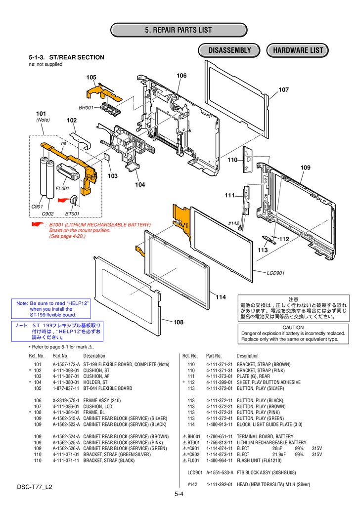
5. REPAIR PARTS LISTDISASSEMBLY
HARDWARE LIST
5-1-3. ST/REAR SECTION
ns: not supplied
106
105
107
BH001
101
(Note)
102
ns
110
109
103
104
FL001
111
C901
C902
BT001
! : BT001
(LITHIUM RECHARGEABLE BATTERY)
Board on the mount position.
#142
(See page 4-20.)
112
113
LCD901
114
Note: Be sure to read “HELP12”
when you install the
ST-199 flexible board.
ノート: S T - 1 9 9 フレキシブル基板取り
付け時は “H E L P 1 2 ”を必ずお
読みください。
注意
電池の交換は 正しく行わないと破裂する恐れ
があります。電池を交換する場合には必ず同じ
型名の電池又は同等品と交換してください。
108
CAUTION
Danger of explosion if battery is incorrectly replaced.
Replace only with the same or equivalent type.
• Refer to page 5-1 for mark 0.
Ref. No.
Part No.
Description
Ref. No.
Part No.
Description
101
* 102
103
* 104
105
A-1557-173-A
4-111-398-01
4-111-387-01
4-111-380-01
1-877-837-11
ST-199 FLEXIBLE BOARD, COMPLETE (Note)
CUSHION, ST
CUSHION, AF
HOLDER, ST
BT-044 FLEXIBLE BOARD
110
110
111
* 112
113
4-111-371-21
4-111-371-31
4-111-373-01
4-111-399-01
4-111-372-01
BRACKET, STRAP (BROWN)
BRACKET, STRAP (PINK)
PLATE (G), REAR
SHEET, PLAY BUTTON ADHESIVE
BUTTON, PLAY (SILVER)
106
107
* 108
109
109
X-2319-578-1
4-111-386-01
4-111-384-01
A-1562-515-A
A-1562-523-A
FRAME ASSY (210)
CUSHION, LCD
FRAME, BL
CABINET REAR BLOCK (SERVICE) (SILVER)
CABINET REAR BLOCK (SERVICE) (BLACK)
113
113
113
113
114
4-111-372-11
4-111-372-21
4-111-372-31
4-111-372-41
1-480-913-11
BUTTON, PLAY (BLACK)
BUTTON, PLAY (BROWN)
BUTTON, PLAY (PINK)
BUTTON, PLAY (GREEN)
BLOCK, LIGHT GUIDE PLATE (3.0)
109
109
109
110
110
A-1562-524-A
A-1562-525-A
A-1562-526-A
4-111-371-01
4-111-371-11
CABINET REAR BLOCK (SERVICE) (BROWN)
CABINET REAR BLOCK (SERVICE) (PINK)
CABINET REAR BLOCK (SERVICE) (GREEN)
BRACKET, STRAP (GREEN/SILVER)
BRACKET, STRAP (BLACK)
0 BH001
0 BT001
0*C901
0*C902
0 FL001
1-780-651-11
1-756-813-11
1-114-874-11
1-114-873-11
1-480-964-11
TERMINAL BOARD, BATTERY
LITHIUM RECHARGEABLE BATTERY
ELECT
28uF
99%
ELECT
21.9uF
99%
FLASH UNIT (FL61210)
LCD901 A-1551-533-A FTS BLOCK ASSY (30SHGU08)
#142
DSC-T77_L2
5-4
4-111-392-01 HEAD (NEW TORASUTA) M1.4 (Silver)
315V
315V
49.
BT-0445-2. ELECTRICAL PARTS LIST
Ref. No.
Part No.
Description
Ref. No.
1-877-837-11 BT-044 FLEXIBLE BOARD
********************
(BH001 is not included in BT-044 flexible board.)
(S001 is not supplied, but this is included in BT-044 flexible board.)
< BATTERY TERMINAL BOARD >
0 BH001
1-780-651-11 TERMINAL BOARD, BATTERY
< SWITCH >
S001
(Not supplied) SWITCH (PLAYBACK)
(S001 is supplied including in BT-044 flexible board.)
************************************************************
Electrical parts list of the CD-743 flexible
board is not shown.
Pages 5-6 is not shown.
• Refer to page 5-1 for mark 0.
DSC-T77_L2
5-5
Part No.
Description
50.
ST-199Ref. No.
Part No.
Description
Ref. No.
A-1557-173-A ST-199 FLEXIBLE BOARD, COMPLETE
******************************
< LITHIUM RECHARGEABLE BATTERY >
0 BT001
1-756-813-11 LITHIUM RECHARGEABLE BATTERY
< CAPACITOR >
* C002
C003
C005
C006
0*C901
1-112-746-11
1-100-611-91
1-100-758-11
1-164-850-11
1-114-874-11
CERAMIC CHIP
CERAMIC CHIP
CERAMIC CHIP
CERAMIC CHIP
ELECT
0*C902
1-114-873-11 ELECT
4.7uF
22uF
0.047uF
10PF
28uF
10%
20%
10%
0.5PF
99%
6.3V
6.3V
250V
50V
315V
21.9uF
99%
315V
< DIODE >
0 D003
* D004
6-501-096-01 DIODE CRF02 (TE85R)
6-501-861-01 DIODE CL-360S-TD4-X-TL
(AF ILLUMINATOR/SELF-TIMER)
< FLASH >
0 FL001
1-480-964-11 FLASH UNIT (FL61210)
< IC >
0*IC001
6-712-975-01 IC BD4215NUV-E2
< COIL >
* L001
1-400-820-11 INDUCTOR
2.2uH
< TRANSISTOR >
0*Q001
6-551-922-01 TRANSISTOR
RJP4002ASA-00-Q0
< RESISTOR >
R003
R004
R005
1-216-121-00 METAL CHIP
1-218-989-11 RES-CHIP
1-218-941-11 RES-CHIP
1M
1M
100
5%
5%
5%
1/10W
1/16W
1/16W
< TRANSFORMER >
0*T001
1-445-491-21 D.C.-D.C.CONVERTER TRANSFORMER
************************************************************
Electrical parts list of the SY-207 board is
not shown.
Pages 5-8 to 5-11 are not shown.
CAUTION
Danger of explosion if battery is incorrectly replaced.
Replace only with the same or equivalent type.
注意
電池の交換は 正しく行わないと破裂する恐れがあり
ます。電池を交換する場合には必ず同じ型名の電池
又は同等品と交換してください。
• Refer to page 5-1 for mark 0.
DSC-T77_L2
5-7
Part No.
Description
51.
Checking supplied accessories.Note 1: This item is supplied with the unit as an accessory, but is
not prepared as a service part.
Battery charger
(BC-CSD)
0 1-480-352-12 (J)
0 1-480-352-22 (US, CND)
Power cord (mains lead)
(EXCEPT US, CND, J)
0 1-555-074-91 (AUS)
0 1-783-952-61 (AR)
0 1-792-549-41 (JE)
0 1-824-910-71 (AEP, E)
0 1-827-269-12 (UK, HK)
0 1-832-121-31 (CH)
0 1-833-892-21 (KR)
0 1-835-434-11 (TH)
Battery charger
(BC-CSD)
0 1-480-352-32
(EXCEPT US, CND, J)
Rechargeable battery pack
(NP-BD1)
0 A-1310-294-A (J)
0 A-1310-295-A (US, CND)
0 A-1310-296-B (EXCEPT US, CND, CH, J)
0 A-1310-297-A (CH)
Conversion (2P) Adaptor
0 1-569-008-12
(E (Except Middle East))
Instruction Manual
4-000-949-01 (JAPANESE) (J)
4-000-949-11 (ENGLISH) (CND, AEP, UK, E,
Battery case
Conversion (2P) Adaptor
HK, TH, AUS, JE)
(Note 1)
0
1-569-007-12 (JE)
4-000-949-21 (FRENCH, ITALIAN) (CND, AEP)
4-000-949-31 (SPANISH, PORTUGUESE)
(AEP, E, AR, JE)
4-000-949-41 (GERMAN, DUTCH) (AEP)
4-000-949-51 (TRADITIONAL CHINESE,
SIMPLIFIED CHINESE) (HK, E, JE)
Wrist strap
USB, A/V cable for
4-000-949-61 (RUSSIAN, UKRAINIAN) (AEP)
2-050-981-01 (Gray)
multi-use terminal
4-000-949-71 (ARABIC, PERSIAN) (E)
(GREEN, PINK, SILVER Models)
1-835-875-11
4-000-949-81 (KOREAN) (KR, JE)
2-050-981-11 (Black)
4-000-949-91 (POLISH, CZECH) (AEP)
(BLACK, BROWN Models)
4-000-950-11 (HUNGARIAN, SLOVAK) (AEP)
4-000-950-21 (SWEDISH, FINNISH) (AEP)
4-000-950-31 (NORWEGIAN, DANISH) (AEP)
4-000-950-41 (MALAY) (E)
4-000-950-51 (TURKISH, GREEK) (AEP)
Paint pen
4-000-950-61 (ENGLISH, SPANISH) (US)
Station plate (F)
2-888-952-01 (Black)
4-000-950-71 (SIMPLIFIED CHINESE) (CH)
4-114-582-01
(BLACK, BROWN Models)
4-000-950-81 (THAI) (TH)
2-888-952-11 (Gray)
(GREEN, PINK, SILVER Models)
Cyber-shot Handbook (PDF)
The CD-ROM supplied contains all of language version of
the Instruction Manual in pdf (Cyber-shot Handbook.pdf) for printing.
The printed matter is not supplied. If required,
please order it with the part number below.
(Only for destination Japanese model)
日本国内については日本語のみが印刷での部品供給可能です。
CD-ROM
(Cyber-shot application software /
“Cyber-shot Handbook” /
“Cyber-shot Step-up Guide”)
4-000-945-01
*
*
*
*
*
*
*
*
*
*
*
*
*
4-000-946-01 (JAPANESE)
4-000-946-11 (ENGLISH)
4-000-946-21 (FRENCH)
4-000-946-31 (ITALIAN)
4-000-946-41 (SPANISH)
4-000-946-51 (PORTUGUESE)
4-000-946-61 (GERMAN)
4-000-946-71 (DUTCH)
4-000-946-81 (TRADITIONAL CHINESE)
4-000-946-91 (SIMPLIFIED CHINESE)
4-000-947-11 (RUSSIAN)
4-000-947-21 (ARABIC)
4-000-947-31 (PERSIAN)
4-000-947-41 (KOREAN)
*
*
*
*
*
*
*
*
*
*
*
*
*
4-000-947-51 (POLISH)
4-000-947-61 (CZECH)
4-000-947-71 (HUNGARIAN)
4-000-947-81 (SLOVAK)
4-000-947-91 (SWEDISH)
4-000-948-11 (FINNISH)
4-000-948-21 (NORWEGIAN)
4-000-948-31 (DANISH)
4-000-948-41 (THAI)
4-000-948-51 (MALAY)
4-000-948-61 (TURKISH)
4-000-948-71 (GREEK)
4-000-948-81 (UKRAINIAN)
• Refer to page 5-1 for mark 0.
DSC-T77_L2
5-12E
52.
HARDWARE LIST (1/8)#1: M1.7 X 2.5
(Black)
2-635-562-11
#2: M1.7 X 4.0
(Black)
2-635-562-31
#3: M1.7 X 2.5
(Red)
2-660-401-01
1.7
2.5
1.7
4.0
#5: M1.7 X 3.5 (Tapping)
(Black)
3-080-204-01
#11: M1.7 X 4.0 (Tapping)
(Silver)
3-078-890-11
1.7
1.7
4.0
#13: M1.7 X 2.5 (Tapping)
(Silver)
3-085-397-01
1.7
2.5
5.0
#16: M1.4 X 2.5
(Silver)
2-586-337-01
2.5
#19: M1.2 X 4.0 (Tapping)
(Red)
3-086-156-21
1.4
1.5
2.5
1.4
1.4
1.5
#18: M1.4 X 2.5
(Silver)
2-635-591-21
1.7 2.2
1.7
1.7
#15: M1.4 X 1.5
(Silver)
3-062-214-01
1.7
#17: M1.7 X 1.5
(Silver)
2-586-389-01
#12: M1.7 X 5.0 (Tapping)
(Black)
3-080-204-21
4.0
#14: M1.7 X 2.5
(Silver)
2-599-475-11
2.5
3.5
1.6
#10: M1.7 X 4.0
(Silver)
2-599-475-31
1.7
1.7
1.7
5.0
#8: M1.7 X 3.5 (Tapping)
(Silver)
3-078-890-01
1.4
3.5
1.4
2.5
#7: M1.7 X 1.6
(Black)
7-627-552-18
1.7
3.5
1.7
2.5
#6: M1.4 X 1.7
(Silver)
2-598-474-01
#9: M1.7 X 5.0 (Tapping)
(Silver)
3-078-890-21
#4: M1.4 X 2.5 (Tapping)
(Dark Silver)
3-348-998-81
#20: M1.4 X 3.0
(Silver)
2-635-591-31
1.4
1.2
4.0
3.0
53.
HARDWARE LIST (2/8)#21: M1.4 X 3.0
(Black)
2-662-396-21
#22: M1.7 X 5.0 (Tapping)
(Silver)
3-083-261-01
#23: M1.7 X 4.0 (Tapping)
(Black)
3-080-204-11
1.7
1.4
#25: M1.7 X 3.0
(Black)
2-635-562-21
1.7
4.0
5.0
3.0
#26: M1.4 X 2.0
(Silver)
2-635-591-11
3.0
3.0
#36: M3.0 X 6.0
(Silver)
4-886-821-11
3.0
4.0
6.0
6.0
#39: M2.6 X 5.0 (Tapping)
(Black)
7-685-791-09
#38: M3.0 X 20.0 (Tapping)
(Silver)
7-685-651-79
2.0
4.5
#35: M4.0 X 6.0 (Tapping)
(Silver)
3-975-291-02
8.0
#37: M2.0 X 6.0 (Tapping)
(Black)
3-080-206-31
3.0
4.0
#34: M3.0 X 8.0
(Black)
3-077-331-41
6.0
#32: M2.0 X 4.5 (Tapping)
(Silver)
2-102-498-01
1.2
3.5
#33: M3.0 X 6.0
(Silver)
3-077-331-21
4.0
#31: M3.0 X 4.0
(Silver)
2-102-434-01
1.4
1.4
1.4
2.0
#30: M1.2 X 3.5 (Tapping)
(White)
3-086-156-11
2.5
#28: M1.4 X 4.0 (Tapping)
(Silver)
3-348-998-61
1.4
2.0
#29: M1.4 X 2.5
(Black)
2-662-396-01
1.7
5.5
#27: M1.4 X 2.0
(Black)
2-662-396-11
1.7
3.0
#24: B1.7 X 5.5 (Tapping)
(Black)
4-679-805-11
#40: M2.0 X 4.0 (Tapping)
(Silver)
7-685-851-04
3.0
2.0
6.0
2.6
20.0
5.0
2.0
4.0
54.
HARDWARE LIST (3/8)#41: M3.0 X 8.0 (Tapping)
(Silver)
3-065-748-01
#42: M2.0 X 4.0 (Tapping)
(Silver)
7-628-253-00
#43: M1.7 X 4.0
(Red)
2-660-401-31
2.0
3.0
8.0
#46: M1.7 X 3.0
(Red)
2-660-401-11
#49: M2.0 X 4.0
(Black)
2-630-005-31
3.0
#50: M2.0 X 3.0
(Red)
2-891-494-11
2.0
4.0
#48: M1.7 X 2.5
(Silver)
3-973-497-91
1.4
1.7
3.0
1.7
3.0
#47: M1.4 X 3.0 (Tapping)
(Silver)
2-665-774-01
1.4
2.5
1.7
4.0
4.0
#45: M1.4 X 2.5
(Silver)
2-587-151-01
#44: M1.7 X 3.0 (Tapping)
(Silver)
3-078-890-61
1.7
2.5
#51: M2.0 X 2.5
(Silver)
3-073-686-01
#52: M2.0 X 4.0 (Tapping)
(Black)
3-080-206-11
2.0
2.0
2.0
4.0
3.0
2.5
#53: M2.0 X 5.0 (Tapping)
(Black)
3-080-206-21
#54: M1.75 X 6.0 (Tapping)
(Black)
3-318-203-11
6.0
5.0
#57: M1.7 X 4.0
(Black)
7-627-852-18
#56: M2.0 X 3.5
(Silver)
3-067-187-11
1.75
2.0
2.0
4.0
#58: M2.0 X 6.0 (Tapping)
(Silver)
3-719-408-11
6.0
2.0
3.5
#59: M2.0 X 5.0 (Tapping)
(Silver)
3-080-205-21
2.0
1.7
4.0
#55: M2.0 X 4.0
(Silver)
2-655-582-11
#60: M2.6 X 5.0
(Black)
3-061-062-11
2.6
2.0
5.0
5.0
55.
HARDWARE LIST (4/8)#61: M3.0 X 10.0
(Black)
7-682-549-09
#62: M2.0 X 3.0
(Silver)
3-080-202-21
3.0
10.0
2.0
12.5
#66: M1.4 X 1.4
(Silver)
2-635-591-41
1.4
3.5
#77: M1.2 X 5.0 (Tapping)
(Silver)
3-086-156-31
#72: M1.4 X 2.0
(Silver)
4-663-621-41
1.4
1.4
2.0
2.0
#75: M1.7 X 3.5 (Tapping)
(Silver)
2-666-551-01
#76: M1.7 X 4.0 (Tapping)
(Silver)
2-666-551-11
1.7
1.7
1.7
6.0
3.5
4.0
#78: M1.4 X 3.5
(Red)
3-208-537-11
#79: M1.4X 2.0
(Silver)
2-587-151-11
#80: M1.4X 2.0
(Black)
3-279-411-01
1.4
1.4
1.2
5.0
#71: M1.4 X 2.0
(Red)
3-208-537-01
#74: M1.7 X 6.0 (Tapping)
(Silver)
2-666-551-31
4.0
4.0
2.0
5.0
1.2
1.7
1.4
1.7
1.7
#73: M1.2 X 4.0 (Tapping)
(Black)
3-086-156-61
#68: M1.7 X 4.0
(Silver)
2-655-581-01
1.4
#70: M1.7 X 5.0
(Silver)
2-599-475-41
3.0
5.0
#67: M1.4 X 2.0
(Silver)
3-389-523-16
1.4
#69: M1.7 X 3.0
(Silver)
2-599-475-21
1.7
5.0
3.0
#65: M1.4 X 3.5
(Silver)
2-635-591-01
#64: M1.7 X 5.0 (Tapping)
(Silver)
2-666-551-21
#63: M5.0 X 12.5
(Black)
3-060-811-21
3.5
2.0
1.4
2.0
56.
HARDWARE LIST (5/8)#82: M1.4 X 1.4
(Silver)
3-272-251-01
#81: M1.7 X 2.5
(Silver)
2-515-756-01
1.7
1.4
2.5
#86: M1.7 X 4.0 (Tapping)
(Silver)
2-695-434-21
2.5
#97: M1.4 X 2.5
(Black)
2-662-396-31
1.4
8.0
1.4
2.5
#99: M2.5 X 6.0 (Tapping)
(Silver)
3-776-750-02
3.8
8.0
#96: M1.4 X 2.5
(Silver)
2-587-151-21
3.0
1.7
#98: M3.0 X 8.0
(Silver)
3-077-331-01
2.5
3.9
#95: M3.0 X 8.0 (Tapping)
(Black)
7-685-646-79
4.0
3.5
2.0
1.7
3.5
#94: M1.7 X 4.0
(Black)
2-515-483-31
1.7
#92: M2.0 X 3.9
(Black)
3-268-954-01
#91: M1.7 X 3.0 (Tapping)
(Silver)
2-695-434-11
3.0
1.6
5.9
1.7
2.0
#93: M1.7 X 3.5 (Tapping)
(Silver)
3-254-082-01
1.6
5.3
#90: M1.7 X 3.0
(Silver)
3-271-395-01
5.0
#88: M1.6 X 5.9 (Tapping)
(Silver)
2-689-015-01
#87: M1.6 X 5.3
(Black)
2-689-328-01
4.0
2.0
3.0
1.7
1.7
#89: M2.0 X 5.5 (Tapping)
(Silver)
2-695-575-01
1.7
7.0
1.4
#85: M1.7 X 2.5
(Black)
2-515-483-11
#84: M2.0 X 3.0
(Silver)
3-072-453-11
#83: M1.7 X 7.0 (Tapping)
(Black)
3-080-204-41
#100: M2.0 X 6.0
(Black)
3-080-203-51
2.5
6.0
2.0
6.0
57.
HARDWARE LIST (6/8)#102: M2.6 X 8.0
(Black)
7-621-284-30
#101: M2.0 X 5.0
(Silver)
7-621-555-39
2.6
2.0
5.0
#105: M2.0 X 4.0
(Red)
2-891-494-31
10.0
#106: M2.0 X 6.0
(Black)
3-713-786-11
#107: M2.0 X 5.0
(Silver)
3-032-750-01
2.0
4.0
6.0
#109: M1.7 X 3.0
(Black)
2-515-483-21
#110: M2.0 X 3.0
(Black)
2-630-005-21
5.0
#117: M1.7 X 4.5 (Tapping)
(Silver)
2-695-429-31
#112: M1.4 X 5.0
(Black)
2-178-410-11
1.4
5.0
#115: M1.4 X 3.5 (Tapping)
(Silver)
3-348-998-51
#116: M2.0 X 3.5 (Tapping)
(Silver)
2-695-435-01
2.0
1.4
3.5
#118: M1.4 X 2.0
(Black)
2-655-580-01
#119: M2.6 X 5.0
(Black)
7-627-556-58
1.4
2.0
3.0
4.0
5.5
1.7
1.7
1.7
2.0
1.7
#108: M1.7 X 3.0 (Tapping)
(Black)
2-695-430-01
#111: M1.7 X 4.0 (Tapping)
(Black)
2-887-124-01
#114: M2.0 X 5.5 (Tapping)
(Silver)
2-698-464-01
#113: M1.7 X 5.0
(Black)
2-635-562-41
8.0
5.0
3.0
3.0
3.0
2.0
2.0
1.7
#104: M3.0 X 8.0
(Black)
7-682-548-09
2.6
8.0
2.0
4.5
#103: M2.6 X 10.0
(Silver)
7-685-794-09
3.5
#120: M2.6 X 6.0
(Silver)
7-621-770-67
2.6
2.6
5.0
6.0
58.
HARDWARE LIST (7/8)#122: M3.0 X 6.0
(Black)
7-682-547-09
#121: M2.0 X 4.0 (Tapping)
(Silver)
3-080-205-11
#123: M4.0 X 8.0
(Black)
7-682-561-09
3.0
2.0
#124: M1.7 X 2.0
(Silver)
2-599-475-01
4.0
1.7
4.0
6.0
8.0
2.0
#125: M1.4 X 3.0
(Black)
3-291-847-01
#126: M2.9 X 3.5
(Black)
3-292-616-01
#127: M3.0 X 25.0
(Black)
7-682-654-09
#128: M4.0 X 12.0
(Black)
3-452-472-01
1.4
2.9 4.0
3.5
3.0
25.0
#130: M2.0 X 4.5 (Tapping)
(Silver)
3-732-817-11
3.0
12.0
#133: M3.0 X 6.0
(Black)
3-452-484-01
#137: M1.7 X 3.0
(Black)
3-090-976-62
4.0
4.5
12.0
#134: M2.6 X 7.0
(Black)
3-299-572-01
#135: M2.0 X 2.5
(Black)
7-627-553-28
1.7
#136: M1.4 X 4.0 (Tapping)
(Black)
3-065-509-11
1.4
4.0
#139: M1.4 X 2.0
(Silver)
2-655-579-01
#140: M1.7 X 2.0
(Black)
2-635-562-01
1.7
1.4
1.4
3.5
6.0
2.5
#138: M1.4 X 3.5
(Silver)
4-104-078-01
2.6
2.0
2.6
7.0
6.0
#132: M2.6 X 6.0
(Black)
4-673-655-01
#131: M4.0 X 12.0
(Silver)
3-452-471-01
2.0
3.0
4.0
12.0
6.0
#129: M3.0 X 12.0
(Black)
7-682-550-09
3.0
3.0
2.0
2.0
59.
HARDWARE LIST (8/8)#141: M2.6 X 5.0 (Tapping)
(Silver)
7-685-791-01
1.4
2.6
5.0
2.0
#145: M1.4 X 2.4
(Silver)
4-111-248-01
#146: M1.4 X 2.4
(Black)
4-111-248-11
1.4
2.4
#143: M1.4 X 2.0
(Black)
4-111-392-11
#142: M1.4 X 2.0
(Silver)
4-111-392-01
2.4
1.4
2.0
1.4
#144: M1.4 X 1.2
(Silver)
4-111-392-21
1.4
1.2
60.
Reverse985260831.pdf
Revision History
Ver.
Date
History
Contents
1.0
2008.08
Official Release
—
DSC-T77_L2
S.M. Rev.
issued
—