

")


 images of ripening of single atomic layer height islands on Si(001) at various times")


-Liquid-solid (VLS) Growth")


 Английский язык
Похожие презентации:


Nano Materials Synthesis
1. Nano Materials Synthesis
2.
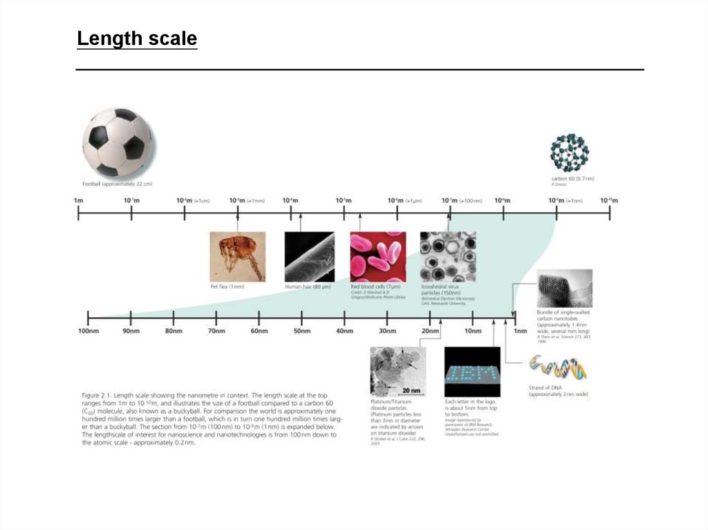
Length scale3. Fundamental Length Scales in Physics
QuantumQuantum Well:
Quantum Well Laser
Electric
Capacitor:
Single Electron Transistor
Magnetic
Magnetic Particle:
Data Storage Media
E1
E0
d
a = V1/3
Energy Levels
Charging Energy
Spin Flip Barrier
3h2/8m l2
2e2/ d
½ M2a3
l
l ~ 7 nm
d ~ 9 nm
a ~3 nm
4.
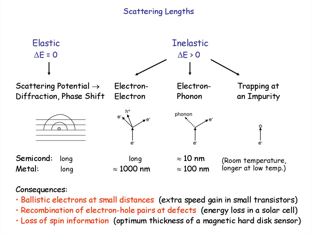
Scattering LengthsElastic
E = 0
Scattering Potential
Diffraction, Phase Shift
Inelastic
E > 0
ElectronElectron
h+
Trapping at
an Impurity
phonon
e-
e-
e-
Semicond: long
Metal:
long
ElectronPhonon
long
1000 nm
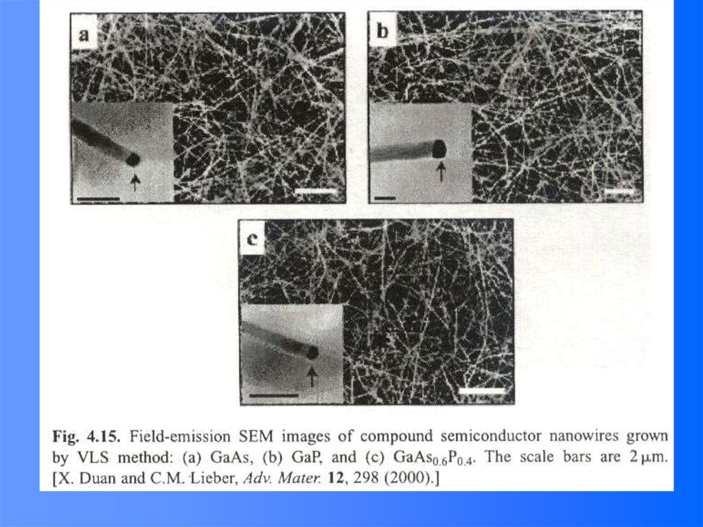
e-
e-
10 nm
100 nm
e-
(Room temperature,
longer at low temp.)
Consequences:
• Ballistic electrons at small distances (extra speed gain in small transistors)
• Recombination of electron-hole pairs at defects (energy loss in a solar cell)
• Loss of spin information (optimum thickness of a magnetic hard disk sensor)
5.
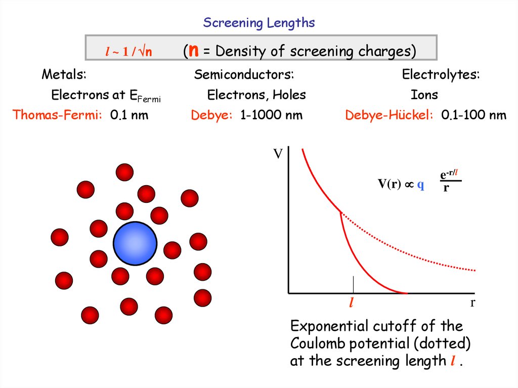
Screening Lengthsl ~ 1 / n
Metals:
Electrons at EFermi
Thomas-Fermi: 0.1 nm
(n = Density of screening charges)
Semiconductors:
Electrolytes:
Electrons, Holes
Debye: 1-1000 nm
Ions
Debye-Hückel: 0.1-100 nm
V
V(r) q
l
e-r/l
r
r
Exponential cutoff of the
Coulomb potential (dotted)
at the screening length l .
6. Length Scales in Polymers (including Biopolymers, such as DNA and Proteins)
Random Walk, EntropyStiffness vs. kBT
Radius of Gyration
(overall size, N straight segments)
Persistence Length
(straight segment)
lP
RG
RG lP N
cos = 1/e
a
lP = / kBT
Copolymers
DNA (double)
Polystyrene
RG 20-50 nm
lP 50 nm
lP 1 nm
7.
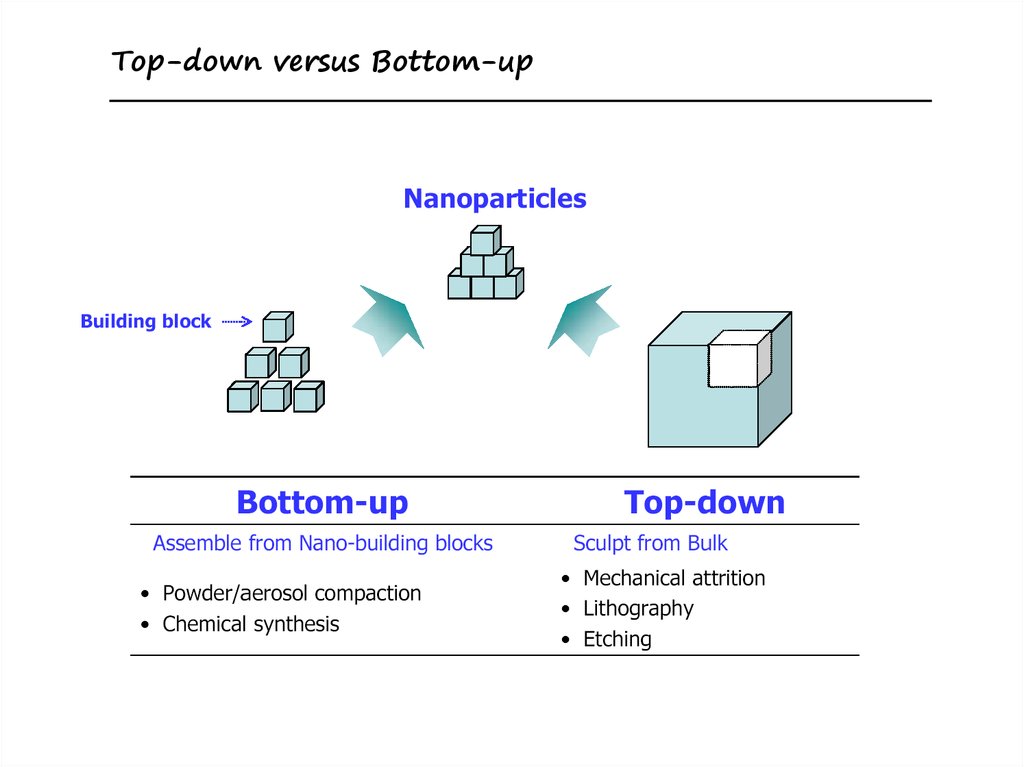
Top-down versus Bottom-up8. Nucleation and Growth of Crystals
9.
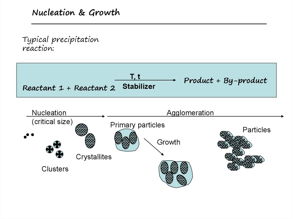
Nucleation & GrowthTypical precipitation
reaction:
T, t
Reactant 1 + Reactant 2 Stabilizer
Nucleation
(critical size)
Product + By-product
Agglomeration
Primary particles
Growth
Crystallites
Clusters
Particles
10. Nucleation and Growth Rates Control Rc
• Nucleation, the first step…• First process is for microscopic clusters
(nuclei) of atoms or ions to form
– Nuclei possess the beginnings of the structure of
the crystal
– Only limited diffusion is necessary
– Thermodynamic driving force for crystallization
must be present
11. Nucleation Rate – Thermodynamic barrier W*
W*+
0
-
r*
r
WS = 4 r2 ,
is the surface energy
WB = 4/3 r3 Gcrsyt(T),
the Gibb’s Free-Energy of
Crystallization
Wtot = WS + WB
• At r*, ( W(r)/ r)r=r* = 0
• r* = -2 / Gcryst(T)
• W(r*) W* = 16 3/3( Gcryst(T))2
12. Bottom-up Approaches
• Two approaches–thermodynamic equilibrium approach
• generation of supersaturation
• nucleation
• subsequent growth
–kinetic approach
• limiting the amount of precursors for the
growth
• confining in a limited space
13. Homogeneous nucleation
• Liquid, vapor or solid• supersaturation
–temperature reduction
–metal quantum dots in glass matrix by
annealing
–in situ chemical reactions (converting
highly soluble chemicals into less soluble
chemicals)
14. Homogeneous nucleation
• Driving forceGv
Fig 3.1
15. Homogeneous nucleation
• Energy barrier16
G
(3 Gv ) 2
*
r 2
*
Gv
Gibss free energy change
16. Nuclei
• formation favor:–high initial concentration or supersaturation
–low viscosity
–low critical energy barrier
• uniform nanoparticle size:
–same time formation
–abruptly high supersaturation -> quickly
brought below the minimum nucleation
concentration
17. Nuclei growth
• Steps–growth species generation
–diffusion from bulk to the growth surface
–adsorption
–surface growth
• size distribution
–A diffusion-limited growth VS. a
growth-limited processes
18. Ostwald ripening
• Many small crystals form in a systeminitially but slowly disappear except
for a few that grow larger, at the
expense of the small crystals. The
smaller crystals act as "nutrients" for
the bigger crystals. As the larger
crystals grow, the area around them
is depleted of smaller crystals.
19. “LEEM (Low-energy electron microscopy) images of ripening of single atomic layer height islands on Si(001) at various times
afterthe temperature was increased to 670˚ C: (a) 10 s, (b) 50 s, (c) 400
s, and (d) 1300 s.
20. Metallic nanoparticles
• Reduction of metal complexes indilute solution
–Diffusion-limited process maintaining
–Example: nano-gold particles
• chlorauric acid (2.5 x 10⁻⁴ M) 20 ml boiling
solution+ sodium citrate (0.5%) 1 ml
• 100°C till color change + water to maintain
volume
• uniform and stable 20 nm particles
21. Semiconductor nanoparticles
–Pyrolysis of organometallic precursor(s)dissolved in anhydrate solvents at elevated
temperatures in an airless environment in the
presence of polymer stabilizer (i.e., capping
material)
–Coordinating solvent
• Solvent + capping material
• phosphine + phosphine oxide (good candidate)
• controlling growth process, stabilizing the colloidal
dispersion, electronically passivating the surface
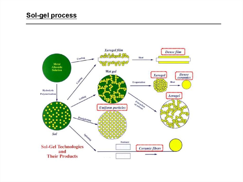
22. Oxide nanoparticles
• Several methods–principles: burst of homogeneous
nucleation + diffusion controlled growth
–most commonly: sol-gel processing
–most studied: silica colloids
23.
Sol-gel process24. SOL-GEL SCIENCE
Mix the reactives• Gelification
• Aging
Hydrolysis and
Condesation
• Soaking
Sol
Gelification
Gel
Aging
Drying
Gel
Aerogel
25. Gelification
ORMix reactives
OR
+
Si
OR
OR
H2O
OR
OR
OR
Si
OR
Hydrolysis and Condesation
OR
reactions take place
OR
+
OR
HO
OR
OR
+
HO
OR
OR
Gelification
Gel
OH
Aging
Gel
O
Si
OR
OR
Sol
Si
OR
OR
Si
OR
OR
OR
+
ROH
+
H2O
OR
Si
OR
OR
OR
OR
Si
ROH
OR
OR
Si
OR
+
Si
HO
O
Si
OR
OR
26. Sol-gel process
• Hydrolysis– e.g.
M (OEt ) 4 xH2O M (OEt ) 4 x (OH ) x xEtOH
• Condensation of precursors
– e.g.
M (OEt ) 4 x (OH ) x M (OEt ) 4 x (OH ) x
(OEt ) 4 x (OH ) x 1 MOM (OEt ) 4 x (OH ) x 1 H 2O
• typical precursors: metal alkoxides or
inorganic and organic salts
27. Sol-gel example: silica
• Precursors:–silicone alkoxides with different alkyl
ligand sizes
• catalyst:
Vigorous stirring
–ammonia
• solvent:
–various alcohols
water
28. Heterogeneous nucleation
• A new phase forms on a surface ofanother material
– thermal oxidation, sputtering and thermal
oxidation, Ar plasma and ulterior thermal
oxidation
– associate with surface defects (or edges)
29. Heterogeneous nucleation
30.
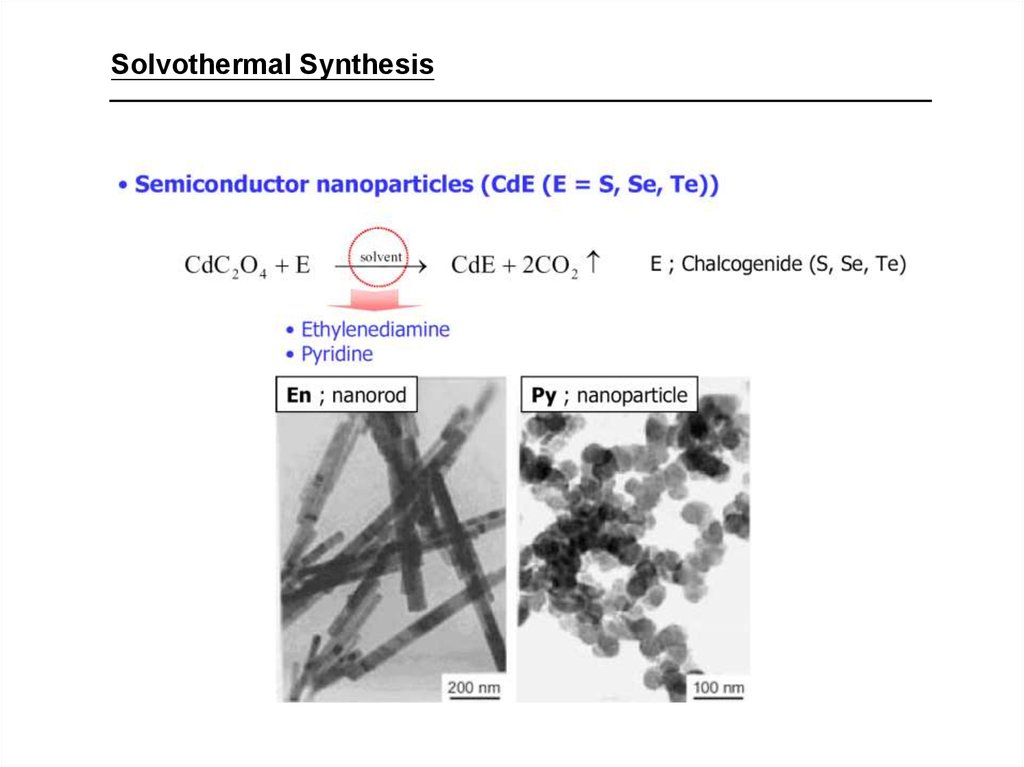
Solvothermal Synthesis31. Hydrothermal Synthesis
• The reactants are dissolved (orplaced) in water or another solvent
(solvothermal) in a closed vessel
• Bomb is heated above BP
• Conventional or MW oven
• Commercially:
–Tons of zeolites daily
32.
Solvothermal Synthesis33.
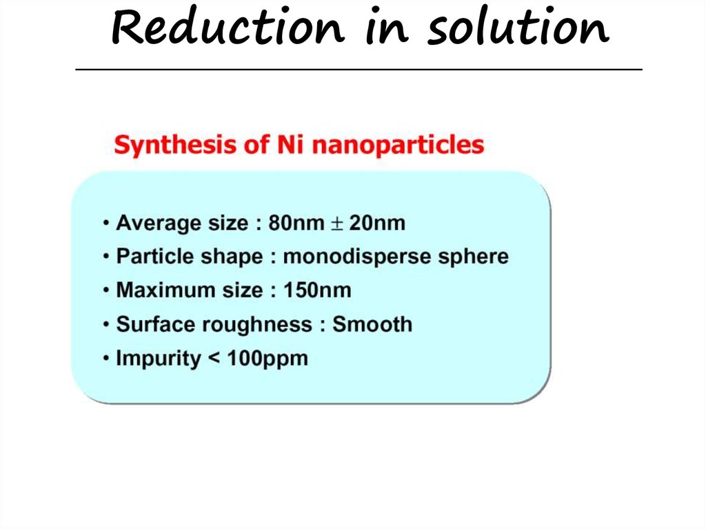
Reduction in solution34.
Reduction in solution35.
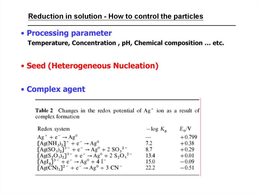
Reduction in solution - How to control the particles36.
Reduction in solution - How to control the particlesSeed-mediated growth
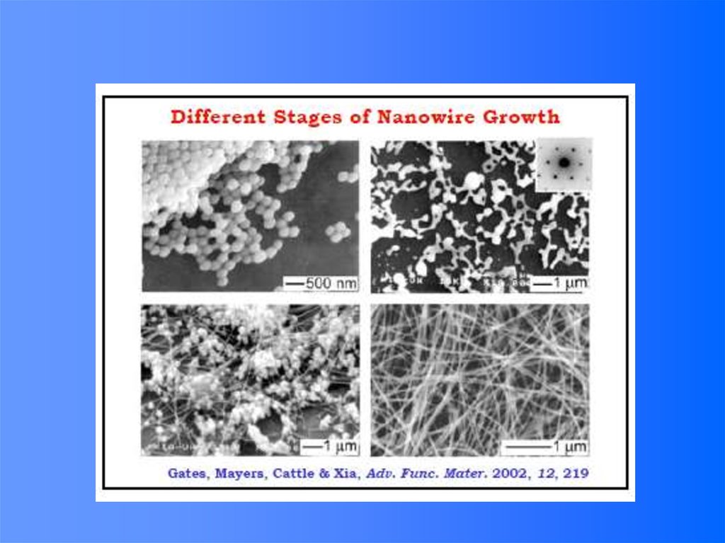
37. One dimensional nanostructures Nanowires Nanotubes
“They represent the smallest dimension forefficient transport of electrons and excitons,
and thus will be used as interconnects and
critical devices in nanoelectronics and nanooptoelectronics.”
General attributes & desired properties
Diameter – 10s of nanometers
Single crystal formation -- common
crystallographic orientation along the nanowire axis
Minimal defects within wire/tube
Minimal irregularities within nanowire/nanotube
38. Synthesis Methods
39. Spontaneous Growth
• A growth driven by reduction of Gibbsfree energy or chemical potential. This
can be from either recrystallization or
a decrease in supersaturation.
• Growth along a certain orientation
faster than other direction –
anisotropic growth.
• For nanowire/nanowire, growth occurs
only along one direction, but no
growth along other directions.
40. Growth of Single Crystal Nanobelts of Semiconducting or metal oxides
• Evaporating the metal oxides (ZnO, SnO2,In2O3, CdO) at high temperatures under a
vacuum of 300 torr and condensing on an
alumina substrate, placed inside the same
alumina tube furnace, at relatively low
temperature.
• Or heating the metal oxide or metal
nanoparticles at T=780 - 820oC in air,
Nanorods can be obtained depending upon
annealing T and time. Nanowires such as
ZnO, Ga2O3, MgO, CuO or Si3N4 and SiC
can be made by this method.
41.
42.
43.
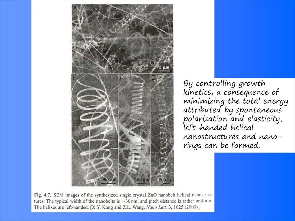
By controlling growthkinetics, a consequence of
minimizing the total energy
attributed by spontaneous
polarization and elasticity,
left-handed helical
nanostructures and nanorings can be formed.
44. Dissolution and Condensation Growth
• The growth species first dissolve intoa solvent or a solution, and then
diffuse through the solvent and
deposit onto the surface resulting
growth of nanowires.
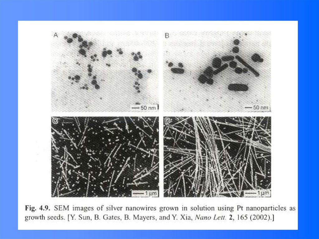
45. Growth of Ag Nanowire Using Pt Nanoparticles as Growth Seeds
• Precursor: AgNO3• Reduction agent: ethylene glycol
• Surfactant: polyvinyl pyrrolidone
(PVP)
• The surfactant absorbed on some
growth surfaces and blocks the
growth, resulting in the formation
of uniform crystalline silver
nanowires.
46.
47.
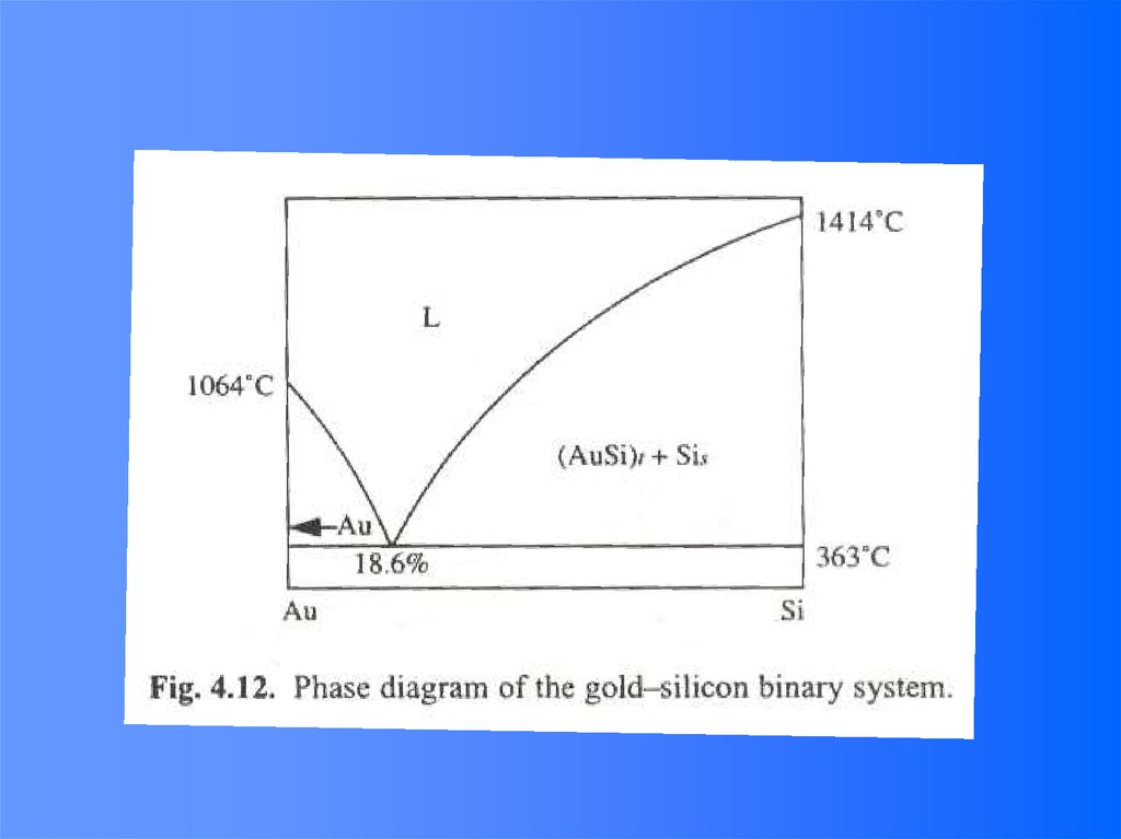
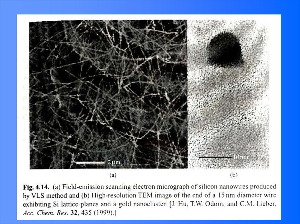
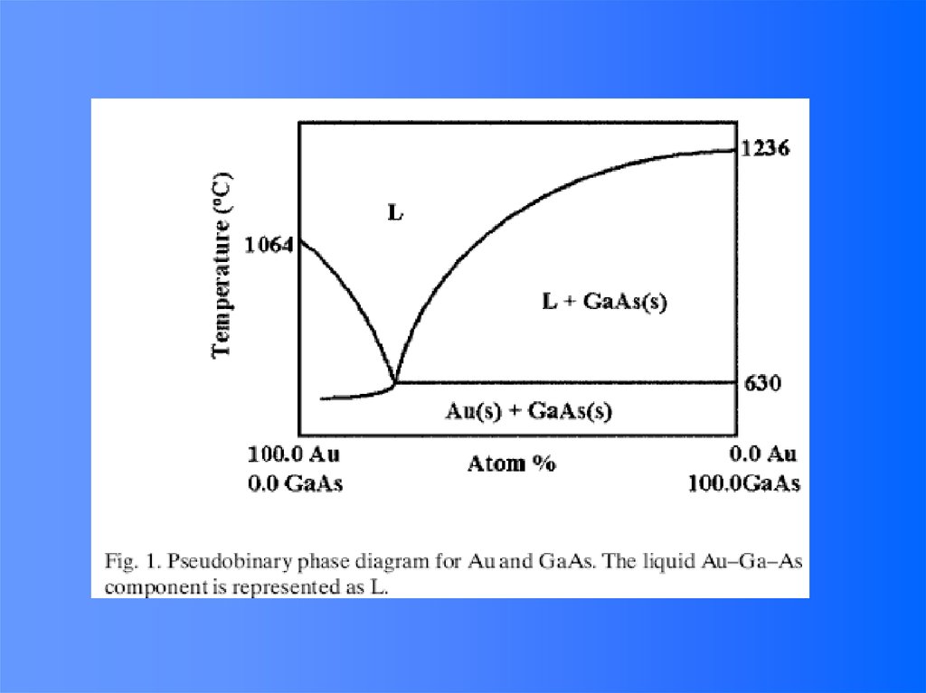
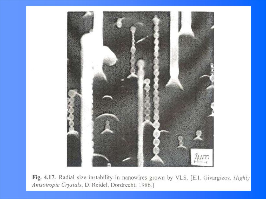
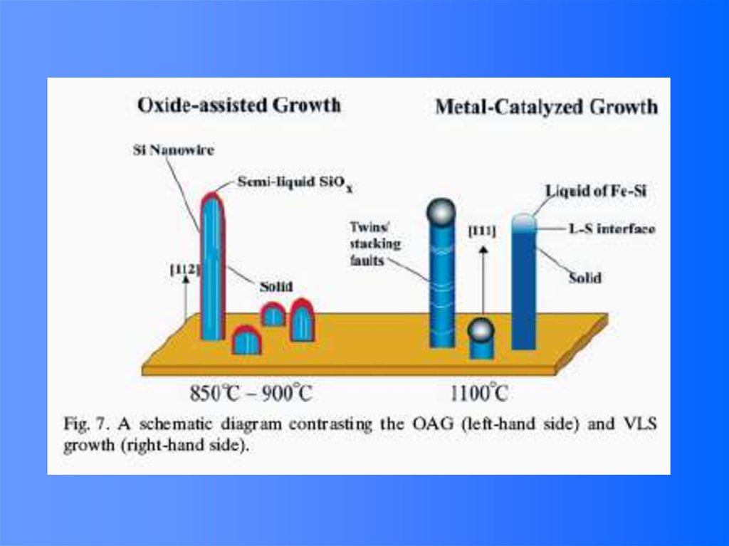
48. Vapor (or solution)-Liquid-solid (VLS) Growth
It is noted that the surface of liquid has a largeaccommodation coefficient, and is therefore a preferred site
for deposition.
49. VLS Growth Process
50.
51.
52. Compound Semiconductor Nanowires
• Nanowires of binary group III-Vmaterials (GaAs, GaP, InAs, and InP),
ternary
III-V materials (GaAs/P, InAs/P),
binary II-VI compounds (ZnS, ZnSe,
CdS, and CdSe), and binary IV-IV
SiGe alloys have been made in bulk
quantities as high purity (>90%) single
crystals.
53.
54. Table 1. Summary of single crystal nanowires synthesized. The growth temperatures correspond to ranges explored in these
studies. The minimum and average nanowire diameters were determined from TEM and FESEMimages. Structures were determined using electron diffraction and lattice resolved TEM imaging: ZB, zinc
blende; W, wurtzite; and D, diamond structure types. Compositions were determined from EDX measurements
made on individual nanowires. All of the nanowires were synthesized using Au as the catalyst, except GaAs, for
which Ag and Cu were also used. The GaAs nanowires obtained with Ag and Cu catalysts have the same size
distribution, structure, and composition as those obtained with the Au catalyst.
55.
56.
57.
58.
59.
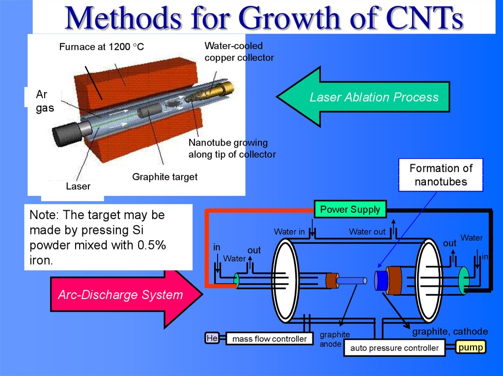
Methods for Growth of CNTsFurnace at 1200 C
Water-cooled
copper collector
Ar
gas
Laser Ablation Process
Nanotube growing
along tip of collector
Formation of
nanotubes
Graphite target
Laser
Note: The target may be
made by pressing Si
powder mixed with 0.5%
iron.
Power Supply
Water in
in
Water out
out
out
Water
in
Water
Arc-Discharge System
He
mass flow controller
graphite
anode
graphite, cathode
auto pressure controller
pump
60. CVD Growth of graphene
Hydrocarbon gas flowCarbon
dissolving
Metal
By-products
Boundary layer
Interface (negligible thickness)
Extremely fast
cooling
Fast/medium
cooling
Transport kinetics of gas species
Copper has zero solubility of carbon even at 1000oC
Carbon atoms form a graphene sheet directly during the growth step
Slow
cooling
61. Template assisted nanowire growth
Create a template for nanowires to growwithin
Based on aluminum’s unique property of
self organized pore arrays as a result of
anodization to form alumina (Al2O3)
Very high aspect ratios may be achieved
Pore diameter and pore packing densities
are a function of acid strength and voltage
in anodization step
Pore filling – nanowire formation via
various physical and chemical deposition
62. Al2O3 template preparation
Anodization of aluminumStart with uniform layer of ~1mm Al
Al serves as the anode, Pt may serve as the cathode,
and 0.3M oxalic acid is the electrolytic solution
Low temperature process (2-50C)
40V is applied
Anodization time is a function of sample size and
distance between anode and cathode
Key Attributes of the process (per M. Sander)
Pore ordering increases with template thickness – pores
are more ordered on bottom of template
Process always results in nearly uniform diameter pore,
but not always ordered pore arrangement
Aspect ratios are reduced when process is performed
when in contact with substrate (template is ~0.3-3
mm thick)
63.
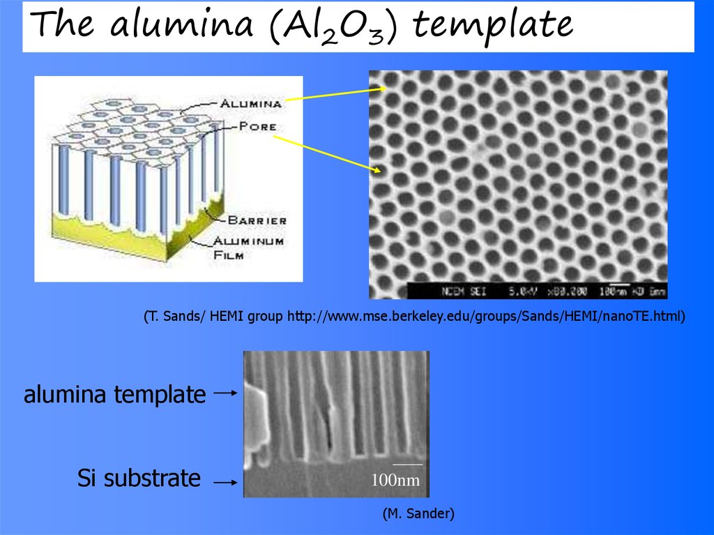
The alumina (Al2O3) template(T. Sands/ HEMI group http://www.mse.berkeley.edu/groups/Sands/HEMI/nanoTE.html)
alumina template
Si substrate
100nm
(M. Sander)
64. Electrochemical deposition
Works well with thermoelectric materials andmetals
Process allows to remove/dissolve oxide
barrier layer so that pores are in contact with
substrate
Filling rates of up to 90% have been achieved
Bi2Te3 nanowire
unfilled pore
alumina template
(T. Sands/ HEMI group http://www.mse.berkeley.edu/groups/Sands/HEMI/nanoTE.html)
65. Template-assisted, Au nucleated Si nanowires
Gold evaporated (Au nanodots) into thin ~200nmalumina template on silicon substrate
Ideally reaction with silane will yield desired
results
Need to identify equipment that will support this
process – contamination, temp and press issues
Additional concerns include Au thickness, Au on
alumina surface, template intact vs removed
Au dots
Au
100nm
1µm
(M. Sander)
template (top)