


 Etch")
 Etch")


")


 Английский язык
Похожие презентации:


Micro Fabrication Basics
1. Micro Fabrication Basics
2. Two Dominant Microsystems Fabrication Technologies
• SurfaceMicromachining
Robert Bosch GmbH
Sandia National Laboratories
IBM
• Bulk
Micromachining
HT Micro
3. Surface Micromachining
Based on CMOS manufacturing• Alternating structural and
sacrificial layers are deposited,
patterned and etched.
• Sacrificial layers are dissolved
away at the end to free the
structural layers so that they can
move.
• Materials are more or less restricted
to CMOS type materials (Poly
Crystalline silicon, Silicon oxide,
Silicon Nitride, BPSG, PSG)
4. Bulk Micromachining
• Consists of elements of surface micromachiningincluding deposition, patterning and etching of
structural and sacrificial layers.
• Also includes bulk dry or wet etching of relatively
large amounts of silicon substrate.
• Structures include high aspect ratio fluidic
channels, alignment grooves and the like coupled
with surface micromachined components included
thin membranes, thin piezoresistors, cantilevers…
5. Surface Micromachining Materials
• Sacrificial Layers– Silicon Dioxide
• Structural Layers
– Poly crystalline silicon (“Poly”)
• Insulators
– Silicon dioxide, Silicon Nitride
• Coatings
– SAM – Self Assembled Monolayer
6. Surface Micromachining Process Outline
Obtain Silicon Crystal Wafers
Deposit (or grow) thin film material
Pattern (Photo Lithography)
Etch (Wet and/or Dry Etch)
Deposit next film
Repeat Pattern, Etch, then Deposit again
Finally release structural layers by “dissolving”
the sacrificial layer away.
• Package and test parts
7. Cross Sectional View
8. Surface Micromachining Process
• Start with a Silicon CrystalSubstrate
• Slice and Polish to create wafers
Polish
Ingot
Slice Wafers
9. Grow Thermal Oxide
• First layer acts as aninsulator – it is a
thermally grown
silicon dioxide layer
Si + O2 -> SiO2
• Add heat to speed the
growth rate
• Add steam to speed it
up even further
Si + 2 H2O -> SiO2 + 2H2
10.
MEMS deposition technology can be classified in two groups:1. Depositions that happen because of a chemical reaction:
Chemical Vapor Deposition (CVD)
Electrodeposition
Epitaxy
Thermal oxidation
These processes exploit the creation of solid materials directly from chemical reactions
in gas and/or liquid compositions or with the substrate material. The solid material
is usually not the only product formed by the reaction. Byproducts can include
gases, liquids and even other solids.
2. Depositions that happen because of a physical reaction:
Physical Vapor Deposition (PVD)
Evaporation
Sputtering
Casting
Common for all these processes are that the material deposited is physically moved on
to the substrate. In other words, there is no chemical reaction which forms the material
on the substrate. This is not completely correct for casting processes, though it is
more convenient to think of them that way.
11. Thermal oxidation
Oxidation of the substrate surface in an oxygen rich atmosphere.The temperature is raised to 800° C-1100° C to speed up the
process. The growth of the film is spurned by diffusion of oxygen
into the substrate, which means the film growth is actually
downwards into the substrate. This process is naturally limited to
materials that can be oxidized, and it can only form films that are
oxides of that material. This is the classical process used to form
silicon dioxide on a silicon substrate.
12. Evaporation
In evaporation the substrate is placed inside a vacuum chamber, in which ablock (source) of the material to be deposited is also located. The source
material is then heated to the point where it starts to boil and evaporate. The
vacuum is required to allow the molecules to evaporate freely in the chamber,
and they subsequently condense on all surfaces
13. Sputtering
The substrate is placed in a vacuum chamber with the source material, named atarget, and an inert gas (such as argon) is introduced at low pressure. A gas plasma
is struck using an RF power source, causing the gas to become ionized. The ions are
accelerated towards the surface of the target, causing atoms of the source material to
break off from the target in vapor form and condense on all surfaces including the
substrate.
14. Casting
In this process the material to be deposited is dissolved in liquid form in a solvent.The material can be applied to the substrate by spraying or spinning. Once the
solvent is evaporated, a thin film of the material remains on the substrate.
This is particularly useful for polymer materials, which may be easily dissolved in
organic solvents, and it is the common method used to apply photoresist to
substrates (in photolithography).
15. Basic Idea behind lithographic processing
16. Basic Idea behind lithographic processing
17. Essential Lithography Steps
• Coat wafer withphoto resist
• Expose resist to a
pattern
• Develop resist
• Bake resist to
withstand
subsequent etch
process.
MATEC
18. Lithographic Processing: Wafers
19. Film growth/deposition
20. Photoresist Spinning
21. Masking and Exposure
22. Developing the Pattern
23. Etch the Material
24. Repeat Process
25. Final Release
26. Pattern Transfer
Lithography in the MEMS context is typically the transfer of a pattern to aphotosensitive material by selective exposure to a radiation source such as light.
A photosensitive material is a material that experiences a change in its physical
properties when exposed to a radiation source. If we selectively expose a
photosensitive material to radiation (e.g. by masking some of the radiation) the pattern
of the radiation on the material is transferred to the material exposed.
27. Resist
When resist is exposed to a radiation source of a specific a wavelength, thechemical resistance of the resist to developer solution changes.
If the resist is placed in a developer solution after selective exposure to a light
source, it will etch away one of the two regions (exposed or unexposed).
If the exposed material is etched away by the developer and the unexposed
region is resilient, the material is considered to be a positive resist.
If the exposed material is resilient to the developer and the unexposed region is
etched away, it is considered to be a negative resist.
28.
29. Positive and negative resist
30. Positive Resist Chemistry
31. Molecular weight shift
32. Typical Positive Resist process
EXAMPLE PROCESS: AZ5206 POSITIVE MASK PLATE• Soak mask plate in acetone > 10 min to remove the original photoresist.
Rinse in isopropanol, blow dry.
• Clean the plate with RIE in oxygen. Do not use a barrel etcher.
RIE conditions: 30 sccm O2, 30 mTorr total pressure, 90 W (0.25 W/cm2), 5
min.
• Immediately spin AZ5206, 3 krpm.
• Bake at 80 C for 30 min.
• Expose with e-beam, 10 kV, 6 C/cm2, Make sure the plate is well grounded.
(Other accelerating voltages may be used, but the dose will be different.)
• Develop for 60 s in KLK PPD 401 developer. Rinse in water.
• Descum - important Same as step 2 above, for only 5 seconds
Or use a barrel etcher, 0.6 Torr oxygen, 150W, 1 min.
• If this is a Cr plate, etch with Transene Cr etchant, ~1.5 min.
If this is a MoSi plate, then RIE etch:
0.05 Torr total pressure, 0.05 W/cm2, 16 sccm SF6, 4.2 sccm CF4,1 min.
• Plasma clean to remove resist: same as step 2 above, for 3 min.
33. Negative Resist Cemistry
34. Typical Negative resist process
EXAMPLE PROCESS: SAL NEGATIVE MASK PLATE•Soak mask plate in acetone > 10 min to remove photoresist.
•Clean the plate with RIE in oxygen. Do not use a barrel etcher.
RIE conditions: 30 sccm O2, 30 mTorr total pressure, 90 W (0.25 W/cm2), 5 min.
•Immediately spin SAL-601, 4 krpm, 1 min.
•Bake in 90 C oven for 10 min. This resist is not sensitive to room light.
•Expose at 50 kV, 11 C/cm2. Be sure the plate is grounded.
•Post-bake for 1 min on a large hotplate, 115 C.
•Cool for > 6 min.
•Develop for 6 min in Shipley MF312:water (1:1) Be sure to check for
underdevelopment.
•Descum 30 s with oxygen RIE: same as step 2, 10 s.
•Etch with Transene or Cyantek Cr etchant, ~1.5 min.
•Plasma clean to remove resist: Same as step 2, 5 min.
35.
Lithography is the principal mechanism for pattern definition in micromachining.A photosensitive layer is often used as a temporary mask when etching an underlying
layer, so that the pattern may be transferred to the underlying layer (shown in figure
3a). Photoresist may also be used as a template for patterning material deposited after
lithography (shown in figure 3b). The resist is subsequently etched away, and the
material deposited on the resist is "lifted off".
36. Alignment
In order to make useful devicesthe patterns for different
lithography steps that belong to a
single structure must be aligned
to one another.
The first pattern transferred to a
wafer usually includes a set of
alignment marks, which are high
precision features that are used
as the reference when positioning
subsequent patterns, to the first
pattern.
Each pattern layer should have an
alignment feature so that it may
be registered to the rest of the
layers.
37.
Depending on the lithography equipment used, the feature on the mask used forregistration of the mask may be transferred to the wafer. In this case, it may be
important to locate the alignment marks such that they don't affect subsequent wafer
processing or device performance.
Transfer of mask registration feature to substrate during lithography (contact aligner)
38.
The alignment mark shown below will cease to exist after a through the wafer DRIEetch. Pattern transfer of the mask alignment features to the wafer may obliterate the
alignment features on the wafer. In this case the alignment marks should be designed
to minimize this effect, or alternately there should be multiple copies of the alignment
marks on the wafer, so there will be alignment marks remaining for other masks to be
registered to.
Poor alignment mark design for a DRIE through the wafer etch (cross hair is released
and lost).
39. Exposure
At the edges of pattern light is scattered anddiffracted, so if an image is overexposed,
the dose received by photoresist at the edge
that shouldn't be exposed may become
significant.
If we are using positive photoresist, this will
result in the photoresist image being eroded
along the edges, resulting in a decrease in
feature size and a loss of sharpness or
corners.
If an image is severely underexposed, the
pattern may not be transferred at all, and
in less sever cases the results will be similar
to those for overexposure with the results
reversed.
40. The Lithography Module
Dehydration bake - dehydrate the wafer to aid resist adhesion.HMDS prime - coating of wafer surface with adhesion promoter. Not necessary for
all surfaces.
Resist spin/spray - coating of the wafer with resist either by spinning or spraying.
Typically desire a uniform coat.
Soft bake - drive off some of the solvent in the resist, may result in a significant
loss of mass of resist (and thickness). Makes resist more viscous.
Alignment - align pattern on mask to features on wafers.
Exposure - projection of mask image on resist to cause selective chemical
property change.
Post exposure bake - baking of resist to drive off further solvent content. Makes
resist more resistant to etchants (other than developer).
Develop - selective removal of resist after exposure (exposed resist if resist is
positive, unexposed resist if resist is positive). Usually a wet process (although dry
processes exist).
Hard bake - drive off most of the remaining solvent from the resist.
Descum - removal of thin layer of resist scum that may occlude open regions in
pattern, helps to open up corners.
41. Etching
In order to form a functional MEMS structure on a substrate, it is necessary toetch the thin films previously deposited and/or the substrate itself. In general,
there are two classes of etching processes:
Wet etching where the material is dissolved when immersed in a chemical
solution.
Dry etching where the material is sputtered or dissolved using reactive ions or a
vapor phase etchant.
42. Wet etching
Requires is a container with a liquid solution that will dissolve the material inquestion. Some single crystal materials, such as silicon, exhibit anisotropic
etching in certain chemicals.
Anisotropic etching in contrast to isotropic etching means different etch rates in
different directions in the material. The classic example of this is the <111> crystal
plane sidewalls that appear when etching a hole in a <100> silicon wafer in a
chemical such as potassium hydroxide (KOH). The result is a pyramid shaped
hole instead of a hole with rounded sidewalls with a isotropic etchant.
43. Dry Etching
The dry etching technology can split in three separate classes called reactive ionetching (RIE), sputter etching, and vapor phase etching.
In RIE, the substrate is placed inside a reactor in which several gases are
introduced. A plasma is struck in the gas mixture using an RF power source,
breaking the gas molecules into ions. The ions are accelerated towards, and reacts
at, the surface of the material being etched, forming another gaseous material. If the
ions have high enough energy, they can knock atoms out of the material to be
etched without a chemical reaction.
44. Anisotropic vs Isotropic Etch
45. Wet (Isotropic) Etch
46. Dry (Anisotropic) Etch
47. When do I want to use dry etching?
Sputter etching is essentially RIE without reactive ions. The systems used arevery similar in principle to sputtering deposition systems. The big difference is that
substrate is now subjected to the ion bombardment instead of the material target
used in sputter deposition.
Vapor phase etching is another dry etching method, which can be done with
simpler equipment than what RIE requires. In this process the wafer to be etched
is placed inside a chamber, in which one or more gases are introduced. The
material to be etched is dissolved at the surface in a chemical reaction with the
gas molecules.
The first thing you should note about this technology is that it is expensive to run
compared to wet etching. If you are concerned with feature resolution in thin film
structures or you need vertical sidewalls for deep etchings in the substrate, you
have to consider dry etching. If you are concerned about the price of your process
and device, you may want to minimize the use of dry etching. The IC industry has
long since adopted dry etching to achieve small features, but in many cases
feature size is not as critical in MEMS.
48. Wafer Example
Design Masks
Silicon Substrate
Deposit 5K Oxide
Pattern Mask 1
Wet Etch (Timed BOE)
Strip Resist
Deposit Aluminum (PVD Evaporation)
Pattern Mask 2
Metal Etch
Clean Resist
49. The Masks (Design)
Mask 1Mask 2
50. Bare Silicon
Start with Bare Crystalline Silicon51. Deposit Oxide
Thermally grow 5K Angstroms of Oxide52. Lithography – Resist Coat
Coat Oxide deposited wafer with Photo ResistPhoto resist is sensitive
to light – what is exposed
to UV becomes soluble
(what is clear on the
mask will get exposed
and subsequently
removed in the develop
step)
Mask which
will be used.
53. Exposure
Take the Coated WaferOverlay the first mask
Expose to UV Light
Remove Mask
Latent Image of Exposed Area
54. Develop
Take the exposedresist coated wafer.
And develop the
exposed resist.
The open area will
now be exposed to
the subsequent wet
etch step.
55. Wet Etch
Now you have an oxide coated wafer with a thinner opening.Take the patterned wafer
And place it in a BOE
(buffered oxide etch)
solution.
Time the etch carefully to
partially etch through the
oxide.
Remove the resist after etch
The orange color is due to a
different thickness of oxide.
56. Deposit Aluminum
Start with the etchedoxide wafer.
Deposit Aluminum
- PVD – Evaporation!
57. Mask 2 – Pattern & Etch Aluminum
Mask 2 – Pattern & Etch AluminumCoat Wafer with Resist
Overlay (place) Mask
Expose with UV Light
Develop away exposed
resist
Etch wafer.
Strip Resist
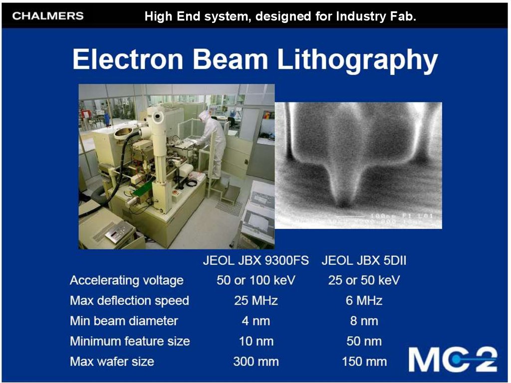
58. Electron Beam Lithography
59. Some things you can do with EBL
Circuit of SQUIDs and Josephson Tunnel Junctions60.
1.5 mmBonding
Pads
Contact “cage” to nano-circuit -- for rapid testing
61.
ConnectingStrips
62.
Ferromagnetic Normal metaltunnel junctions
100 nm
Co
Al
Circuit to measure spin injection from ferromagnet (Co) to normal metal (Al)
63.
Innerdigitated Capacitor incoplanar waveguide
Cooper Pair Transistor
64.
High End system, designed for Industry Fab.65. Micro Contact printing
66. Stamp fabrication
•Master made by direct writing methods (EBL on Si + etch)•Stamp gets dirty, wears out
•Essentially old-style printing methods scaled to nm dimensions