
 Промышленность
Похожие презентации:


")


Chemical Vapor Deposition (CVD)
1.
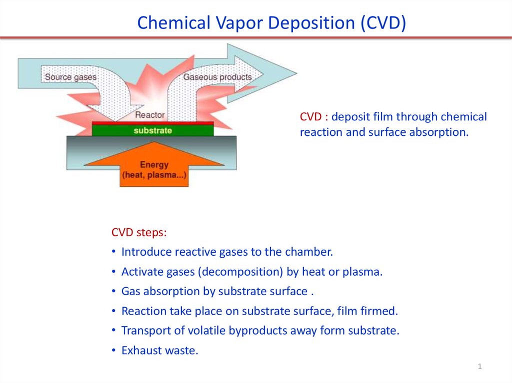
Chemical Vapor Deposition (CVD)CVD : deposit film through chemical
reaction and surface absorption.
CVD steps:
• Introduce reactive gases to the chamber.
• Activate gases (decomposition) by heat or plasma.
• Gas absorption by substrate surface .
• Reaction take place on substrate surface, film firmed.
• Transport of volatile byproducts away form substrate.
• Exhaust waste.
1
2.
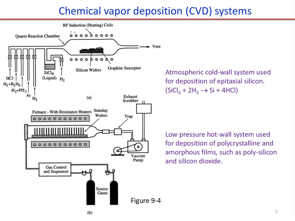
Chemical vapor deposition (CVD) systemsAtmospheric cold-wall system used
for deposition of epitaxial silicon.
(SiCl4 + 2H2 Si + 4HCl)
Low pressure hot-wall system used
for deposition of polycrystalline and
amorphous films, such as poly-silicon
and silicon dioxide.
Figure 9-4
2
3.
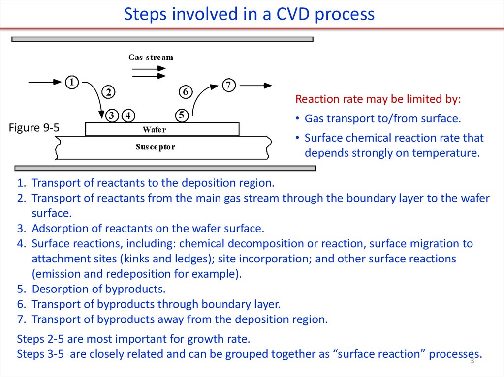
Steps involved in a CVD processGas stream
1
3
Figure 9-5
6
2
5
4
Wafer
Susceptor
7
Reaction rate may be limited by:
• Gas transport to/from surface.
• Surface chemical reaction rate that
depends strongly on temperature.
1. Transport of reactants to the deposition region.
2. Transport of reactants from the main gas stream through the boundary layer to the wafer
surface.
3. Adsorption of reactants on the wafer surface.
4. Surface reactions, including: chemical decomposition or reaction, surface migration to
attachment sites (kinks and ledges); site incorporation; and other surface reactions
(emission and redeposition for example).
5. Desorption of byproducts.
6. Transport of byproducts through boundary layer.
7. Transport of byproducts away from the deposition region.
Steps 2-5 are most important for growth rate.
Steps 3-5 are closely related and can be grouped together as “surface reaction” processes.
3
4.
Derivation of film growth rate(similar to/simpler than Deal-Grove model for thermal oxidation)
Boundary
layer
Gas
CG
F1
Figure 9-6
CS
F2
Silicon
F1 = diffusion flux of reactant species to the wafer through the
boundary layer (step 2) = mass transfer flux
(1)
F1 hG CG CS
where hG is the mass transfer coefficient (in cm/sec).
F2 = flux
of reactant consumed by the surface reaction (steps 35) = surface reaction flux,
(2)
F2 k S C S
where kS is the surface reaction rate (in cm/sec).
In steady state:
F = F1 = F2
(3)
k S 1
(4)
C S C G 1
Equating Equations (1) and (2) leads to
h G
k S hG CG
k S hG CT
F
v
Y (5)
The growth rate of the film is now given by
N k S hG N
k S hG N
where N is the number of atoms per unit volume
in the film and Y is the mole fraction (partial
pressure/total pressure) of the incorporating species, CT is total concentration of all molecules
4
in the gas phase .
5.
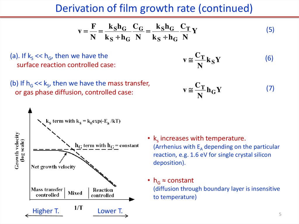
Derivation of film growth rate (continued)v
k h CG
k h CT
F
S G
S G
Y
N k S hG N k S hG N
(a). If kS << hG, then we have the
surface reaction controlled case:
(b) If hG << kS, then we have the mass transfer,
or gas phase diffusion, controlled case:
(5)
v
CT
k SY
N
(6)
v
CT
hGY
N
(7)
• ks increases with temperature.
(Arrhenius with EA depending on the particular
reaction, e.g. 1.6 eV for single crystal silicon
deposition).
• hG ≈ constant
(diffusion through boundary layer is insensitive
to temperature)
Higher T.
Lower T.
5
6.
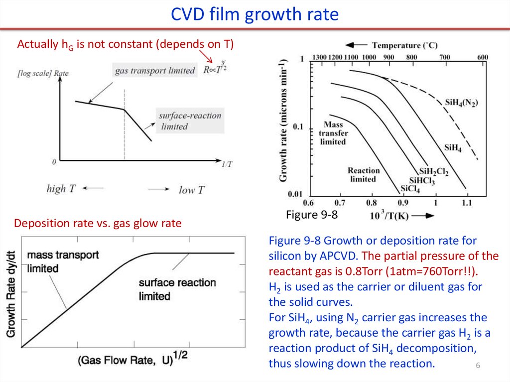
CVD film growth rateActually hG is not constant (depends on T)
Deposition rate vs. gas glow rate
Figure 9-8
Figure 9-8 Growth or deposition rate for
silicon by APCVD. The partial pressure of the
reactant gas is 0.8Torr (1atm=760Torr!!).
H2 is used as the carrier or diluent gas for
the solid curves.
For SiH4, using N2 carrier gas increases the
growth rate, because the carrier gas H2 is a
reaction product of SiH4 decomposition,
thus slowing down the reaction.
6
7.
Chemical Vapor Deposition (CVD) growth rate• kS limited deposition is VERY temperature sensitive.
E
k s k 0 exp a
kT
• hG limited deposition is VERY geometry (boundary layer) sensitive.
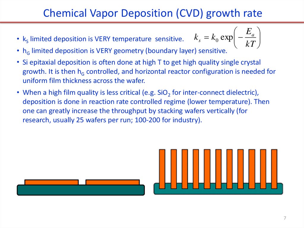
• Si epitaxial deposition is often done at high T to get high quality single crystal
growth. It is then hG controlled, and horizontal reactor configuration is needed for
uniform film thickness across the wafer.
• When a high film quality is less critical (e.g. SiO2 for inter-connect dielectric),
deposition is done in reaction rate controlled regime (lower temperature). Then
one can greatly increase the throughput by stacking wafers vertically (for
research, usually 25 wafers per run; 100-200 for industry).
7
8.
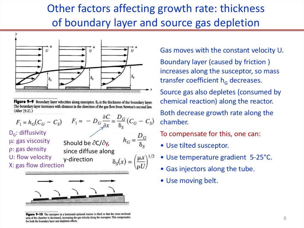
Other factors affecting growth rate: thicknessof boundary layer and source gas depletion
Gas moves with the constant velocity U.
Boundary layer (caused by friction )
increases along the susceptor, so mass
transfer coefficient hG decreases.
Source gas also depletes (consumed by
chemical reaction) along the reactor.
Both decrease growth rate along the
chamber.
DG: diffusivity
: gas viscosity
Should be C/ y,
: gas density
since diffuse along
U: flow velocity
y-direction
X: gas flow direction
To compensate for this, one can:
• Use tilted susceptor.
• Use temperature gradient 5-25°C.
• Gas injectors along the tube.
• Use moving belt.
8
9.
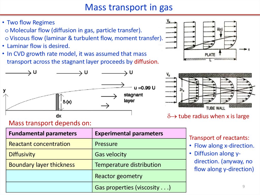
Mass transport in gas• Two flow Regimes
o Molecular flow (diffusion in gas, particle transfer).
o Viscous flow (laminar & turbulent flow, moment transfer).
• Laminar flow is desired.
• In CVD growth rate model, it was assumed that mass
transport across the stagnant layer proceeds by diffusion.
tube radius when x is large
Mass transport depends on:
Fundamental parameters
Experimental parameters
Reactant concentration
Pressure
Diffusivity
Gas velocity
Boundary layer thickness
Temperature distribution
Transport of reactants:
• Flow along x-direction.
• Diffusion along ydirection. (anyway, no
flow along y-direction)
Reactor geometry
Gas properties (viscosity . . .)
9
10.
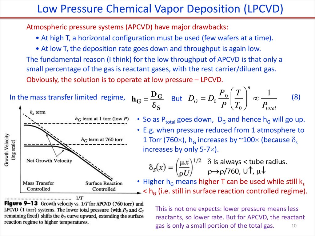
Low Pressure Chemical Vapor Deposition (LPCVD)Atmospheric pressure systems (APCVD) have major drawbacks:
• At high T, a horizontal configuration must be used (few wafers at a time).
• At low T, the deposition rate goes down and throughput is again low.
The fundamental reason (I think) for the low throughput of APCVD is that only a
small percentage of the gas is reactant gases, with the rest carrier/diluent gas.
Obviously, the solution is to operate at low pressure – LPCVD.
n
In the mass transfer limited regime, h G D G
S
But DG D0
P0 T
1
P T0
Ptotal
(8)
• So as Ptotal goes down, DG and hence hG will go up.
• E.g. when pressure reduced from 1 atmosphere to
1 Torr (760 ), hG increases by ~100 (because s
increases by only 5-7 ).
Is always < tube radius.
/760, U ,
• Higher hG means higher T can be used while still ks
< hG (i.e. still in surface reaction controlled regime).
This is not one expects: lower pressure means less
reactants, so lower rate. But for APCVD, the reactant
10
gas is only a small portion of the total gas.
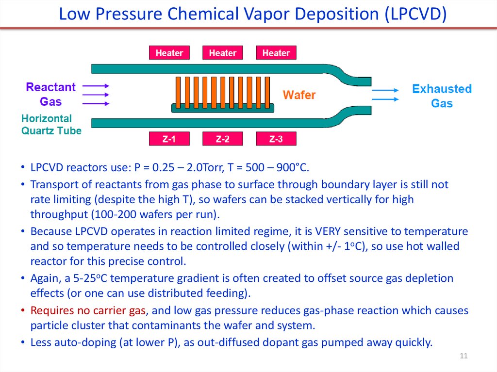
11.
Low Pressure Chemical Vapor Deposition (LPCVD)• LPCVD reactors use: P = 0.25 – 2.0Torr, T = 500 – 900°C.
• Transport of reactants from gas phase to surface through boundary layer is still not
rate limiting (despite the high T), so wafers can be stacked vertically for high
throughput (100-200 wafers per run).
• Because LPCVD operates in reaction limited regime, it is VERY sensitive to temperature
and so temperature needs to be controlled closely (within +/- 1oC), so use hot walled
reactor for this precise control.
• Again, a 5-25oC temperature gradient is often created to offset source gas depletion
effects (or one can use distributed feeding).
• Requires no carrier gas, and low gas pressure reduces gas-phase reaction which causes
particle cluster that contaminants the wafer and system.
• Less auto-doping (at lower P), as out-diffused dopant gas pumped away quickly.
11