


 Электроника
Похожие презентации:
. Junction field-effect transistor (JFET)")


")
")

")

Transistors
1.
Transistors.Presented by
Doctor PhD, assistant-professor
Asset Akhmadiya
2.
IntroductionThis lecture introduces the transistor. Transistors are solid-state
devices similar in some ways to the diodes you have studied. Transistors
are more complex and can be used in many more ways. The most
important feature of transistors is their ability to amplify signals and act as
switches. Amplification can make a weak signal strong enough to be
useful in an electronic application. For example, an audio amplifier can be
used to supply a strong signal to a loudspeaker.
3.
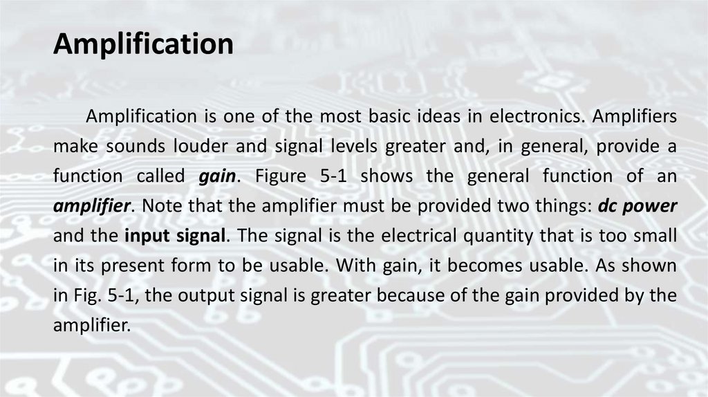
AmplificationAmplification is one of the most basic ideas in electronics. Amplifiers
make sounds louder and signal levels greater and, in general, provide a
function called gain. Figure 5-1 shows the general function of an
amplifier. Note that the amplifier must be provided two things: dc power
and the input signal. The signal is the electrical quantity that is too small
in its present form to be usable. With gain, it becomes usable. As shown
in Fig. 5-1, the output signal is greater because of the gain provided by the
amplifier.
4.
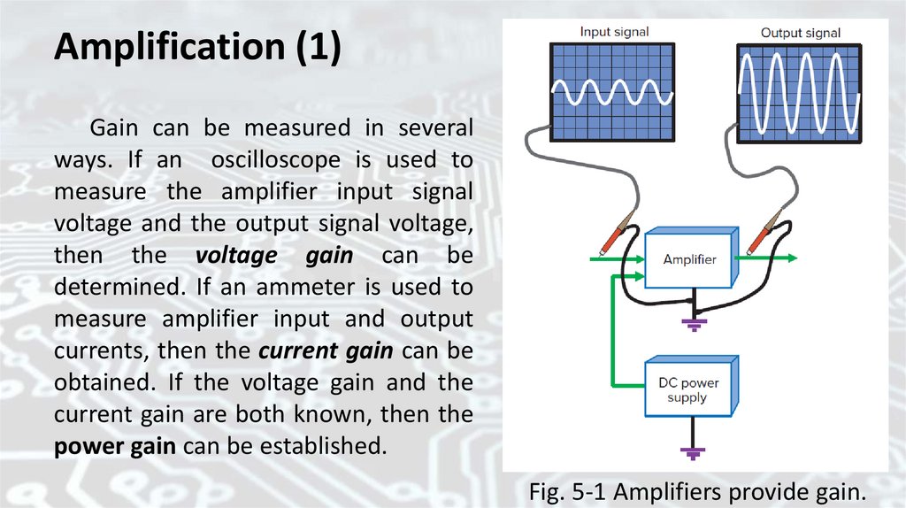
Amplification (1)Gain can be measured in several
ways. If an oscilloscope is used to
measure the amplifier input signal
voltage and the output signal voltage,
then the voltage gain can be
determined. If an ammeter is used to
measure amplifier input and output
currents, then the current gain can be
obtained. If the voltage gain and the
current gain are both known, then the
power gain can be established.
Fig. 5-1 Amplifiers provide gain.
5.
Calculation of the power gain6.
Power gainOnly amplifiers provide a power gain. Other devices might give a
voltage gain or a current gain, but not both. A step-up transformer
provides voltage gain but is not an amplifier. A transformer does not
provide any power gain. If the transformer steps up the voltage 10 times,
then it steps down the current 10 times. The power gain, ignoring loss in
the transformer, will be
A step-down transformer provides a current gain. It cannot be
considered an amplifier. The current gain is offset by a voltage loss,
and thus, there is no power gain.
7.
Amplification (2)Even though power gain seems to be the important idea, some
amplifiers are classified as voltage amplifiers. In some circuits, only the
voltage gain is mentioned. This is especially true in amplifiers designed to
handle small signals. You will run across many voltage amplifiers or smallsignal amplifiers in electronic systems. They provide power gain, too.
The term power amplifier is generally used to refer to amplifiers that
develop a large signal. In the electronic system in Fig. 5-2, the speaker
requires several watts for good volume. The signal from the Bluetooth
receiver is in the milliwatt (mW) region. A total power gain of hundreds is
needed. However, only the final large-signal amplifier is called a power
amplifier.
8.
Amplification (3)Fig. 5-2 Small-signal and large-signal
9.
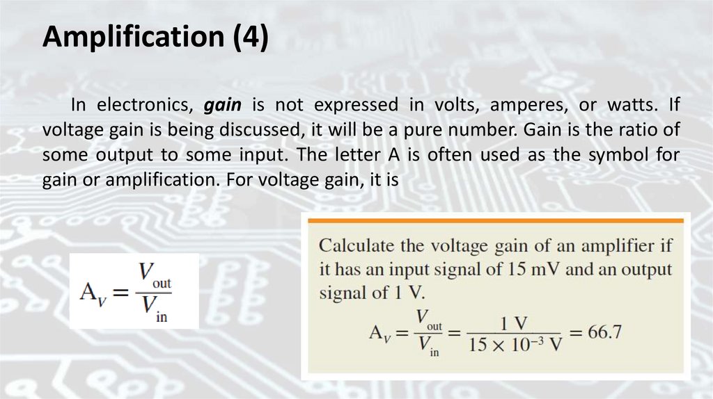
Amplification (4)In electronics, gain is not expressed in volts, amperes, or watts. If
voltage gain is being discussed, it will be a pure number. Gain is the ratio of
some output to some input. The letter A is often used as the symbol for
gain or amplification. For voltage gain, it is
10.
TransistorsTransistors provide the power gain that is needed for most electronic
applications. They also can provide voltage gain and current gain. There are
several important types of transistors. The most popular type is the bipolar
junction transistor (BJT). Field-effect transistors are also important. Both
types are covered here.
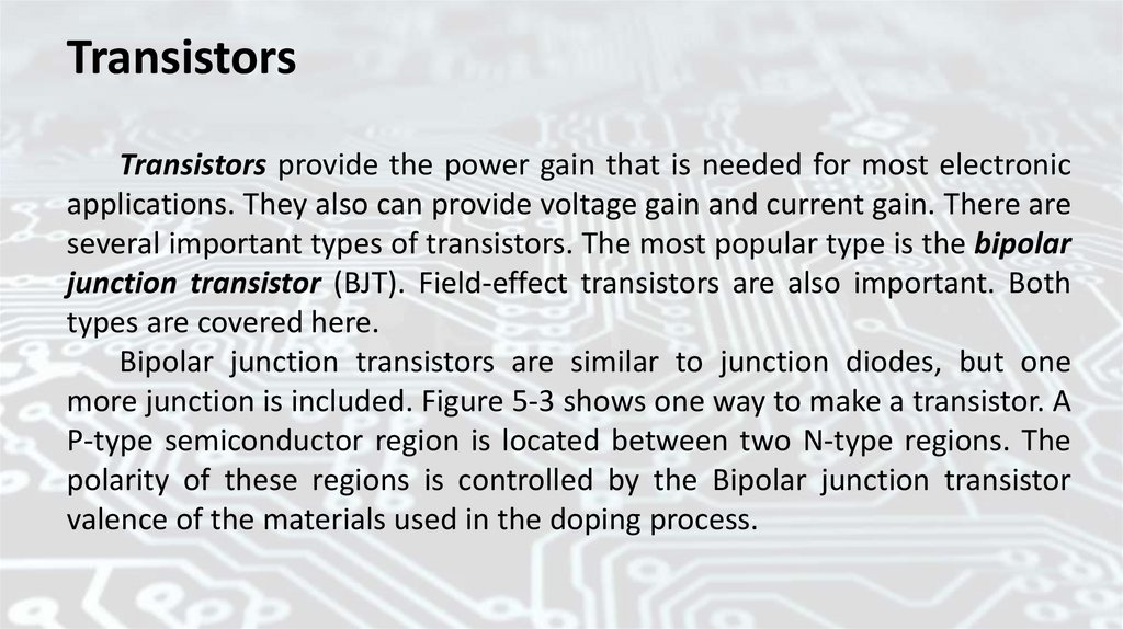
Bipolar junction transistors are similar to junction diodes, but one
more junction is included. Figure 5-3 shows one way to make a transistor. A
P-type semiconductor region is located between two N-type regions. The
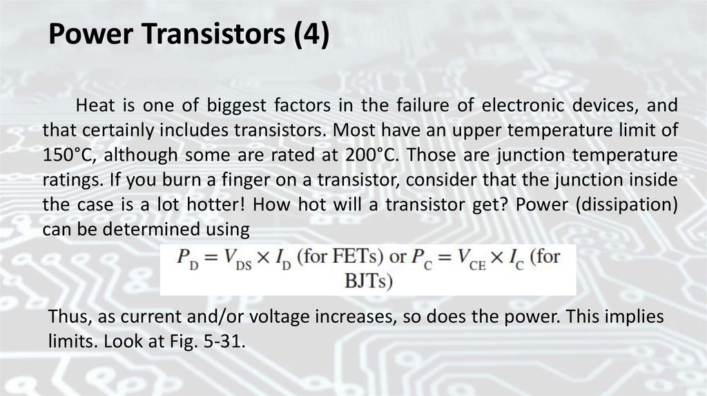
polarity of these regions is controlled by the Bipolar junction transistor
valence of the materials used in the doping process.
11.
Transistors (1)Fig. 5-3 NPN transistor structure.
12.
Transistors (2)The transistor regions shown in Fig. 5-3 are named emitter, collector,
and base. The emitter is very rich in current carriers. Its job is to send its
carriers into the base region and then on to the collector. The collector
collects the carriers. The emitter emits the carriers. The base acts as the
control region. The base can allow none, some, or many of the carriers to
flow from the emitter to the collector.
The transistor in Fig. 5-3 is bipolar because both holes (+) and
electrons (−) will take part in the current flow through the device. The Ntype regions contain free electrons, which are negative carriers. The Ptype region contains free holes, which are positive carriers. Two (bi)
polarities of carriers are present. Note that there are also two PN
junctions in the transistor. It is a BJT.
13.
Transistors (3)The transistor shown in Fig. 5-3 would be classified as an NPN
transistor. Another way to make a bipolar junction transistor is to make
the emitter and collector of P-type material and the base of N-type
material. This type would be classified as a PNP transistor. Figure 5-4
shows both possibilities and the schematic symbols for each. You should
memorize the symbols. Remember that the emitter lead is always the
one with the arrow. Also remember that if the arrow is Not Pointing iN,
the transistor is an NPN type.
14.
Transistors (4)The two transistor junctions must
be biased properly. This is why you
cannot replace an NPN transistor
with a PNP transistor. The polarities
would be wrong. Transistor bias is
shown in Fig. 5-5. The collector-base
junction must be reverse-biased for
proper operation. In an NPN
transistor, the collector will have to
be positive with respect to the base.
In a PNP transistor, the collector will
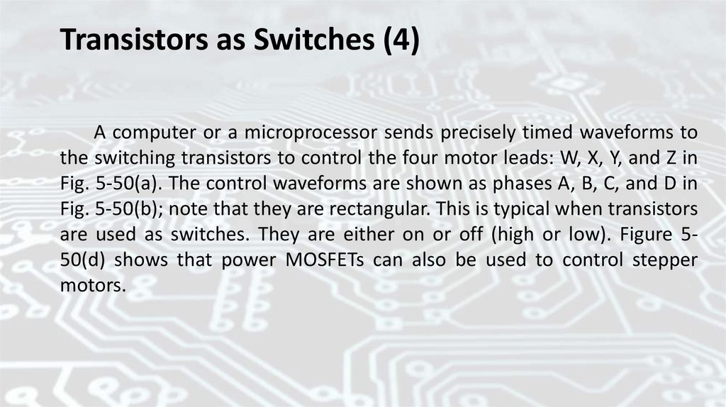
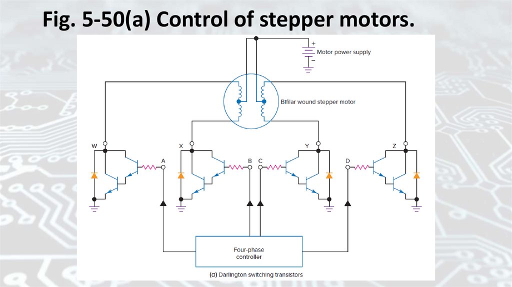
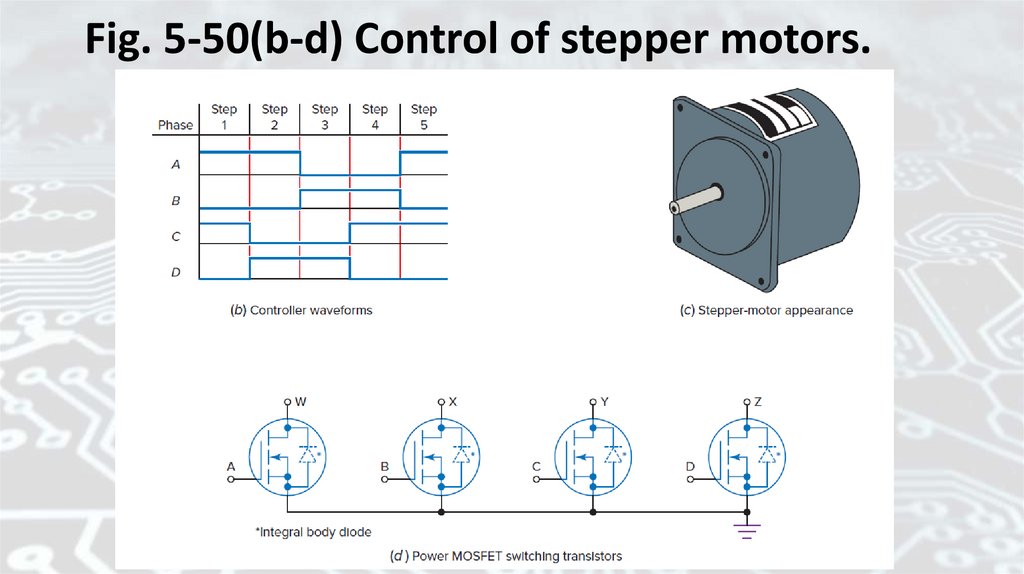
have to be negative with respect to
the base. PNP and NPN transistors
are not interchangeable.
Fig. 5-4 Transistor structures and symbols.
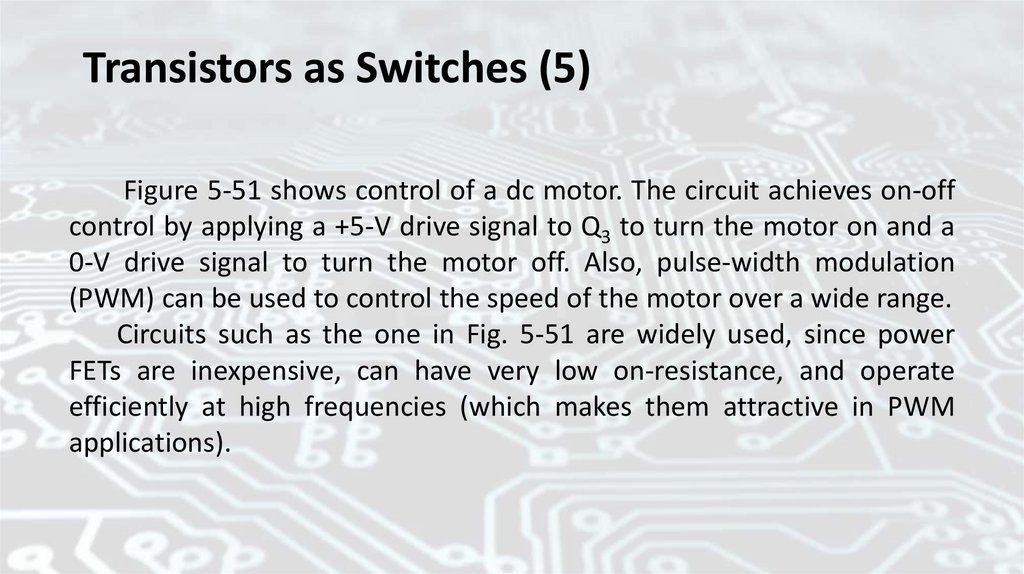
15.
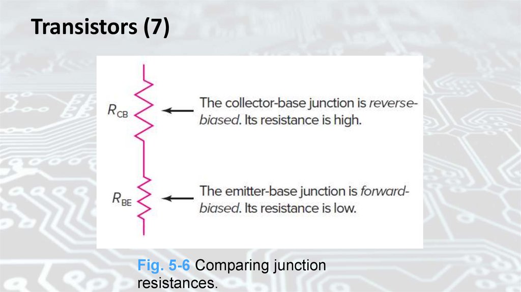
Transistors (5)The base-emitter junction
must be forward-biased to turn
the transistor on, as shown in Fig.
5-5. This makes the resistance of
the base-emitter junction very low
as compared with the resistance of
the collector-base junction. A
forward-biased
semiconductor
junction has low resistance. A
reverse-biased junction has high
resistance. Figure 5-6 compares
the two junction resistances.
Fig. 5-5 Biasing the transistor junctions.
16.
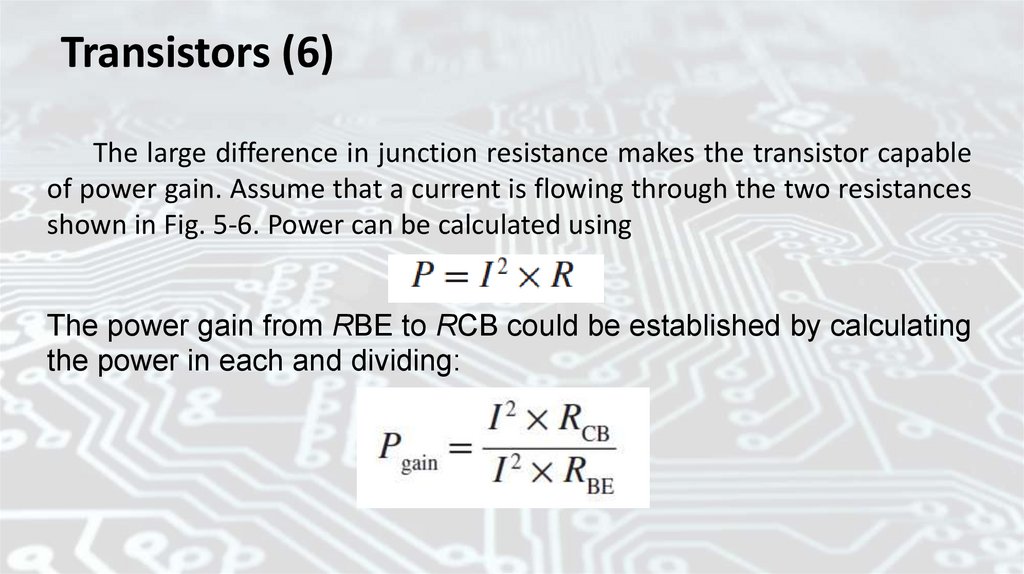
Transistors (6)The large difference in junction resistance makes the transistor capable
of power gain. Assume that a current is flowing through the two resistances
shown in Fig. 5-6. Power can be calculated using
The power gain from RBE to RCB could be established by calculating
the power in each and dividing:
17.
Transistors (7)Fig. 5-6 Comparing junction
resistances.
18.
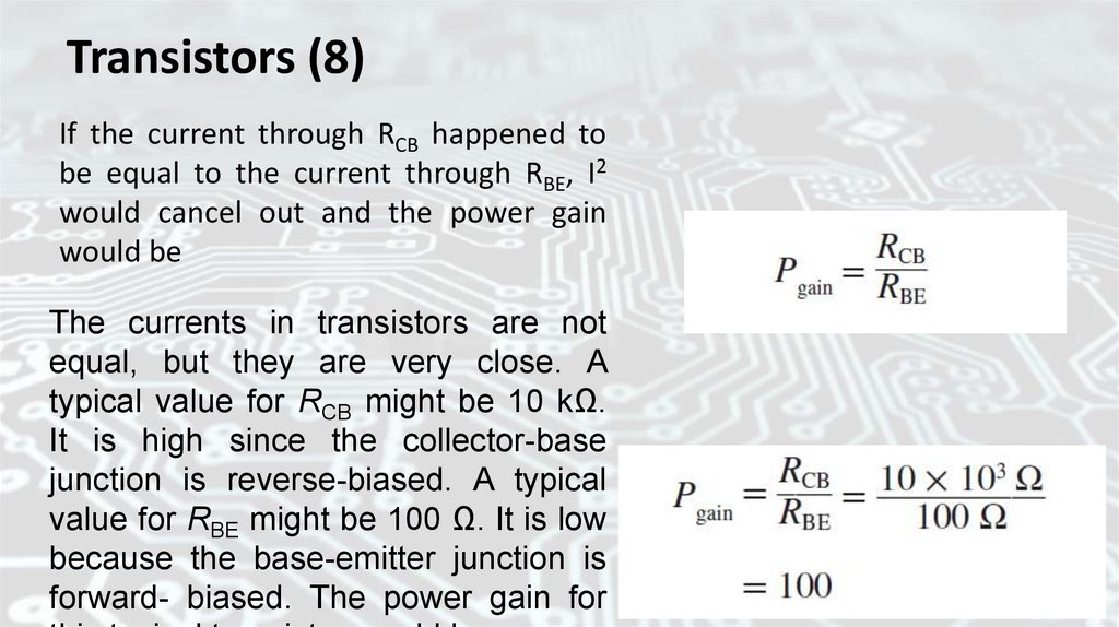
Transistors (8)If the current through RCB happened to
be equal to the current through RBE, I2
would cancel out and the power gain
would be
The currents in transistors are not
equal, but they are very close. A
typical value for RCB might be 10 kΩ.
It is high since the collector-base
junction is reverse-biased. A typical
value for RBE might be 100 Ω. It is low
because the base-emitter junction is
forward- biased. The power gain for
19.
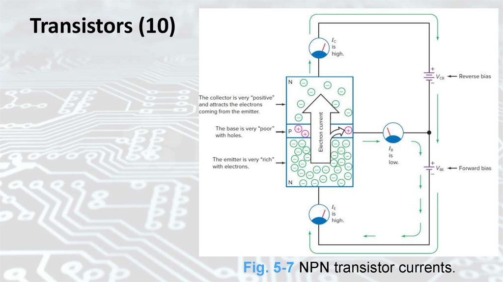
Transistors (9)Figure 5-7 shows why the collector-base junction current is high.
The collector-base voltage VCB produces a reverse bias across the
collector-base junction. The base-emitter voltage VBE produces a
forward bias across the base-emitter junction. If the transistor were
simply two diode junctions, the results would be as follows:
• IB and IE would be high.
• IC would be zero.
The base region of the transistor is very narrow (about 0.0025 cm, or
0.001 in.). The base region is lightly doped. It has only a few free holes. It is
not likely that an electron coming from the emitter will find a hole in the
base with which to combine.
20.
Transistors (10)Fig. 5-7 NPN transistor currents.
21.
Transistors (11)With so few electron-hole combinations in the base region, the base
current is very small. The collector is an N-type region but is charged
positively by VCB. Since the base is such a narrow region, the positive field
of the collector is quite strong, and the great majority of the electrons
coming from the emitter are attracted and collected by the collector. Thus,
• IE and IC are high.
• IB is low.
The emitter current in Fig. 5-7 is the highest current in the circuit. The
collector current is just a bit less. Typically, about 99 percent of the emitter
carriers go on to the collector. About 1 percent of the emitter carriers
combine with carriers in the base and become base current.
22.
Transistors (12)The current equation for Fig. 5-7 is
IE = I C + I B
By using typical percentages, it can be stated as
100% = 99% + 1%
The base current is quite small but very important. Suppose, for
example, that the base lead of the transistor in Fig. 5-7 is opened.
With the lead open, there can be no base current. The two voltages
VCB and VBE will add in series to make the collector positive with
respect to the emitter.
23.
Transistors (13)Current will continue to flow from the emitter to the collector, but it
does not. With no base current, there will be no emitter current and no
collector current. The base-emitter junction must be forward-biased for
the emitter to emit. Opening the base lead removes this forward bias. If
the emitter is not emitting, there is nothing for the collector to collect.
Even though the base current is very low, it must be present for the
transistor to conduct from emitter to collector.
The fact that a low base current controls much higher currents in the
emitter and collector is very important. This shows how the transistor is
capable of good current gain. Quite often, the current gain from the base
terminal to the collector terminal will be specified. This is one of the most
important transistor characteristics.
24.
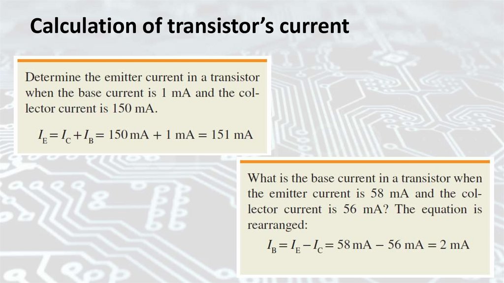
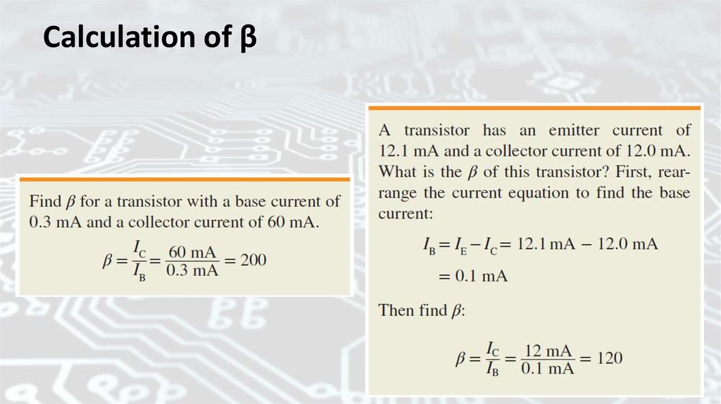
Calculation of transistor’s current25.
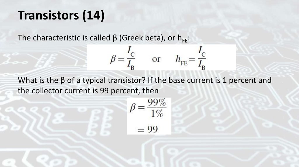
Transistors (14)The characteristic is called β (Greek beta), or hFE:
What is the β of a typical transistor? If the base current is 1 percent and
the collector current is 99 percent, then
26.
Calculation of β27.
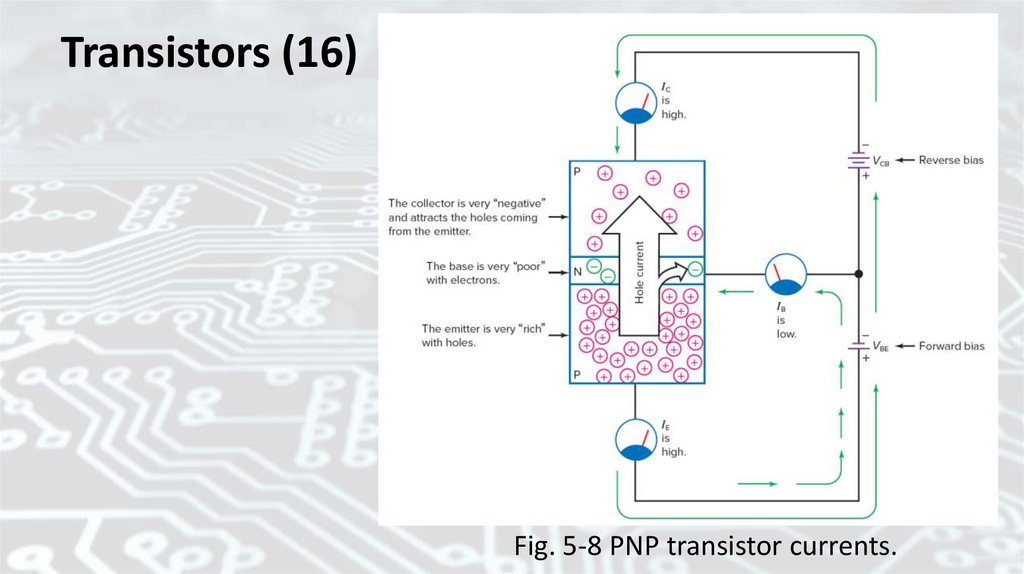
Transistors (15)Figure 5-8 shows the flow from emitter to collector as hole current. In
an NPN transistor, it is electron current. The two transistor structures
operate about the same in most ways. The emitter is very rich with
carriers. The base is quite narrow and has only a few carriers. The
collector is charged by the external bias source and attracts the carriers
coming from the emitter. The major difference between PNP and NPN
transistors is polarity.
The NPN transistor is more widely used than the PNP transistor.
Electrons have better mobility than holes; that is, they can move more
quickly through the crystal structure. This gives NPN transistors an
advantage in high-frequency circuits where things have to happen quickly.
28.
Transistors (16)Fig. 5-8 PNP transistor currents.
29.
Characteristic CurvesAs with diodes, transistor characteristic curves can provide much
information. There are many types of transistor characteristic curves. One
of the more popular types is the collector family of curves. An example of
this type is shown in Fig. 5-9. The vertical axis shows collector current (IC)
and is calibrated in milliamperes. The horizontal axis shows collectoremitter bias (VCE) and is calibrated in volts. Figure 5-9 is called a collector
family since several voltampere characteristic curves are presented for
the same transistor.
30.
Fig. 5-9 A collector family of curves for an NPNtransistor.
31.
Characteristic Curves (1)Figure 5-10 shows a circuit that can be used to measure the data
points for a collector family of curves. Three meters are used to monitor
base current IB, collector current IC, and collector-emitter voltage VCE. To
develop a graph of three values, one value can be held constant as the
other two vary. This produces one curve. Then the constant value is set to
a new level. Again, the other two values are changed and recorded. This
produces the second curve. The process can be repeated as many times
as required. For a collector family of curves, the constant value is the base
current.
32.
Fig. 5-10 Circuit for collecting transistor data.33.
Characteristic Curves (2)The variable resistor in Fig. 5-10 is adjusted to produce the desired
level of base current. Then the adjustable source is set to some value of
VCE. The collector current is recorded. Next, VCE is changed to a new
value. Again, IC is recorded. These data points are plotted on a graph to
produce a volt-ampere characteristic curve of IC versus VCE. A very
accurate curve can be produced by recording many data points. The next
curve in the family is produced in exactly the same way but at a new level
of base current.
The curves of Fig. 5-9 show some of the important characteristics of
junction transistors. Notice that over most of the graph, the collector
emitter voltage has little effect on the collector current.
34.
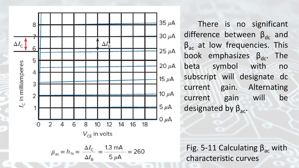
Characteristic Curves (3)The two prior calculations reveal another act about transistors. Not
only does β vary from transistor to transistor, but it also varies with IC.
Later, it will be shown that temperature also affects β.
What happens to a transistor when its base current is relatively
large? For example, what about Fig. 5-11 if IB = 1 mA? This is off the
graph! But it can be interpreted. First, this will not damage the transistor
unless its maximum collector dissipation rating is exceeded. This subject
will be covered a little later in this section. Transistors can be damaged by
excess base current, but something important happens before that
extreme is reached. The transistor will operate somewhere along the
steep vertical part of the characteristic curves.
35.
There is no significantdifference between βdc and
βac at low frequencies. This
book emphasizes βdc. The
beta symbol with no
subscript will designate dc
current gain. Alternating
current
gain
will
be
designated by βac.
Fig. 5-11 Calculating βac with
characteristic curves
36.
Transistors at high frequenciesAt high frequencies the ac current gain of BJTs starts to fall off. This
effect limits the useful frequency range of transistors. The gainbandwidth product is the frequency at which the ac current drain drops
to 1. The symbol for gain-bandwidth product is fT . This transistor
specification is important in high-frequency applications. For example,
the 2N5179 is a radio-frequency transistor and has an fT of 1.4 GHz.
The 2N3904 is a general-purpose transistor and has an fT of 300 MHz.
Thus, it would not be good practice to substitute a 2N3904 for a
2N5179 in a radiofrequency circuit.
37.
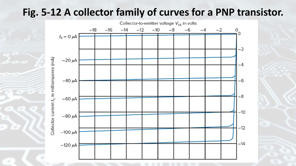
Characteristic Curves (4)It is standard practice to plot positive values to the right on the
horizontal axis and up on the vertical axis. Negative values go to the left
and down. A family of curves for a PNP transistor may be plotted on a
graph as shown in Fig. 5-12. The collector voltage must be negative in a
PNP transistor. Thus, the curves go to the left. The collector current is in
the opposite direction, compared with an NPN transistor. Thus, the curves
go down. However, curves for PNP transistors are sometimes drawn up and
to the right. Either method is equally useful for presenting the collector
characteristics.
Some shops and laboratories are equipped with a device called a curve
tracer. This device draws the characteristic curves on a cathode-ray tube or
liquid crystal display (LCD). This is far more convenient than collecting
many data points and plotting the curves by hand.
38.
Fig. 5-12 A collector family of curves for a PNP transistor.39.
Characteristic Curves (5)The transfer characteristic curves shown in Fig. 5-13 are another
example of how curves can be used to show the electrical characteristics
of a transistor. Curves of this type show how one transistor terminal (the
base) affects another (the collector). This is why they are called transfer
curves. Because that base current controls collector current. Figure 5-13
shows how base-emitter voltage controls collector current. This is because
the base-emitter bias sets the level of base current.
Figure 5-13 also shows one of the important differences between
silicon transistors and germanium transistors. Like diodes, germanium
transistors turn on at a much lower voltage ( approximately 0.2 V). The
silicon device turns on near 0.6 V. Germanium transistors are rarely used
now. They have been replaced by silicon devices because silicon works
better at high temperatures.
40.
Fig. 5-13 Comparing silicon and germaniumtransistors.
41.
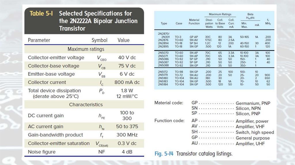
Transistor DataTransistor manufacturers prepare data sheets that detail the
mechanical, thermal, and electrical characteristics of the parts they
make. These data sheets are often bound into volumes called data
manuals. Table 5-1 is a sample from a data manual. It shows the
maximum ratings and some of the characteristics for 2N2222A
transistors. Data manuals also contain characteristic curves such as
those discussed previously.
Technicians usually try to replace a defective transistor with one
having the same part number. This is considered an “exact replacement”
even when the manufacturer is different. Sometimes it is impossible to
find an exact replacement. Data, such as those shown in Table 5-1, are
very useful in these cases.
42.
Transistor Data (1)Comparing two transistors often shows that they are very similar. For
example, the specifications of a 2N3904 transistor are strikingly similar to
those for a 2N2222A transistor shown in Table 5-1. One difference, not
shown in the table, is rise time, which is 25 ns for the 2N2222 and 35 ns
for the 2N3904. The 2N2222 is a switching transistor, so it is faster.
However, it is possible to substitute one device for the other in most
applications.
One way for a technician to learn something about a particular
transistor is to use substitution guides. These guides are not totally
accurate, but they do provide a good, general idea about the device of
interest. Another good source of information is a parts catalog. Figure
5-14 is a sample of transistor listings from a parts catalog.
43.
44.
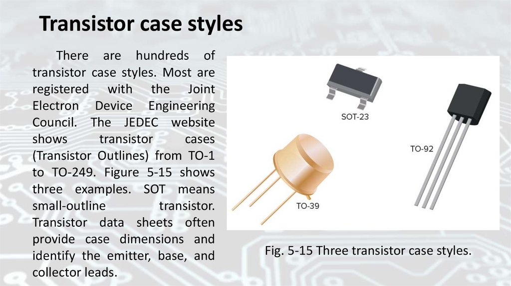
Transistor case stylesThere are hundreds of
transistor case styles. Most are
registered with the Joint
Electron Device Engineering
Council. The JEDEC website
shows
transistor
cases
(Transistor Outlines) from TO-1
to TO-249. Figure 5-15 shows
three examples. SOT means
small-outline
transistor.
Transistor data sheets often
provide case dimensions and
identify the emitter, base, and
collector leads.
Fig. 5-15 Three transistor case styles.
45.
Transistor replacementIn some cases the part number cannot be found in any of the
available guides or on the original transistor. It may be possible to use a
general type of unit in these situations. For example, the 2N2222A (or
the 2N3904) is a good, general-purpose replacement for small-signal
silicon NPN BJTs. Likewise, the 2N2905A (or the 2N3906) is a generalpurpose PNP replacement. General-purpose replacements should be
avoided in these cases:
• VHF or UHF applications
• High-power applications
• High-voltage applications
Substitute transistors must be of the same material and the same
polarity. Also, be sure that size and lead arrangements are compatible.
They must be based on the same technology.
46.
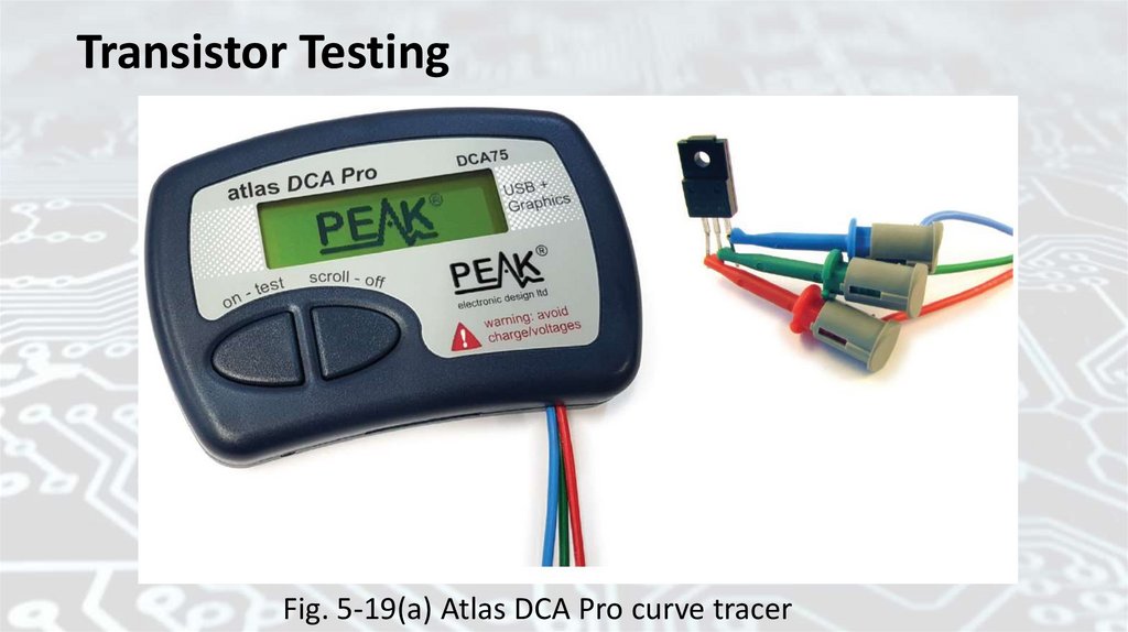
Transistor TestingOne way to test transistors is to use a curve tracer. This technique is
used by semiconductor manufacturers and by equipment makers to test
incoming parts. Curve tracers are also used in design labs. Figure 5-19 at
the end of this section shows an affordable curve tracer.
Another technique used at manufacturing and design centers is to
place the transistor in a special fixture or test circuit. This is a dynamic
test because it makes the device operate with real voltages and signals.
This method of testing is often used for VHF and UHF transistors.
Dynamic testing reveals power gain and noise figure under signal
conditions. Noise figure is a measure of a transistor’s ability to amplify
weak signals. Some transistors generate enough electrical noise to
overpower a weak signal. These transistors are said to have a poor noise
figure.
47.
Transistor TestingFig. 5-19(a) Atlas DCA Pro curve tracer
48.
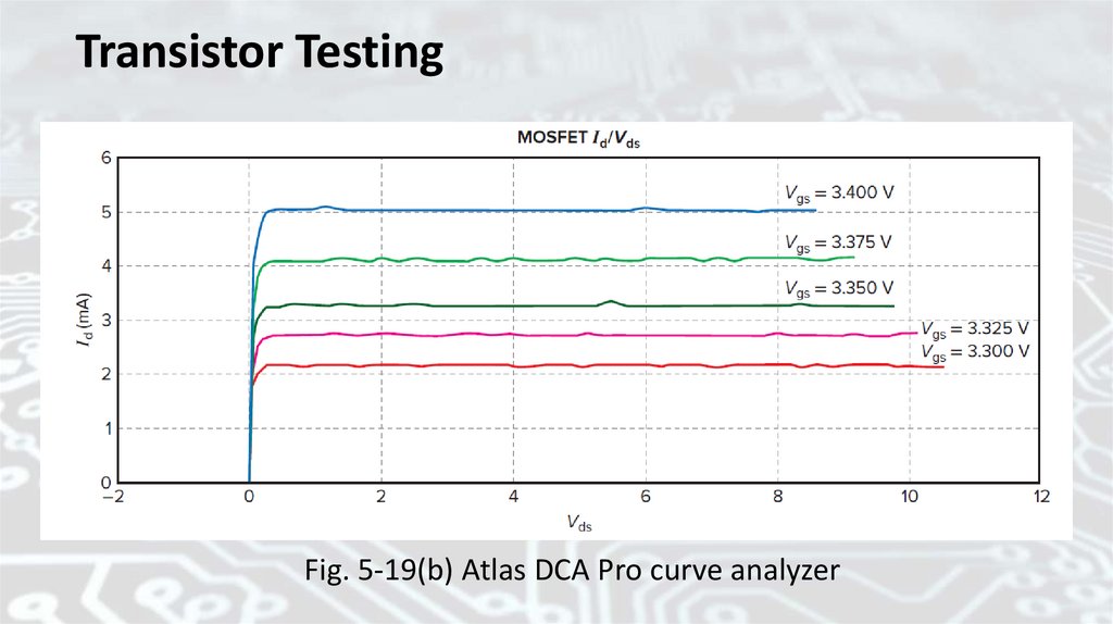
Transistor TestingFig. 5-19(b) Atlas DCA Pro curve analyzer
49.
Transistor Testing (1)A few transistor types may show a gradual loss of power gain. Radiofrequency power amplifiers, for example, may use overlay-type transistors.
These transistors can have over 100 separate emitters. They can suffer baseemitter changes that can gradually degrade power gain. Another problem is
moisture, which can enter the transistor package and gradually degrade
performance. Even though gradual failures are possible in transistors, they are
not typical.
For the most part, transistors fail suddenly and completely. One or both
junctions (the junction is the transition region between P and N) may shortcircuit. An internal connection can break loose or burn out from an overload.
This type of failure is easy to check. Most bad transistors can be identified
with a few ohmmeter tests out-of-circuit or with voltmeter checks in-circuit.
50.
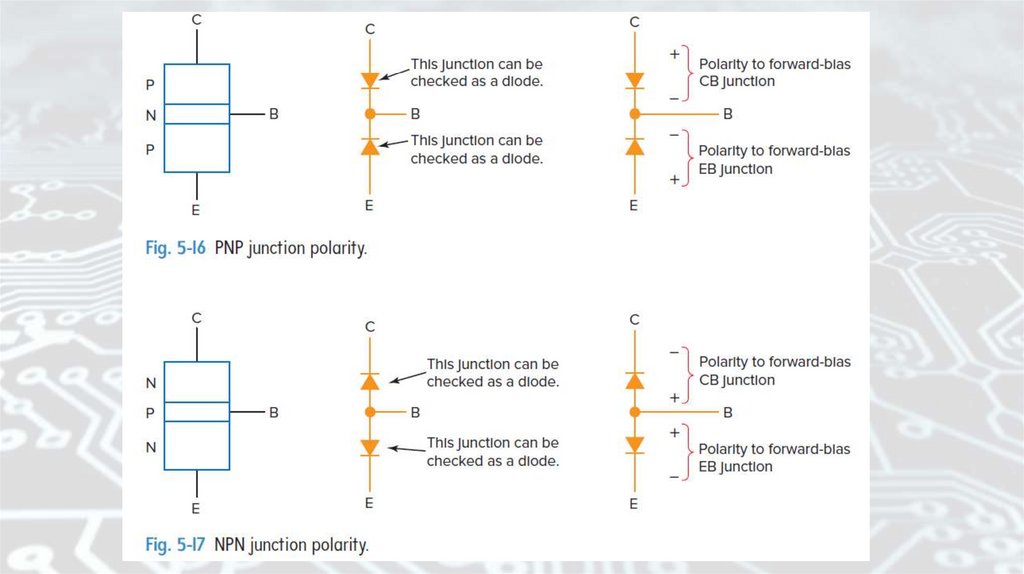
Transistor Testing (2)A good transistor has two PN junctions. Both can be checked with an
ohmmeter. As shown in Fig. 5-16, a PNP transistor is comparable to two
diodes with a common cathode connection. The base lead acts as the
common cathode. Figure 5-17 shows an NPN transistor as two diodes with
a common anode connection. If two good diodes can be verified by
ohmmeter tests, the transistor is probably good.
The ohmmeter can also be used to identify the polarity (NPN or PNP)
of a transistor and the three leads. This can be helpful when data are not
available. Analog ohmmeters should be set to the R × 100 range for testing
most transistors. For DMMs, the diode function can be used
51.
52.
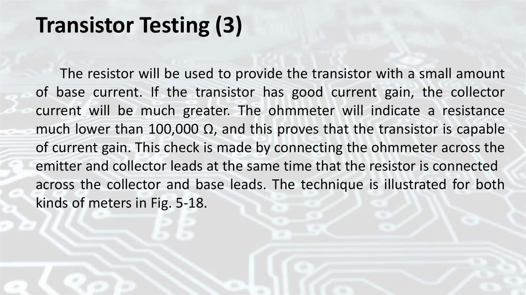
Transistor Testing (3)The resistor will be used to provide the transistor with a small amount
of base current. If the transistor has good current gain, the collector
current will be much greater. The ohmmeter will indicate a resistance
much lower than 100,000 Ω, and this proves that the transistor is capable
of current gain. This check is made by connecting the ohmmeter across the
emitter and collector leads at the same time that the resistor is connected
across the collector and base leads. The technique is illustrated for both
kinds of meters in Fig. 5-18.
53.
Transistor Testing (4)Fig. 5-18 Checking NPN gain.
54.
Transistor Testing (4)Transistors have some leakage current. This is due to minority carrier
action. One leakage current in a transistor is called ICBO. (The symbol I
stands for current, CB stands for the collector-base junction, and O tells us
the emitter is open.) This is the current that flows across the collector-base
junction under conditions of reverse bias and with the emitter lead open.
Another transistor leakage current is ICEO. (The symbol I stands for current,
CE stands for the collector-emitter terminals, and O tells us that the base
terminal is open.) ICEO is the largest leakage current. It is an amplified form
of ICBO:
55.
Transistor Testing (5)With the base terminal open, any current leaking across the reversebiased collector-base junction will have the same effect on the baseemitter junction as an externally applied base current. With the base
terminal open, there is no other place for the leakage current to go. The
transistor amplifies this leakage just as it would any base current:
Silicon transistors have very low leakage currents. When ohmmeter tests
are made, the ohmmeter should show an infinite resistance when the
junctions are reverse-biased. Anything less may mean the transistor is
defective. Germanium transistors have much greater leakage currents. This
will probably show up as a high, but not infinite, reverse resistance.
56.
Other Transistor TypesBipolar transistors use both holes and electrons as current carriers. A
unipolar (one-polarity) transistor uses only one type of current carrier. The
junction field-effect transistor (JFET) is an example of a unipolar transistor.
Figure 5-20 shows the structure and schematic symbol for an N-channel
JFET. Notice that the leads are named source, gate, and drain.
The JFET can be made in two ways. The channel can be N-type
material or P-type material. The schematic symbol in Fig. 5-20 is for an Nchannel device. The symbol for a P-channel device will show the arrow on
the gate lead pointing out. Remember, pointing iN indicates an N-channel
device. In a BJT, both holes and electrons are used to support conduction.
In an N-channel JFET, only electrons are used. In a P-channel JFET, only
holes are used.
57.
Other Transistor TypesFig. 5-20 An N-channel JFET.
58.
Other Transistor Types (1)The JFET operates in the depletion mode. A control voltage at the gate
terminal can deplete (remove) the carriers in the channel. For example, the
transistor in Fig. 5-20 will normally conduct from the source terminal to the
drain terminal. The N channel contains enough free electrons to support
the flow of current. If the gate is made negative, the free electrons can be
pushed out of the channel. Like charges repel. This leaves the channel with
fewer free carriers. The resistance of the channel is now much higher, and
this tends to decrease the source and drain currents. In fact, if the gate is
made negative enough, the device can be turned off and no current will
flow.
59.
Other Transistor Types (2)Examine the curves of Fig. 5-21. Notice that as the voltage from gate
to source (−VGS) increases, the drain current ID decreases. The curves in
Fig. 5-21 are sometimes divided into three regions: (1) the ohmic region
where the current ID increases rapidly from 0 to the bends, (2) the
saturation region where the curves are flat, and (3) the cutoff region
where the device is off and ID is 0. Compare a JFET with a BJT:
• A BJT is off (there is no collector current) until base current is provided.
• A JFET is on (drain current is flowing) until the gate voltage becomes
high enough to remove the carriers from the channel.
60.
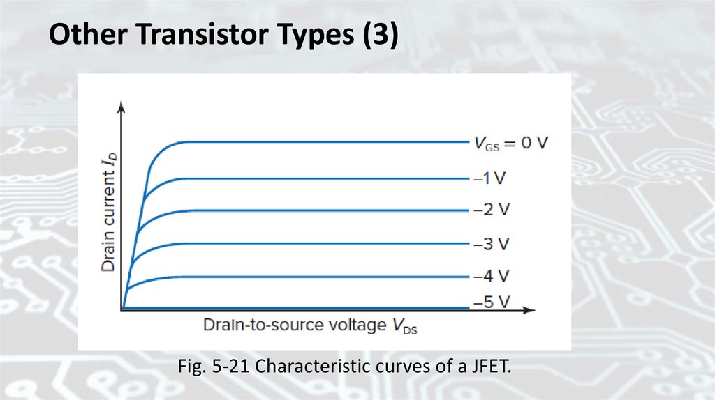
Other Transistor Types (3)Fig. 5-21 Characteristic curves of a JFET.
61.
Other Transistor Types (4)These are important differences: (1) The bipolar device is currentcontrolled. (2) The unipolar Device is voltage-controlled. (3) The bipolar
transistor is normally off. (4) The JFET is normally on.
Will there be any gate current in the JFET? Check Fig. 5-20. The gate
is made of P-type material. To control channel conduction, the gate is
made negative. This reverse-biases the gate channel diode. The gate
current should be zero (there may be a very small leakage current).
There are also P-channel JFETs. They use P-type material for the
channel and N-type material for the gate. The gate will be made positive
to repel the holes in the channel. Again, this reverse-biases the gatechannel diode, and the gate current will be zero if the gate voltage is high.
Since the polarities are opposite, N-channel JFETs and P-channel JFETs are
not interchangeable.
62.
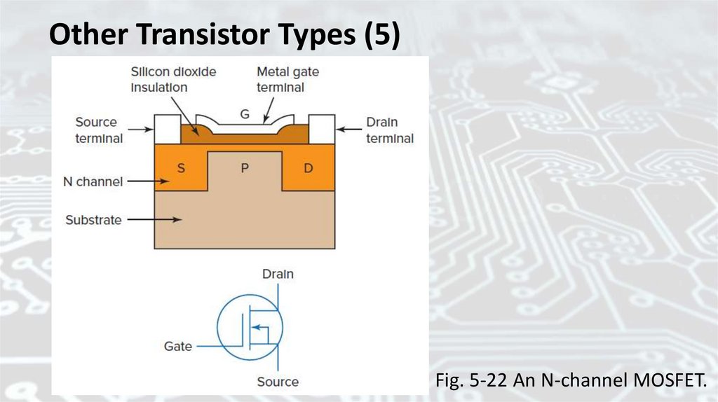
Other Transistor Types (5)Field-effect transistors (FETs) do not require any gate current for
operation. This means the gate structure can be completely insulated
from the channel. Thus, any slight leakage current resulting from minority
carrier action is blocked. The gate can be made of metal. The insulation
used is an oxide of silicon. This structure is shown in Fig. 5-22. It is called a
metal oxide semiconductor field-effect transistor (MOSFET). The MOSFET
can be made with a P channel or an N channel. Again, the arrow pointing
iN (toward the center) tells us that the channel is N-type material.
63.
Other Transistor Types (5)Fig. 5-22 An N-channel MOSFET.
64.
Other Transistor Types (6)Early MOSFETs were very delicate. The thin oxide insulator was easily
damaged by excess voltage. The static charge on a technician’s body could
easily break down the gate insulator. These devices had to be handled
very carefully. Their leads were kept shorted together until the device was
soldered into the circuit. Special precautions were needed to safely make
measurements in some MOSFET circuits. Today most MOSFET devices
have built-in diodes to protect the gate insulator. If the gate voltage goes
too high, the diodes turn on and safely discharge the potential. However,
manufacturers still advise careful handling of MOSFET devices.
65.
Other Transistor Types (7)The gate voltage in a MOSFET circuit can be of either polarity since a
diode junction is not used. This makes another mode of operation
possible— the enhancement mode. An enhancement- mode device
normally has no conductive channel from the source to the drain. It is a
normally off device. The proper gate voltage will attract carriers to the
gate region and form a conductive channel. The channel is enhanced
(aided by gate voltage).
66.
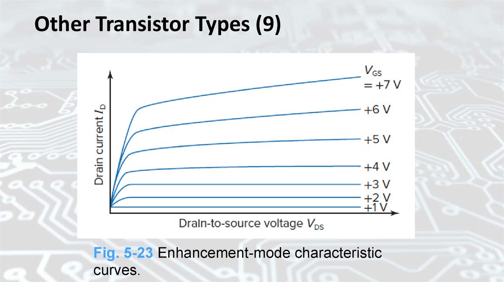
Other Transistor Types (8)Figure 5-23 shows a family of curves for an N-channel enhancementmode device. As the gate is made more positive, more electrons are
attracted into the channel area. This enhancement improves channel
conduction, and the drain current increases. When VGS = 0, the drain
current is 0. This is the cutoff region mentioned before. In Fig. 5-23, the
cutoff region lies along the VDS axis where ID is zero. The flat or nearly flat
curves are in the saturation region, and the steep vertical section is the
ohmic region. A JFET should not be operated in the enhancement mode
because the gate diode could become forward-biased, and gate current
would flow. Gate current is not desired in any type of FET. Field-effect
transistors are normally voltage-controlled.
67.
Other Transistor Types (9)Fig. 5-23 Enhancement-mode characteristic
curves.
68.
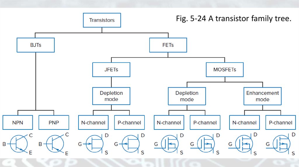
Other Transistor Types (10)Figure 5-24 shows a transistor family tree. Note that the
enhancement-mode symbols use a broken line from the source to the
drain. This is because the channel can be created or enhanced by
applying the correct gate voltage. Field-effect transistors have some
advantages over bipolar transistors that make the former attractive for
certain applications. Their gate terminal does not require any current.
This is a good feature when an amplifier with high input resistance is
needed. This is easy to understand by inspecting Ohm’s law:
Consider V to be a signal voltage supplied to an amplifier and I the
current taken by the amplifier. In this equation, as I decreases, R
increases.
69.
Fig. 5-24 A transistor family tree.70.
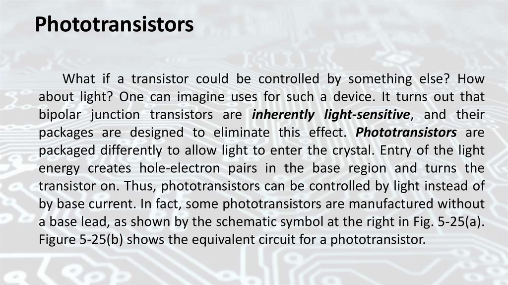
PhototransistorsWhat if a transistor could be controlled by something else? How
about light? One can imagine uses for such a device. It turns out that
bipolar junction transistors are inherently light-sensitive, and their
packages are designed to eliminate this effect. Phototransistors are
packaged differently to allow light to enter the crystal. Entry of the light
energy creates hole-electron pairs in the base region and turns the
transistor on. Thus, phototransistors can be controlled by light instead of
by base current. In fact, some phototransistors are manufactured without
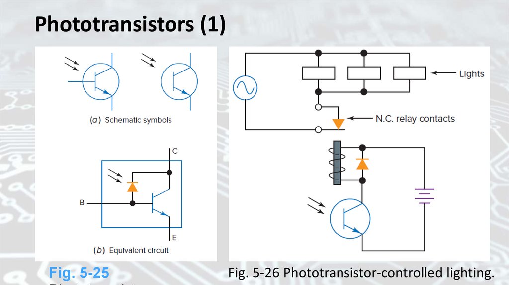
a base lead, as shown by the schematic symbol at the right in Fig. 5-25(a).
Figure 5-25(b) shows the equivalent circuit for a phototransistor.
71.
Phototransistors (1)Fig. 5-25
Fig. 5-26 Phototransistor-controlled lighting.
72.
Phototransistors (2)The collector is several volts positive with respect to the emitter. With no
light entering the package, only a small current flows. It is typically on the order
of 10 nanoamperes (nA) at room temperature. It is called the dark current.
When light does enter, it penetrates the diode depletion region and generates
carriers. The diode conducts and provides base current for the phototransistor.
The transistor has gain, so we can expect the collector current to be a great
deal larger than the current flow in the diode in Fig. 5-25(b). A typical photo
transistor might show 5 mA of collector current with a light input of 3 mW per
square centimeter.
One possible application for a phototransistor is shown in Fig. 5-26. This
circuit provides automatic lighting. With daylight conditions, the transistor
conducts and holds the normally closed (NC) contacts of the relay open. This
keeps the lights turned off. When night falls, the phototransistor dark current is
too small to hold the relay in, and the contacts close and turn on the lights.
73.
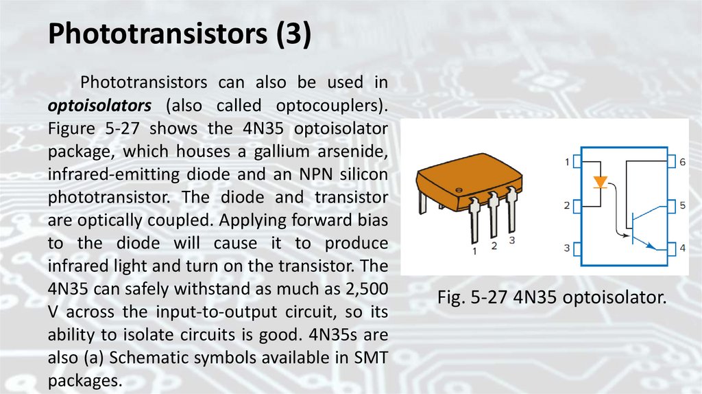
Phototransistors (3)Phototransistors can also be used in
optoisolators (also called optocouplers).
Figure 5-27 shows the 4N35 optoisolator
package, which houses a gallium arsenide,
infrared-emitting diode and an NPN silicon
phototransistor. The diode and transistor
are optically coupled. Applying forward bias
to the diode will cause it to produce
infrared light and turn on the transistor. The
4N35 can safely withstand as much as 2,500
V across the input-to-output circuit, so its
ability to isolate circuits is good. 4N35s are
also (a) Schematic symbols available in SMT
packages.
Fig. 5-27 4N35 optoisolator.
74.
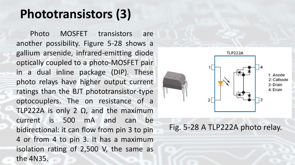
Phototransistors (3)Photo MOSFET transistors are
another possibility. Figure 5-28 shows a
gallium arsenide, infrared-emitting diode
optically coupled to a photo-MOSFET pair
in a dual inline package (DIP). These
photo relays have higher output current
ratings than the BJT phototransistor-type
optocouplers. The on resistance of a
TLP222A is only 2 Ω, and the maximum
current is 500 mA and can be
bidirectional: it can flow from pin 3 to pin
4 or from 4 to pin 3. It has a maximum
isolation rating of 2,500 V, the same as
the 4N35.
Fig. 5-28 A TLP222A photo relay.
75.
Power TransistorsTransistors can be divided into two broad categories: small-signal
devices and power devices. When they must safely handle more than 1 W,
they are in the power category. This is an arbitrary division. Accordingly, in
Table 5-1 2N2222A transistor is rated at 1.8 W. However, that rating is for a
device temperature of 25°C. When the ambient temperature is 25°C, the
rating is only 625 mW. This is because the transistor will rise in temperature
when it is dissipating power.
76.
Power Transistors (1)A 2N2222A conducting 200 mA and dropping 9 V (that’s 1.8 W) can
burn your finger if you touch it. It will be operating well above 25°C and will
fail if it operates like that for a period of time (perhaps only seconds). When
operated at 625 mW, it will still burn your finger (but not as badly) because
it will reach a case temperature of around 90°C. Compare that with a
2N6288 power transistor, which will reach a case temperature of only about
55°C when dissipating 625 mW. Looking at the two cases shown in Fig. 5-29
makes it clear why the power transistor operates cooler. The 2N6288 is
packaged in a TO-220 case, while a 2N2222A uses the TO-92.
77.
Power Transistors (2)Figure 5-29 shows that there is a significant difference in transistor case
sizes. It also shows that the power transistor has a metal tab. This tab is
often mechanically connected to a heat sink. The heat sink is designed to
conduct and transfer heat to the ambient environment, which will prevent
the transistor from failing due to overtemperature. A 2N6288 is rated at 40
W maximum dissipation, but that’s only if the heat sink maintains the case
temperature at 25°C (77°F). That is not easily done; think of Florida in
August. Power transistors are almost never operated at their maximum
ratings. Fig. 5-30 shows the power derating curve for the device.
78.
Power Transistors (3)Fig. 5-29 A small-signal transistor and a
power transistor.
Fig. 5-30 Power derating curve for a
2N6288 transistor.
79.
Power Transistors (4)Heat is one of biggest factors in the failure of electronic devices, and
that certainly includes transistors. Most have an upper temperature limit of
150°C, although some are rated at 200°C. Those are junction temperature
ratings. If you burn a finger on a transistor, consider that the junction inside
the case is a lot hotter! How hot will a transistor get? Power (dissipation)
can be determined using
Thus, as current and/or voltage increases, so does the power. This implies
limits. Look at Fig. 5-31.
80.
Fig. 5-31 Safe limits of FET operation.81.
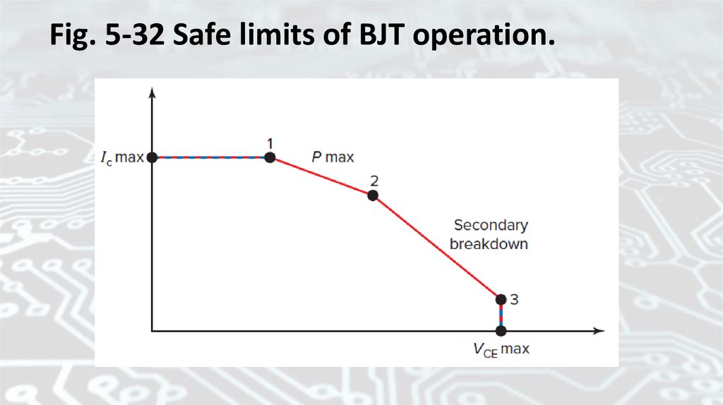
Power Transistors (5)The most obvious limits are the maximum safe current and the
maximum safe voltage. Exceeding either can damage or destroy a
transistor. The other limit is set by the product of voltage and current. Thus,
as VDS increases, ID will be less for the same power. The line between points
1 and 2 in Fig. 5-31 represents the maximum power limit for the device.
Bipolar junction transistors have an additional limitation, as shown in
Fig. 5-32.
82.
Fig. 5-32 Safe limits of BJT operation.83.
Power Transistors (6)Notice the curve between points 2 and 3. It has a steeper slope than
Pmax, which implies an additional limit on the maximum safe power. With
BJTs, higher currents and voltages can cause current flow to become
confined to a small region of the crystal. A hot spot forms, and the crystal is
damaged. This phenomenon does not exist with power FETs and is one of
the reasons that FETs have become dominant in some applications. There is
a related phenomenon called secondary breakdown or second breakdown,
but it usually does not cause as many device failures. Although BJTs are
often cheaper, power FETs are often more reliable.
Semiconductor manufacturers publish many kinds of graphs for their
devices. Fig. 5-33 shows the safe operating area for a PNP transistor. The
maximum safe transistor dissipation for this particular transistor happens to
be 7.5 W, and no operating point that falls to the right of the power curve
would be safe.
84.
Fig. 5-33 Constant power curve.85.
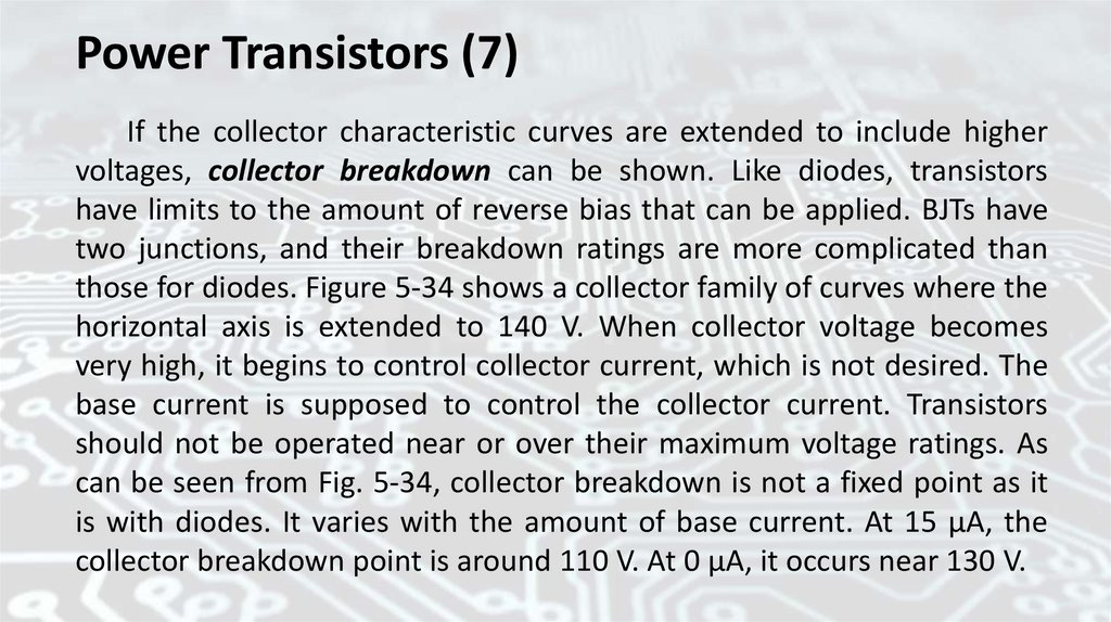
Power Transistors (7)If the collector characteristic curves are extended to include higher
voltages, collector breakdown can be shown. Like diodes, transistors
have limits to the amount of reverse bias that can be applied. BJTs have
two junctions, and their breakdown ratings are more complicated than
those for diodes. Figure 5-34 shows a collector family of curves where the
horizontal axis is extended to 140 V. When collector voltage becomes
very high, it begins to control collector current, which is not desired. The
base current is supposed to control the collector current. Transistors
should not be operated near or over their maximum voltage ratings. As
can be seen from Fig. 5-34, collector breakdown is not a fixed point as it
is with diodes. It varies with the amount of base current. At 15 μA, the
collector breakdown point is around 110 V. At 0 μA, it occurs near 130 V.
86.
Fig. 5-34 Collector breakdown.87.
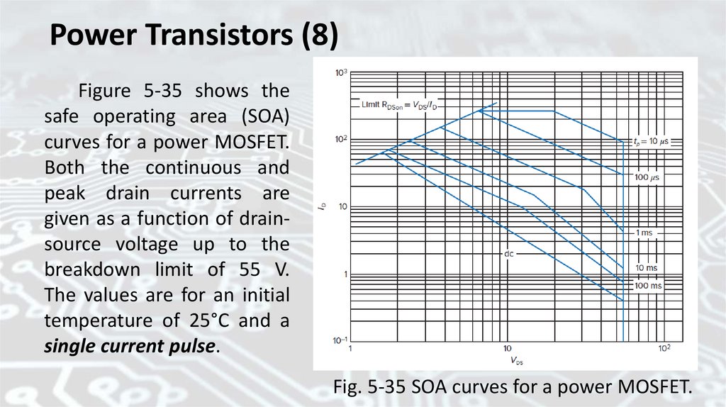
Power Transistors (8)Figure 5-35 shows the
safe operating area (SOA)
curves for a power MOSFET.
Both the continuous and
peak drain currents are
given as a function of drainsource voltage up to the
breakdown limit of 55 V.
The values are for an initial
temperature of 25°C and a
single current pulse.
Fig. 5-35 SOA curves for a power MOSFET.
88.
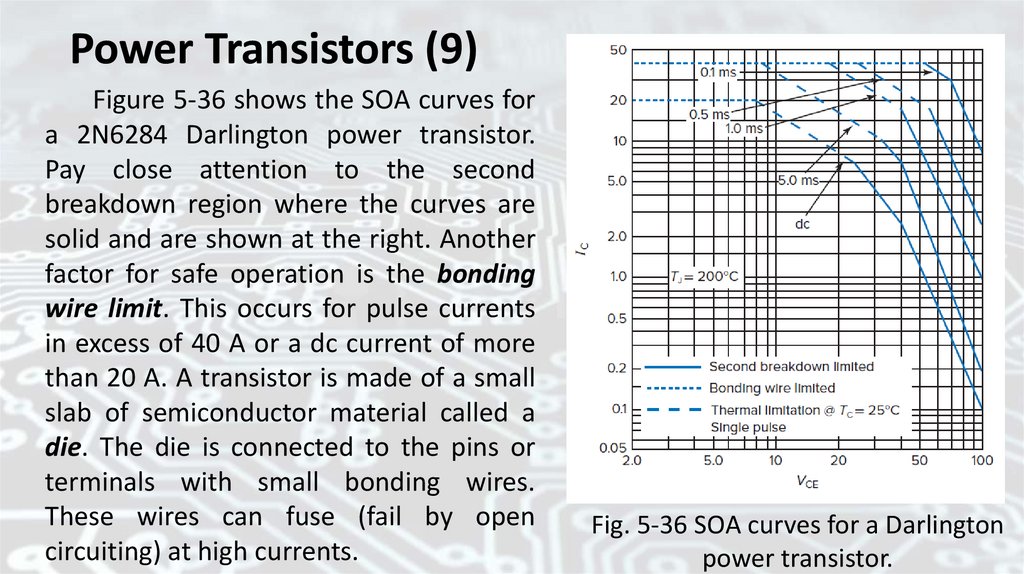
Power Transistors (9)Figure 5-36 shows the SOA curves for
a 2N6284 Darlington power transistor.
Pay close attention to the second
breakdown region where the curves are
solid and are shown at the right. Another
factor for safe operation is the bonding
wire limit. This occurs for pulse currents
in excess of 40 A or a dc current of more
than 20 A. A transistor is made of a small
slab of semiconductor material called a
die. The die is connected to the pins or
terminals with small bonding wires.
These wires can fuse (fail by open
circuiting) at high currents.
Fig. 5-36 SOA curves for a Darlington
power transistor.
89.
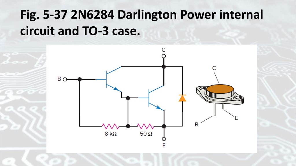
Power Transistors (10)Figure 5-37 shows the internal circuit for a 2N6284 Darlington power
transistor. The case is the TO-3 style, which is similar to the TO-204. Notice that
the emitter of the left-hand transistor controls (feeds into) the base of the righthand transistor. The current gain from the B terminal to the C terminal is
approximately equal to the product of both transistor gains. If each transistor
has a current gain of 50:
hFE(both) = hFE(1) × hFE(2) = 50 × 50 = 2,500
The high current gain of Darlingtons makes them easy to drive. The next
section shows how four of them can be used to control a stepper motor.
90.
Fig. 5-37 2N6284 Darlington Power internalcircuit and TO-3 case.
91.
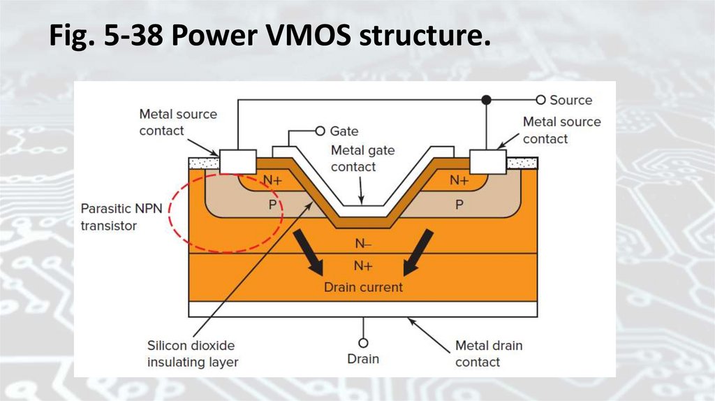
Power Transistors (11)In addition to extra components being placed inside transistor cases,
there can be parasitic components. Figure 5-38 shows the internal
structure of a power vertical metallic oxide semiconductor (VMOS)
transistor. The name derives from the V-shaped channel. If the parasitic
BJT turns on, it cannot be turned off because the gate has no control over
it. This phenomenon is known as latchup, which can lead to device
destruction. The parasitic BJT might be turned on by a voltage drop across
the P-type body region. To avoid latchup, the body and source are typically
short-circuited within the device package.
92.
Fig. 5-38 Power VMOS structure.93.
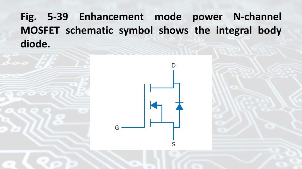
Power Transistors (12)Figure 5-39 shows the schematic symbol for the transistor shown in
Fig. 5-38. The gate is insulated from the N channel. Note that the
schematic symbol shows no electrical connection between the G
terminal and the D or S terminal. Also note the diode across the S and D
terminals. This is the integral body diode that can be seen by looking
closely at Fig. 5-38. There is a parasitic diode between the source (which
forms the P portion of the diode) and the drain (which forms the N
portion).
The body diode is convenient in circuits that require a path for any
possible reverse drain current (often called the freewheeling current).
Inductive loads store energy, and when a MOSFET turns off, the body
diode can provide a safe path for the discharge current.
94.
Fig. 5-39 Enhancement mode power N-channelMOSFET schematic symbol shows the integral body
diode.
95.
Power Transistors (13)Figure 5-40 shows the VDS versus ID characteristic curves for an
enhancement mode power MOSFET. The drain current is definitely
enhanced by the gate voltage. As you can see, the current becomes high
for gate voltages greater than 4 V. For much lower gate voltages, such as
those near 0 V, the transistor will be off. As we learned before,
enhancement mode transistors are normally off and must be turned on
by applying gate voltage. Note that the specified pulse duration is short
and specified at a very small duty cycle. Otherwise, the transistor would
be destroyed by heat.
96.
Fig. 5-40 Power enhancement-type MOSFETcharacteristic curves
97.
Power Transistors (14)With high-power transistors, the drive requirements become
important. Both BJT and MOSFET transistors can handle high power.
Although BJTs can fail due to second breakdown, they are still good
choices for some applications. MOSFETs are voltage-driven or voltagecontrolled. This is an advantage in power devices. The driver only has
to supply a changing voltage. In BJTs, the driver has to supply current
and voltage. Darlingtons are easier to drive but also can fail from
second breakdown, so MOSFETs might be preferred. However,
MOSFETs still require some drive power due to their input capacitance.
In switching circuits with fast rise times or in high-frequency designs,
the capacitance means there will have to be input current. Recall that
rapid voltage change causes significant current in capacitive circuits.
98.
Power Transistors (15)Yet another advantage of MOSFETs is that they don’t have a
problem with minority carrier storage that can limit how quickly a
transistor can be turned off. In switching circuits, when the transistors
are on, they are turned on hard (they are said to be saturated). To turn
off an NPN transistor, for example, all the minority electrons in the
base have to be cleared out before the device shuts off. There are lots
of those in a saturated BJT. PNPs have the same issue.
Power BJTs are not as popular as they once were. They are still a
viable technology, but MOSFETs are often better even though they may
cost a bit more.
99.
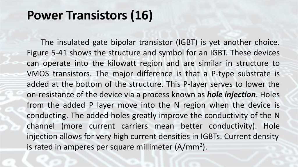
Power Transistors (16)The insulated gate bipolar transistor (IGBT) is yet another choice.
Figure 5-41 shows the structure and symbol for an IGBT. These devices
can operate into the kilowatt region and are similar in structure to
VMOS transistors. The major difference is that a P-type substrate is
added at the bottom of the structure. This P-layer serves to lower the
on-resistance of the device via a process known as hole injection. Holes
from the added P layer move into the N region when the device is
conducting. The added holes greatly improve the conductivity of the N
channel (more current carriers mean better conductivity). Hole
injection allows for very high current densities in IGBTs. Current density
is rated in amperes per square millimeter (A/mm2).
100.
Power Transistors (17)Semiconductor manufacturers
such
as
ON
SemiconductorTM sell unpackaged dies such as the
NGTD21T65F2, which is
about 20 mm2 and rated at
200 A. With a high current
density, a given device size
can support more current
flow. High current densities
are important for power
transistors.
Fig. 5-41 IGBT transistor schematic symbol
and structure.
101.
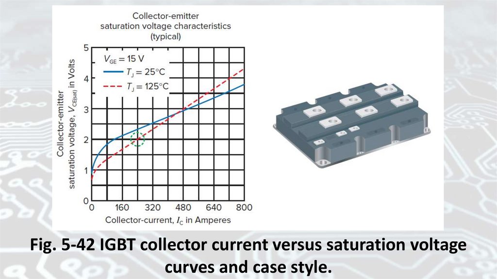
Power Transistors (18)Figure 5-42 shows the saturation curves and the case (package) for one
IGBT. Saturation curves are used to predict how a device behaves when it is
turned on very hard (saturated). The elected operating point in the red circle
represents an RCE value of only 8.33 mΩ:
RCE = VCE/IC = 2 V/240 A = 8.33 mΩ
In switching circuits, the main idea is to keep the power dissipated in a
switch as low possible. Here is a quick review of how power is calculated:
1. P = V × I (the definition equation)
2. P = I2R (as RCE or RDS approaches 0, so does the power)
3. P = V2/R (as VSAT approaches 0, so does the power)
Equation 2 above comes into play with IGBTs and MOSFETs, and equation 3
comes into play with BJTs. VSAT, the collector saturation voltage, should be
as low as possible in switches. It is typically less than 0.4 V in power BJTs.
102.
Fig. 5-42 IGBT collector current versus saturation voltagecurves and case style.
103.
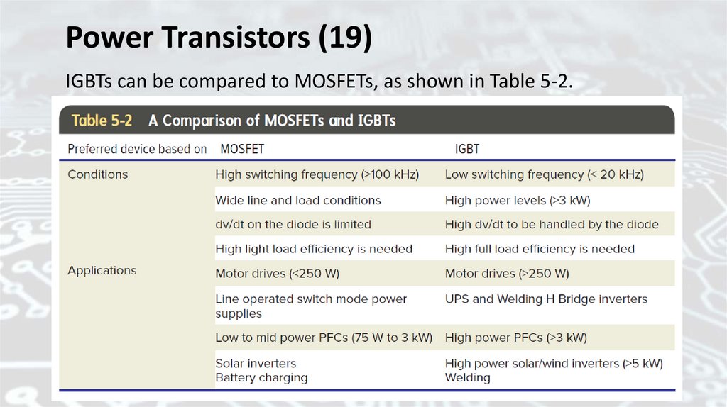
Power Transistors (19)IGBTs can be compared to MOSFETs, as shown in Table 5-2.
104.
Power Transistors (20)The thermal model of a transistor is shown in Fig. 5-43. Heat flow can
be modeled as current flow. The model shows there are three thermal
resistances: the thermal resistance of the junction to the case (RθJC), the
case to the heat sink (RθCS), and the heat sink to the ambient (RθSA). RθJC is
due to the thermal resistance of the material used to mount the die to the
case (solder). As the chip heats, the heat will move on to the case through
the equivalent resistance (RθJC). RθCS is the resistance for heat flow from
the transistor case to the heat sink. Note that silicon grease and a mica
washer are sometimes used to lower RθCS. RθSA is the resistance for heat
flow from the case to the ambient environment.
105.
Power Transistors (21)Designers may have to
choose a large metal heat
sink or use fan cooling to
reduce
that
resistance.
Knowing the total resistance
will allow you to calculate the
total temperature difference
just as total voltage can be
calculated for a series
electrical circuit when the
flow is known.
Fig. 5-43 Thermal equivalent circuit.
106.
Power Transistors (22)The thermal model shown in Fig. 5-43 also shows capacitors; these
model thermal capacitance. Thermal capacitance is equivalent to thermal
mass. It takes time to charge a capacitor, and it takes time to raise or
lower temperature based on thermal mass. People who cook know about
thermal mass. It takes a lot longer to bring a quart of water to a boil than
to do the same with a cup. Thermal mass is important in pulse circuits
(they have smaller duty cycles). In a pulse circuit, the total thermal mass
will help limit how hot it gets.
107.
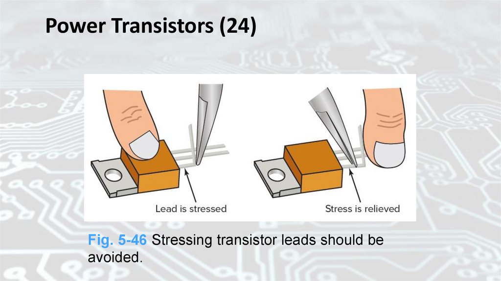
Power Transistors (23)The handling of power devices is also important. Figure 5-46 shows
that lead bending must be done in a way that does not stress the device.
Power transistors fail more often than small-signal transistors. The
former normally run hot, which shortens the life. Technicians typically
replace more power transistors than they do small-signal transistors.
Usually, an exact replacement is the best bet. If a substitution is required,
the same type and polarity are mandated. The maximum ratings for
voltage, current, and power should not be exceeded. Sometimes
manufacturers recommend an upgraded device. It might be possible to
adapt a different type but safety and reliability could be compromised;
therefore, this practice is not advised. When a power device is replaced,
the mounting hardware and possibly the application of a special thermal
compound (such as silicon grease) are important considerations.
108.
Power Transistors (24)Fig. 5-46 Stressing transistor leads should be
avoided.
109.
Transistors as SwitchesThe term “solid-state switch” refers to a switch that has no moving
parts. Transistors lend themselves for use as switches because they can be
turned on with a base current or a gate voltage to produce a low resistance
path (the switch is on), or they can be turned off by removing the base
current or the gate voltage to produce a high resistance (the switch is off).
They are very widely applied because they are small, quiet, inexpensive,
reliable, capable of highspeed operation, easy to control, and relatively
efficient.
Figure 5-47 shows a typical application. It is a computer-controlled
battery conditioner. It is used to determine the condition of rechargeable
batteries. It automatically cycles a battery from charge to discharge to
charge while it monitors both battery voltage and temperature. Modern
rechargeable batteries are often expensive. Many require specific charging
methods for maximum life.
110.
Fig. 5-47 Computer-controlled battery conditioner111.
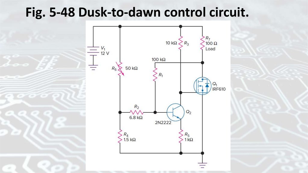
Transistors as Switches (1)Figure 5-48 is a dusk-to-dawn controller without a mechanical relay
or a phototransistor. This circuit uses a light-dependent resistor (LDR) as a
sensor along with two transistors that act as switches. The LDR is made of
a material that conducts better when exposed to light. When the sun
comes up, Q2 turns on, and its collector voltage drops to some low value,
as does the gate voltage of Q1. The load is now off (lights off at dawn).
When darkness comes, the resistance goes up and Q2 turns off. With Q2
off, its collector voltage goes high, as does the gate of Q1, turning it on;
the load is now on (lights go on at dusk).
112.
Fig. 5-48 Dusk-to-dawn control circuit.113.
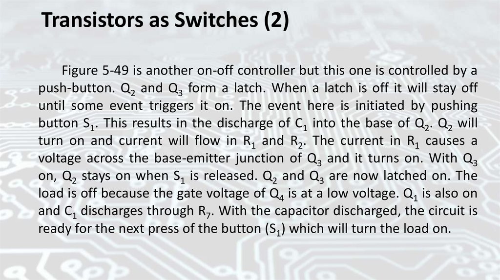
Transistors as Switches (2)Figure 5-49 is another on-off controller but this one is controlled by a
push-button. Q2 and Q3 form a latch. When a latch is off it will stay off
until some event triggers it on. The event here is initiated by pushing
button S1. This results in the discharge of C1 into the base of Q2. Q2 will
turn on and current will flow in R1 and R2. The current in R1 causes a
voltage across the base-emitter junction of Q3 and it turns on. With Q3
on, Q2 stays on when S1 is released. Q2 and Q3 are now latched on. The
load is off because the gate voltage of Q4 is at a low voltage. Q1 is also on
and C1 discharges through R7. With the capacitor discharged, the circuit is
ready for the next press of the button (S1) which will turn the load on.
114.
Fig. 5-49 Push button control.115.
Transistors as Switches (3)Figure 5-50 shows another application for transistor switches. Stepper
motors can be used in applications where tight control of speed and
position is required. Such applications include computer disk drives,
numerically controlled (automated) lathes and milling machines, and
automated surface mount assembly lines. The shaft of a stepper motor
moves in defined increments such as 1, 2, or 5 degrees per step. If a
motor is a 1-degree type, then 180 pulses will move the shaft exactly onehalf turn. As Fig. 5-50(b) shows, four groups of pulses are required with
this particular motor.
116.
Transistors as Switches (4)A computer or a microprocessor sends precisely timed waveforms to
the switching transistors to control the four motor leads: W, X, Y, and Z in
Fig. 5-50(a). The control waveforms are shown as phases A, B, C, and D in
Fig. 5-50(b); note that they are rectangular. This is typical when transistors
are used as switches. They are either on or off (high or low). Figure 550(d) shows that power MOSFETs can also be used to control stepper
motors.
117.
Fig. 5-50(a) Control of stepper motors.118.
Fig. 5-50(b-d) Control of stepper motors.119.
Transistors as Switches (5)Figure 5-51 shows control of a dc motor. The circuit achieves on-off
control by applying a +5-V drive signal to Q3 to turn the motor on and a
0-V drive signal to turn the motor off. Also, pulse-width modulation
(PWM) can be used to control the speed of the motor over a wide range.
Circuits such as the one in Fig. 5-51 are widely used, since power
FETs are inexpensive, can have very low on-resistance, and operate
efficiently at high frequencies (which makes them attractive in PWM
applications).
120.
Fig. 5-51 Control of a dc motor.121.
Transistors as Switches (6)So far, the transistor switches discussed have been used for turning
loads on and off. There is another category called an analog switch,
which is used to control the flow of analog signals. For example, analog
switches can be used to select among different signal sources in a sound
system (tuner, MP3 player, CD, DVD, and so on). Generally, they are
offered as integrated circuits, but it is possible to use enhancementmode transistors to achieve this function. Figure 5-52 shows an example
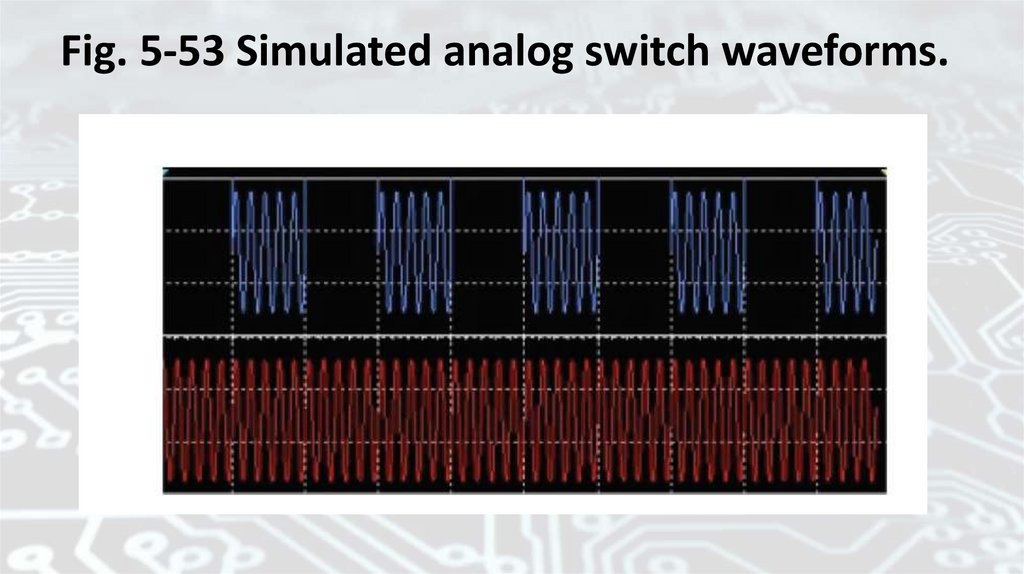
circuit, and Fig. 5-53 shows example waveforms.
In Fig. 5-52, the switching transistor is a 2N7002, which is an Nchannel, enhancement-mode MOSFET. This device shows a low
resistance from source to drain when a positive voltage is applied to the
gate terminal.
122.
Transistors as Switches (7)The signal source is connected to the source terminal, and the
drain terminal provides the output signal. The control turns the
transistor on by applying a voltage to the gate. Figure 5-53 shows
the input signal in red and the output signal in blue. Note that the
output signal is being switched on and off. The control signal in
this case is a square wave. When it goes positive, the switch is on
and the sine wave appears at the output. The input signal and the
output signal in Figs. 5-52 and 5-53 are of the same amplitude. In other
words, this is a switch and not a amplifier.
123.
Fig. 5-52 MOSFET analog switch.124.
Fig. 5-53 Simulated analog switch waveforms.125.
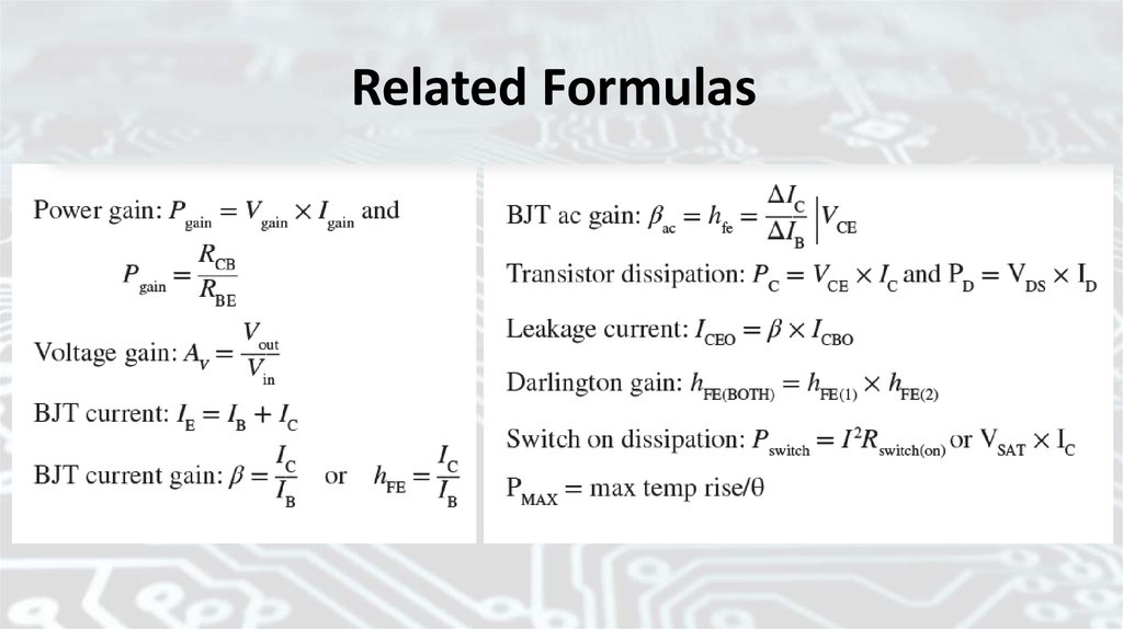
Summary1. Gain is the basic function of any amplifier.
2. Gain can be calculated using voltage, current, or power. In all cases, the
units cancel and gain is simply a number.
3. Power gain is the product of voltage gain and current gain.
4. The term voltage amplifier is often used to describe a small-signal
amplifier.
5. The term power amplifier is often used to describe a large-signal
amplifier.
6. Bipolar junction transistors are manufactured in two polarities: NPN
and PNP. The NPN types are more widely applied.
7. In a BJT, the emitter emits the carriers, the base is the control region,
and the collector collects the carriers.
126.
Summary (1)8. The schematic symbol of an NPN transistor shows the emitter lead
arrow Not Pointing iN.
9. Normal operation of a BJT requires that the collector-base junction be
reverse-biased and the base-emitter junction be forward-biased.
10. Most of the current carriers coming from the emitter cannot find
carriers in the base region with which to combine. This tends to make the
base current much less than the other currents.
11. The base is very narrow, and the collector bias attracts the carriers
coming from the emitter. This tends to make the collector current almost
as high as the emitter current.
12. Beta (β), or hFE, is the current gain from the base terminal to the
collector terminal. The value of β varies considerably, even among devices
with the same part number.
127.
Summary (2)13. Base current controls collector current and emitter current.
14. Emitters of PNP transistors produce holes. Emitters of NPN transistors
produce electrons.
15. A collector characteristic curve is produced by plotting a graph of IC
versus VCE with IB at some fixed value.
16. Collector voltage has only a small effect on collector current over most
of the operating range.
17. A power curve can be plotted on the graph of the collector family to
show the safe area of operation.
18. Collector dissipation is the product of collector-emitter voltage and
collector current.
19. Germanium transistors require a base-emitter bias of about 0.2 V to
turn on. Silicon units need about 0.6 V.
128.
Summary (3)20. Silicon transistors are much more widely used than germanium
transistors.
21. Substitution guides provide the technician with needed information
about solid-state devices.
22. The physical characteristics of a part can be just as important as the
electrical characteristics.
23. Transistors can be tested with curve tracers, dynamic testers,
ohmmeters, and with various in-circuit checks.
24. Most transistors fail suddenly and completely. One or both PN
junctions may short or open.
25. An analog ohmmeter can check both junctions, identify polarity,
identify leads, check gain, indicate leakage, and may even identify the
transistor material.
129.
Summary (4)26. Leakage current ICEO is β times larger than ICBO.
27. Phototransistors are biased on with light.
28. Phototransistors can be packaged with LEDs to form devices called
optoisolators or optocouplers.
29. Bipolar transistors (NPN and PNP) use both holes and electrons for
conduction.
30. Unipolar transistors (N-channel and P-channel types) use either
electrons or holes for conduction.
31. A BJT is a normally off device. It is turned on with base current.
32. A JFET is a normally on device. It is turned off with gate voltage. This is
called the depletion mode.
33. A MOSFET uses an insulated gate structure. Manufacturers make both
depletion-type and enhancement-type MOSFETs.
130.
Summary (5)34. An enhancement-mode MOSFET is a normally off device. It is turned
on by gate voltage.
35. Field-effect transistors have a very high input resistance.
36. The abbreviations VFET and VMOS are used to refer to power fieldeffect transistors that have a vertical flow of current from source to drain.
37. Power FETs do not have some of the limitations of power bipolar
transistors. The FETs are voltage-controlled, they are faster (no minoritycarrier storage), they do not exhibit thermal runaway, and they are not
prone to secondary breakdown.
38. Power FETs operate in the enhancement mode.
131.
Summary (6)39. Transistors that are controlled by light are useful for applications such
as dusk-to-dawn circuits.
40. Combining LEDs and transistors in the same package provides
functions such as optoisolators and photo relays.
41. When a bipolar junction transistor is operated as a switch, there is
going to be either no base current or a lot of base current.
42. A switching transistor is either turned on hard (saturated) or is off.
132.
Summary (7)43. Ideally, switching is very efficient since an open switch shows no
current for zero power dissipation, and a closed switch shows no voltage
drop, which is another case of zero power dissipation.
44. In switching circuits, the control waveforms are often rectangular.
45. When inductive loads are being switched, some sort of protection
device or circuit is needed because of the CEMF generated by the
inductance.
46. The thermal resistance unit called θ has a dimension of °C/W.
47. Circuits with hysteresis have two trip points.