")


")


")


.")


 Электроника
Похожие презентации:


Field-effect transistor (FET). Junction field-effect transistor (JFET)
1.
Course: El 2207: ElectronicsCourse Instructor: assis-prof. Alnura Orazgaliqyzy Omarbekova
Assistant: lecturer Madina Zhanatovna Konyrova
email: a.omarbekova@iitu.kz, room 409
konyrova.madina0305@gmail.com, room 409
2. Introduction (FET)
Field-effect transistor (FET) are importantdevices such as BJTs
Also used as amplifier and logic switches
Types of FET:
JFET (junction field-effect transistor)
MOSFET (metal-oxide-semiconductor field-effect
transistor)
What is the difference between JFET and
MOSFET?
3. Current-controlled amplifiers
4. Voltage-controlled amplifiers
5. Introduction.. (Advantages of FET)
High input impedance (M )(Linear AC amplifier system)
Temperature stable than BJT
Smaller than BJT
Can be fabricated with fewer processing
BJT is bipolar – conduction both hole and
electron
FET is unipolar – uses only one type of current
carrier
Less noise compare to BJT
Usually use as logic switch
6. Disadvantages of FET
Easy to damage compare to BJT???
7. Junction field-effect transistor..
There are 2 types of JFETn-channel JFET
p-channel JFET
Three Terminal
gate: as in the “gate” keeper of the current
source: the source of the current
drain: the destination of the current
8. Junction field-effect transistor (JFET)
9.
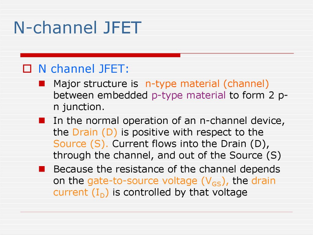
N-channel JFETN channel JFET:
Major structure is n-type material (channel)
between embedded p-type material to form 2 pn junction.
In the normal operation of an n-channel device,
the Drain (D) is positive with respect to the
Source (S). Current flows into the Drain (D),
through the channel, and out of the Source (S)
Because the resistance of the channel depends
on the gate-to-source voltage (VGS), the drain
current (ID) is controlled by that voltage
10. N-channel JFET..
11.
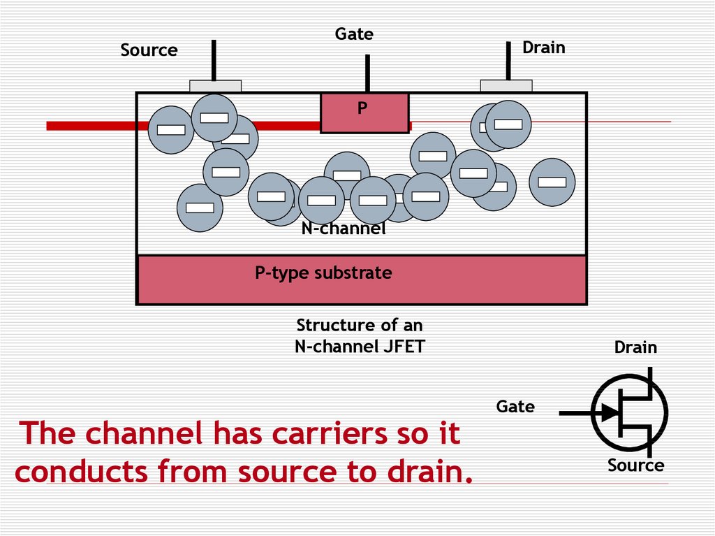
SourceGate
Drain
P
N-channel
P-type substrate
Structure of an
N-channel JFET
The channel has carriers so it
conducts from source to drain.
Drain
Gate
Source
12.
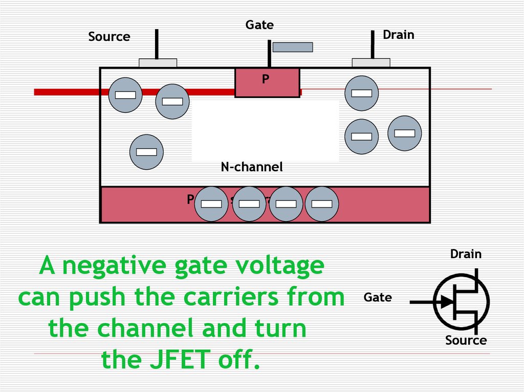
SourceGate
Drain
P
N-channel
P-type substrate
A negative gate voltage
can push the carriers from
the channel and turn
the JFET off.
Drain
Gate
Source
13.
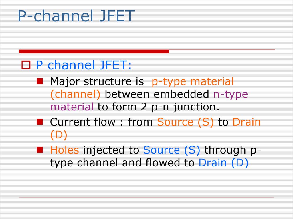
P-channel JFETP channel JFET:
Major structure is p-type material
(channel) between embedded n-type
material to form 2 p-n junction.
Current flow : from Source (S) to Drain
(D)
Holes injected to Source (S) through ptype channel and flowed to Drain (D)
14. P-channel JFET..
15.
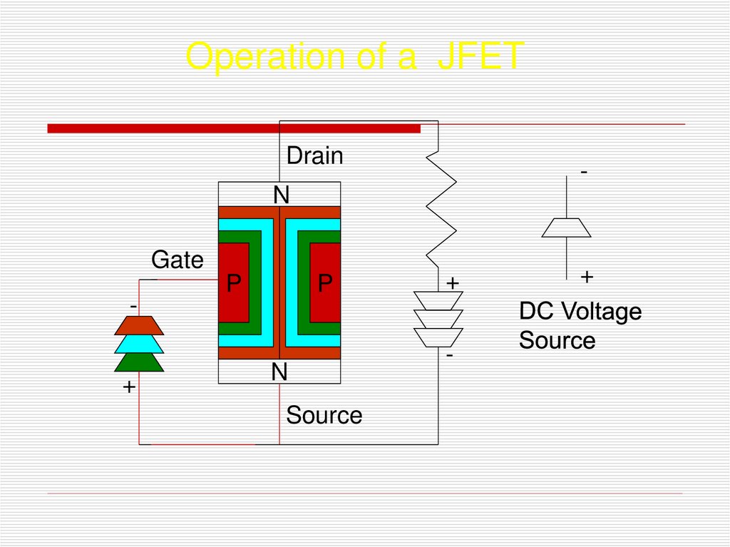
Operation of a JFETDrain
-
N
Gate
+
P
P
N
Source
+
-
+
16. Water analogy for the JFET control mechanism
17. JFET Characteristic Curve
To start, suppose VGS=0Then, when VDS is increased, ID increases.
Therefore, ID is proportional to VDS for small
values of VDS
For larger value of VDS, as VDS increases, the
depletion layer become wider, causing the
resistance of channel increases.
After the pinch-off voltage (Vp) is reached, the ID
becomes nearly constant (called as ID maximum,
IDSS-Drain to Source current with Gate Shorted)
18. ID versus VDS for VGS = 0 V.
JFET Characteristic Curve19. JFET for VGS = 0 V and 0<VDS<|Vp|
JFET for VGS = 0 V and 0<VDS<|Vp|Channel
becomes
narrower as
VDS is
increased
20. Pinch-off (VGS = 0 V, VDS = VP).
21. Application of a negative voltage to the gate of a JFET.
22.
JFET Characteristic Curve..For negative values of VGS, the gate-to-channel
junction is reverse biased even with VDS=0
Thus, the initial channel resistance is higher (in which
the initial slope of the curves is smaller for values of
VGS closer to the pinch-off voltage (VP)
The resistance value is under the control of VGS
If VGS is less than pinch-off voltage, the resistance
becomes an open-circuit ;therefore the device is in
cutoff (VGS=VGS(off) )
The region where ID constant – The saturation/pinchoff region
The region where ID depends on VDS is called the
linear/triode/ohmic region
23.
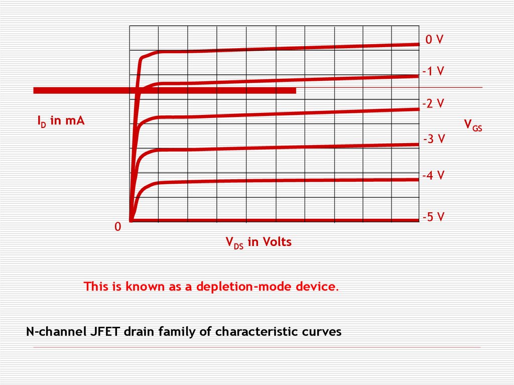
0V-1 V
-2 V
ID in mA
-3 V
-4 V
-5 V
0
VDS in Volts
This is known as a depletion-mode device.
N-channel JFET drain family of characteristic curves
VGS
24. n-Channel JFET characteristics curve with IDSS = 8 mA and VP = -4 V.
JFET Characteristic Curve25. p-Channel JFET
26. p-Channel JFET characteristics with IDSS = 6 mA and VP = +6 V.
27. Characteristics for n-channel JFET
28. Characteristics for p-channel JFET
++
+
P
29. Operation of n-channel JFET
JFET is biased with two voltage sources:VDD
VGG
VDD generate voltage bias between Drain (D)
and Source (S) – VDS
VDD causes drain current, ID flows from Drain
(D) to Source (S)
VGG generate voltage bias between Gate (G)
and Source (S) with negative polarity source is
connected to the Gate Junction (G) – reversebiases the gate; therefore gate current, IG = 0.
VGG is to produce depletion region in N channel
so that it can control the amount of drain
current, ID that flows through the channel
30. Transfer Characteristics
The input-output transfer characteristic ofthe JFET is not as straight forward as it is
for the BJT. In BJT:
IC= IB
which is defined as the relationship
between IB (input current) and IC (output
current).
31. Transfer Characteristics..
In JFET, the relationship between VGS (inputvoltage) and ID (output current) is used to
define the transfer characteristics. It is called
as Shockley’s Equation:
VGS
ID = IDSS 1
VP
2
VP=VGS (OFF)
The relationship is more complicated (and not
linear)
As a result, FET’s are often referred to a
square law devices
32. Transfer Characteristics…
Defined by Shockley’s equation:V
GS
I D I DSS 1
VGS
(
off
)
2
VP VGS ( off )
Relationship between ID and VGS.
Obtaining transfer characteristic curve axis
point from Shockley:
When VGS = 0 V, ID = IDSS
When VGS = VGS(off) or Vp, ID = 0 mA
33. Transfer Characteristics
JFET Transfer Characteristic CurveJFET Characteristic Curve
34. DC JFET Biasing
Just as we learned that the BJT must bebiased for proper operation, the JFET also
must be biased for operation point (ID, VGS,
VDS)
In most cases the ideal Q-point will be at
the middle of the transfer characteristic
curve, which is about half of the IDSS.
3 types of DC JFET biasing configurations :
Fixed-bias
Self-bias
Voltage-Divider Bias
35. Fixed-bias
+VDD
RD
C2
+
VDS
_
C1
RG
+
+ VGS
_
+
Vout
Vin
_
VGG
_
Fixed-bias
Use two
voltage
sources: VGG,
VDD
VGG is reversebiased at the
Gate – Source
(G-S)
terminal, thus
no current
flows through
RG (IG = 0).
36. Fixed-bias..
DC analysisAll capacitors replaced with open-circuit
VDD
RD
+
VDS
_
RG
+ VGS
_
Loop 1
VGG
37. Fixed-bias…
1.Input Loop
By using KVL at loop 1:
VGG + VGS = 0
VGS = - VGG
For graphical solution, use VGS = - VGG to draw the load
line
For mathematical solution, replace VGS = -VGG in Shockley’s
Eq. ,therefore:
VGS
I D I DSS 1
VGS ( off )
2
I DSS 1 VGG
VGS ( off )
2
2.
Output loop
- VDD + IDRD + VDS = 0
VDS = VDD – IDRD
3.
Then, plot transfer characteristic curve by using Shockley’s
Equation
38.
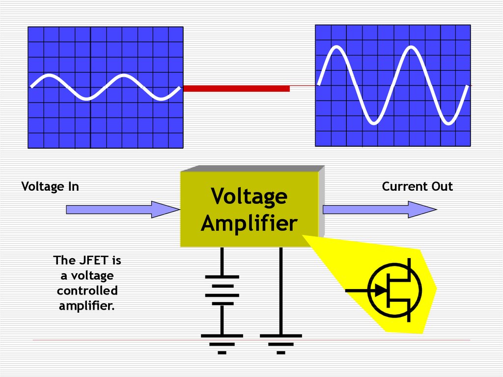
Voltage InThe JFET is
a voltage
controlled
amplifier.
Voltage
Amplifier
Current Out