


 Электроника
Похожие презентации:


")


")
Voltage Sephiroth Kwon GRMA
1.
VoltageSephiroth Kwon
GRMA
20-05-2009
2.
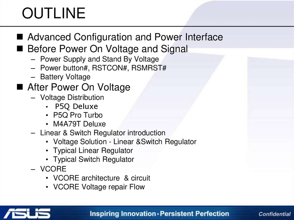
OUTLINEAdvanced Configuration and Power Interface
Before Power On Voltage and Signal
– Power Supply and Stand By Voltage
– Power button#, RSTCON#, RSMRST#
– Battery Voltage
After Power On Voltage
– Voltage Distribution
• P5Q Deluxe
• P5Q Pro Turbo
• M4A79T Deluxe
– Linear & Switch Regulator introduction
• Voltage Solution - Linear &Switch Regulator
• Typical Linear Regulator
• Typical Switch Regulator
– VCORE
• VCORE architecture & circuit
• VCORE Voltage repair Flow
3.
Advanced Configurationand
Power Interface
4.
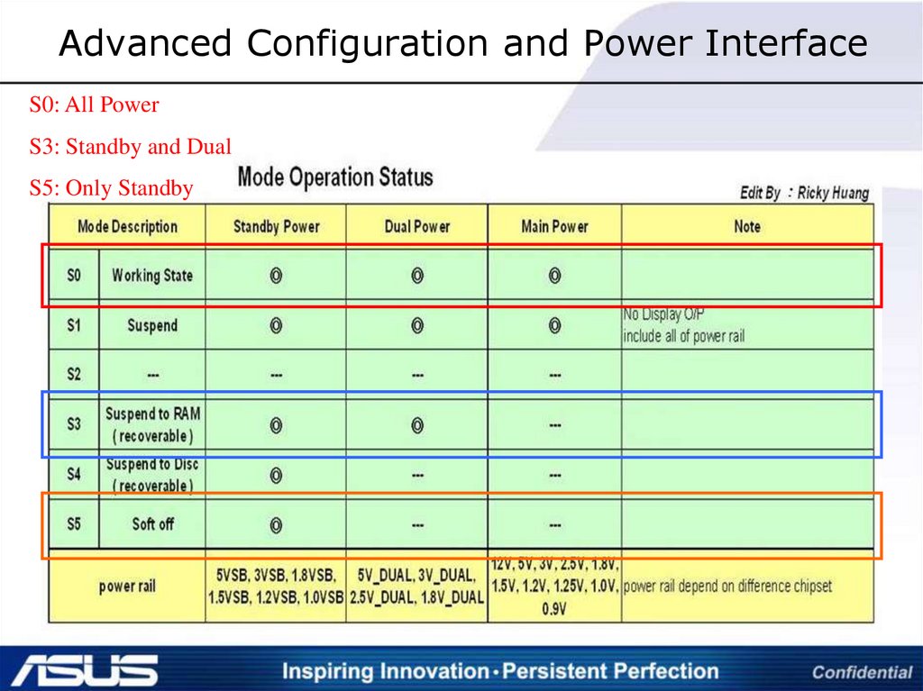
Advanced Configuration and Power InterfaceS0: All Power
S3: Standby and Dual
S5: Only Standby
5.
Before Power OnVoltage and Signal
6.
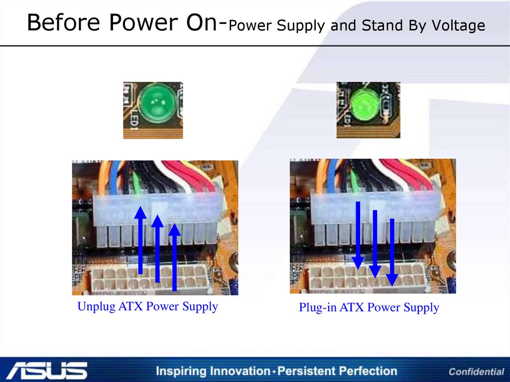
Before Power On-Power Supply and Stand By VoltageUnplug ATX Power Supply
Plug-in ATX Power Supply
7.
Before Power On-Power Supply and Stand By Voltage3.3V *
11
-12V
12
2
3.3V *
GND
COM
13
3
GND
COM
PS-ON #
14
4
5V
GND
COM
15
5
GND
COM
GND
COM
16
6
5V
GND
COM
17
7
GND
COM
-5V
18
8
PW-OK
5V
19
9
5VSB
5V
20
10
12V
1
* optional
3.3V *
5VSB
is a standby voltage that may
be used to power circuits that require
power input during the powered down
state of the power rails.
PS-ON# is an active low signal that
turns on all of the main power rails
including 3.3V, 5V, -5V, 12V, and -12V
power rails.
8.
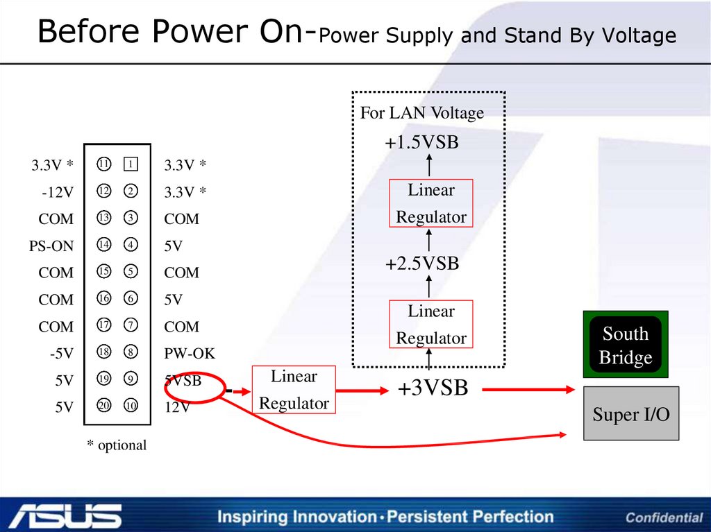
Before Power On-Power Supply and Stand By VoltageFor LAN Voltage
+1.5VSB
3.3V *
11
1
3.3V *
-12V
12
2
3.3V *
Linear
COM
13
3
COM
Regulator
PS-ON
14
4
5V
COM
15
5
COM
COM
16
6
5V
COM
17
7
-5V
18
8
PW-OK
5V
19
9
5VSB
5V
20
10
* optional
+2.5VSB
Linear
COM
12V
Regulator
Linear
Regulator
South
Bridge
+3VSB
Super I/O
9.
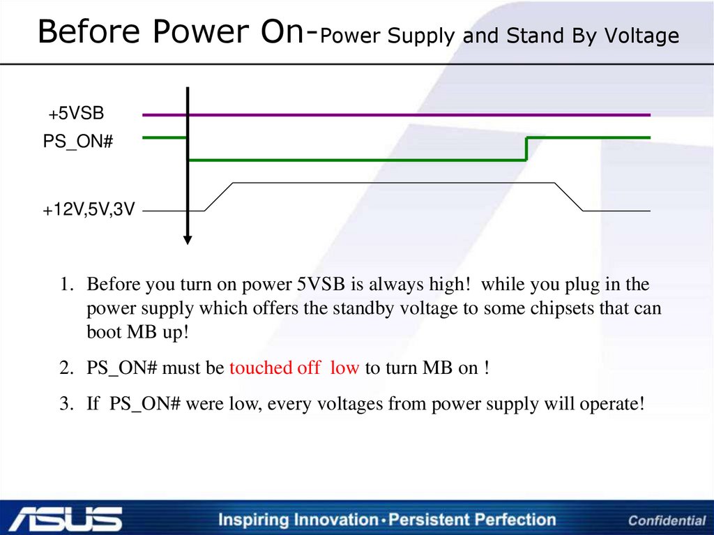
Before Power On-Power Supply and Stand By Voltage+5VSB
PS_ON#
+12V,5V,3V
1. Before you turn on power 5VSB is always high! while you plug in the
power supply which offers the standby voltage to some chipsets that can
boot MB up!
2. PS_ON# must be touched off low to turn MB on !
3. If PS_ON# were low, every voltages from power supply will operate!
10.
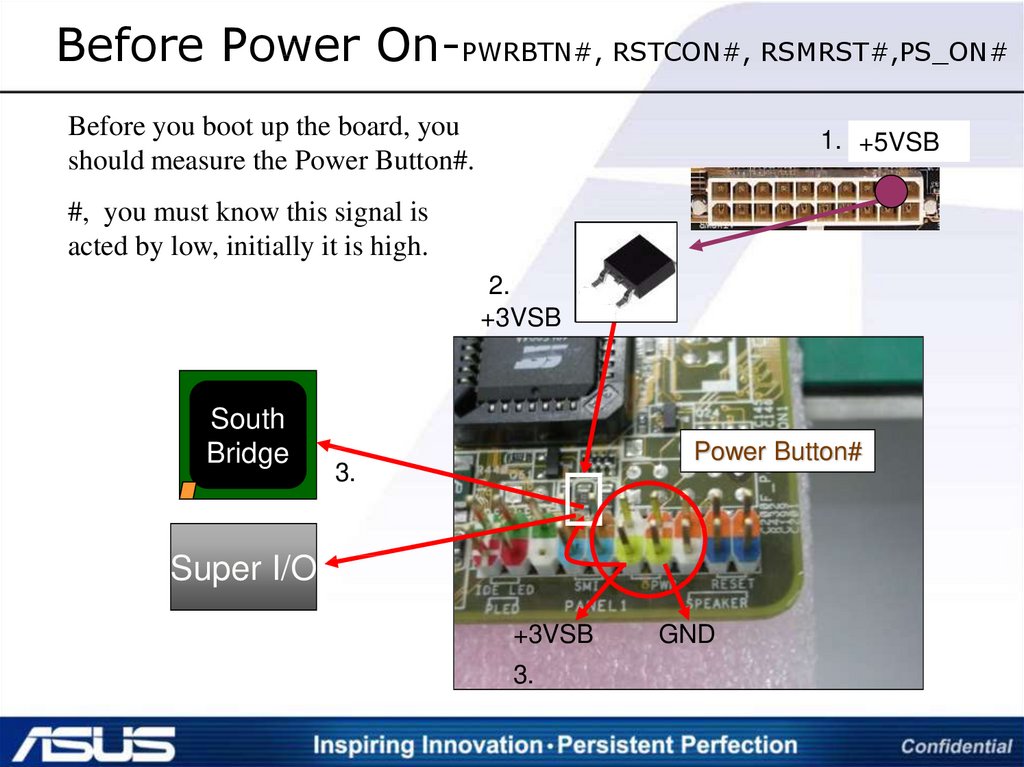
Before Power On-PWRBTN#, RSTCON#, RSMRST#,PS_ON#Before you boot up the board, you
should measure the Power Button#.
1. +5VSB
#, you must know this signal is
acted by low, initially it is high.
2.
+3VSB
South
Bridge
Power Button#
3.
Super I/O
+3VSB
3.
GND
11.
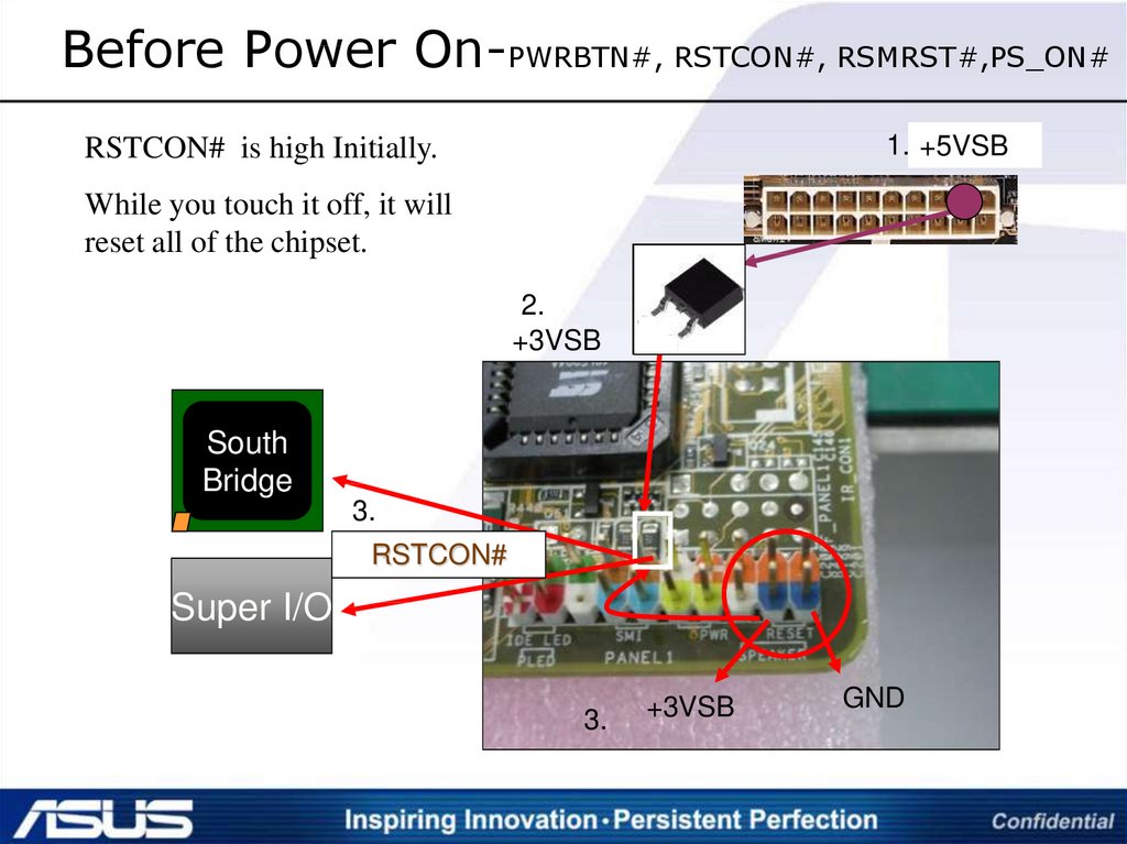
Before Power On-PWRBTN#, RSTCON#, RSMRST#,PS_ON#1. +5VSB
RSTCON# is high Initially.
While you touch it off, it will
reset all of the chipset.
2.
+3VSB
South
Bridge
3.
RSTCON#
Super I/O
3.
+3VSB
GND
12.
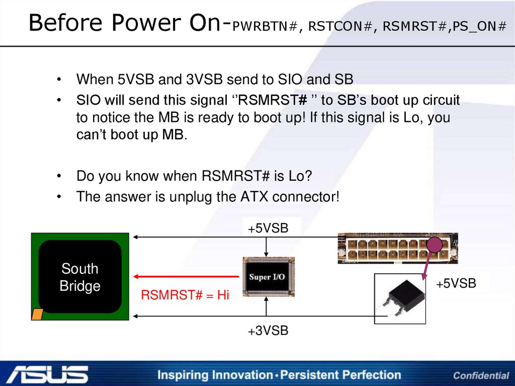
Before Power On-PWRBTN#, RSTCON#, RSMRST#,PS_ON#• When 5VSB and 3VSB send to SIO and SB
• SIO will send this signal ‘’RSMRST# ’’ to SB’s boot up circuit
to notice the MB is ready to boot up! If this signal is Lo, you
can’t boot up MB.
• Do you know when RSMRST# is Lo?
• The answer is unplug the ATX connector!
+5VSB
South
Bridge
+5VSB
RSMRST# = Hi
+3VSB
13.
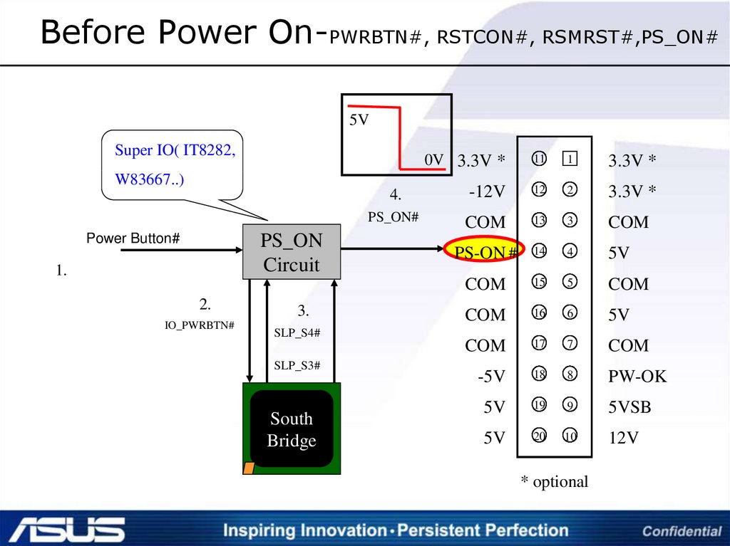
Before Power On-PWRBTN#, RSTCON#, RSMRST#,PS_ON#5V
Super IO( IT8282,
0V 3.3V *
11
1
3.3V *
4.
-12V
12
2
3.3V *
PS_ON#
COM
13
3
COM
PS-ON #
14
4
5V
COM
15
5
COM
COM
16
6
5V
COM
17
7
COM
-5V
18
8
PW-OK
5V
19
9
5VSB
5V
20
10
12V
W83667..)
Power Button#
PS_ON
Circuit
1.
2.
IO_PWRBTN#
3.
SLP_S4#
SLP_S3#
South
Bridge
* optional
14.
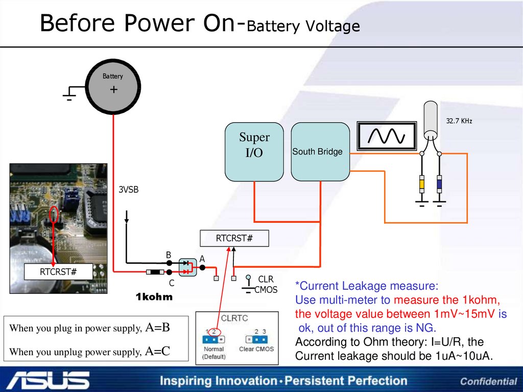
Before Power On-Battery Voltage• Function of Battery Power are:
– CMOS SRAM
– Real Time Clock
15.
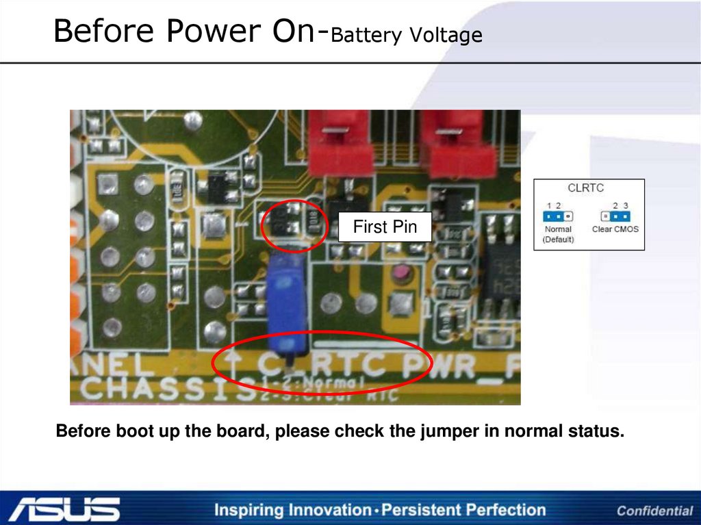
Before Power On-Battery VoltageFirst Pin
Before boot up the board, please check the jumper in normal status.
16.
Before Power On-Battery VoltageBattery
+
32.7 KHz
Super
I/O
South Bridge
3VSB
RTCRST#
B
RTCRST#
C
1kohm
When you plug in power supply, A=B
When you unplug power supply, A=C
A
CLR
CMOS
*Current Leakage measure:
Use multi-meter to measure the 1kohm,
the voltage value between 1mV~15mV is
ok, out of this range is NG.
According to Ohm theory: I=U/R, the
Current leakage should be 1uA~10uA.
17.
Before Power On-Battery VoltageSTART
Use Multi-meter to measure
Current Leakage value
The value is out
of range
ok
NG
Check Battery
Power is 3V
NG
Change Battery,
Measure the C.L.
value is OK.
ok
ok
Check Diode
RB715 is OK
NG
Change diode,
Measure the C.L.
value is OK
ok
ok
Check Vbatt related
Components I/O
ok
Change SB
ok
Finished
NG
Change I/O,
Measure the C.L.
value is OK
ok
18.
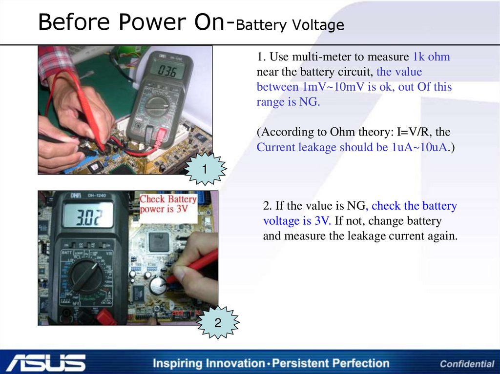
Before Power On-Battery Voltage1. Use multi-meter to measure 1k ohm
near the battery circuit, the value
between 1mV~10mV is ok, out Of this
range is NG.
(According to Ohm theory: I=V/R, the
Current leakage should be 1uA~10uA.)
1
2. If the value is NG, check the battery
voltage is 3V. If not, change battery
and measure the leakage current again.
2
19.
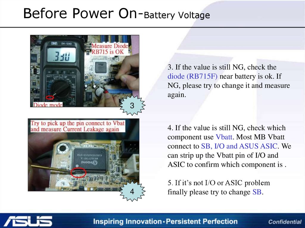
Before Power On-Battery Voltage3. If the value is still NG, check the
diode (RB715F) near battery is ok. If
NG, please try to change it and measure
again.
3
4. If the value is still NG, check which
component use Vbatt. Most MB Vbatt
connect to SB, I/O and ASUS ASIC. We
can strip up the Vbatt pin of I/O and
ASIC to confirm which component is .
4
5. If it’s not I/O or ASIC problem
finally please try to change SB.
20.
AFTER POWER ON VOLTAGE21.
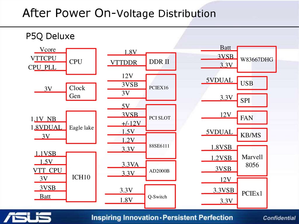
After Power On-Voltage DistributionP5Q Deluxe
Vcore
VTTCPU
CPU_PLL
3V
1.1V_NB
1.8VDUAL
3V
1.1VSB
1.5V
VTT_CPU
3V
3VSB
Batt
1.8V
CPU
Clock
Gen
Eagle lake
VTTDDR
12V
3VSB
3V
5V
3VSB
+/-12V
1.5V
1.2V
3.3V
DDR II
Batt
3VSB W83667DHG
3.3V
5VDUAL
PCIEX16
PCI SLOT
3.3V
SPI
12V
FAN
5VDUAL
88SE6111
ICH10
AD2000B
KB/MS
1.8VSB
1.2VSB
3.3VA
3.3V
USB
3VSB
Marvell
8056
12V
3.3V
1.8V
3.3VSB
Q-Switch
3.3V
PCIEx1
22.
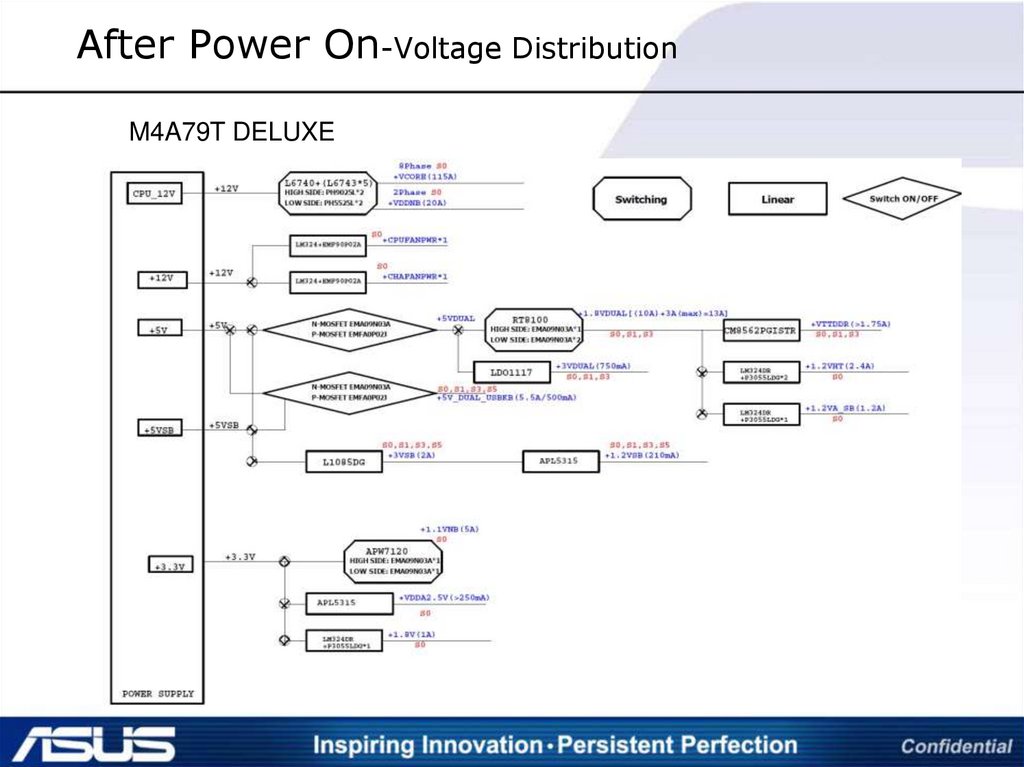
After Power On-Voltage DistributionM4A79T DELUXE
23.
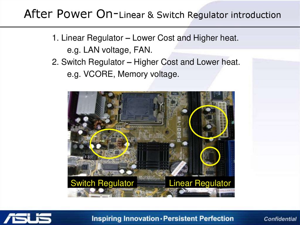
After Power On-Linear & Switch Regulator introduction1. Linear Regulator – Lower Cost and Higher heat.
e.g. LAN voltage, FAN.
2. Switch Regulator – Higher Cost and Lower heat.
e.g. VCORE, Memory voltage.
Switch Regulator
Linear Regulator
24.
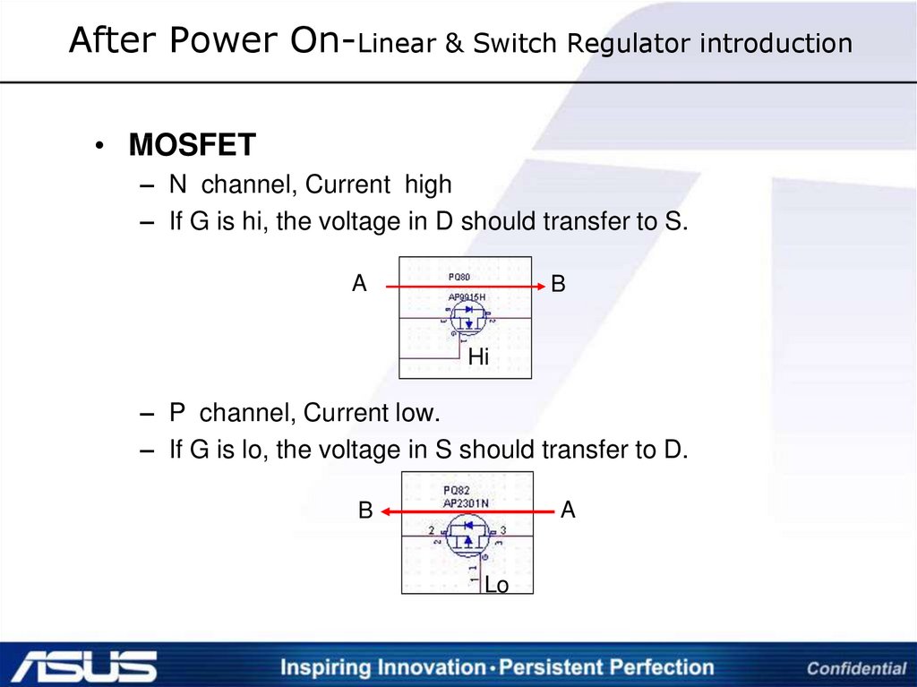
After Power On-Linear & Switch Regulator introduction• MOSFET
– N channel, Current high
– If G is hi, the voltage in D should transfer to S.
A
B
Hi
– P channel, Current low.
– If G is lo, the voltage in S should transfer to D.
A
B
Lo
25.
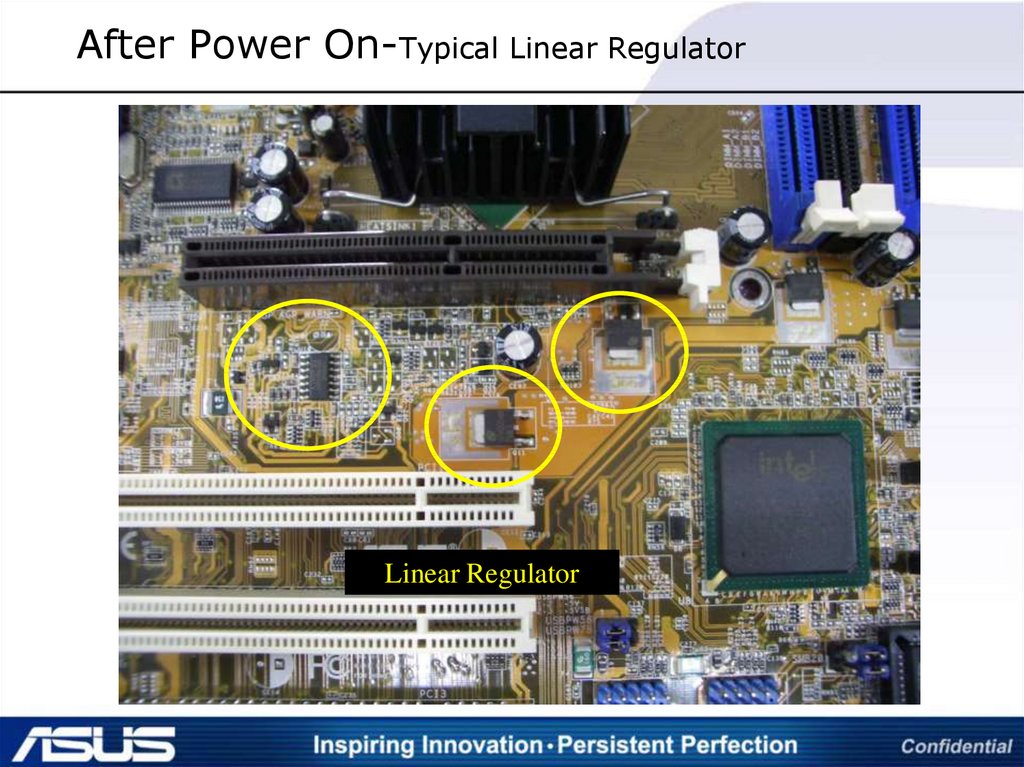
After Power On-Typical Linear RegulatorLinear Regulator
26.
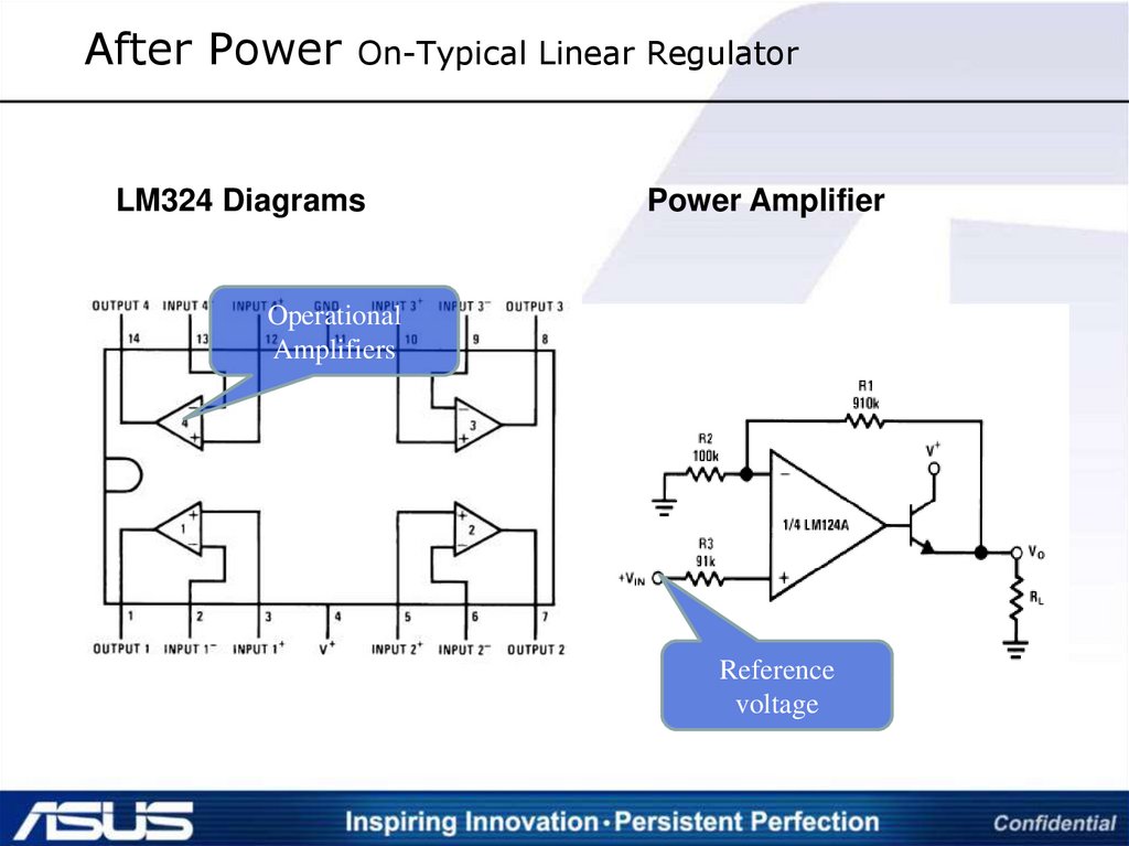
After PowerOn-Typical Linear Regulator
LM324 Diagrams
Power Amplifier
Operational
Amplifiers
Reference
voltage
27.
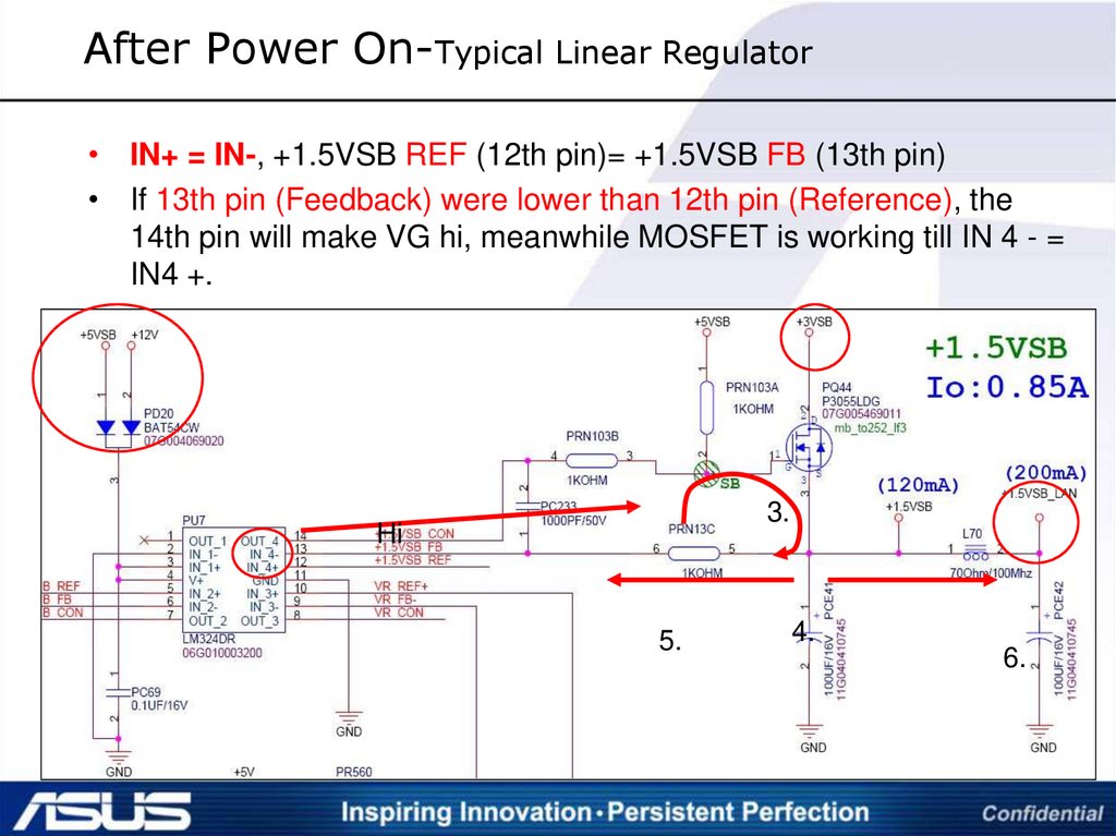
After Power On-Typical Linear Regulator• IN+ = IN-, +1.5VSB REF (12th pin)= +1.5VSB FB (13th pin)
• If 13th pin (Feedback) were lower than 12th pin (Reference), the
14th pin will make VG hi, meanwhile MOSFET is working till IN 4 - =
IN4 +.
1.
Input
Hi
Output
3.
2.
5.
4.
6.
28.
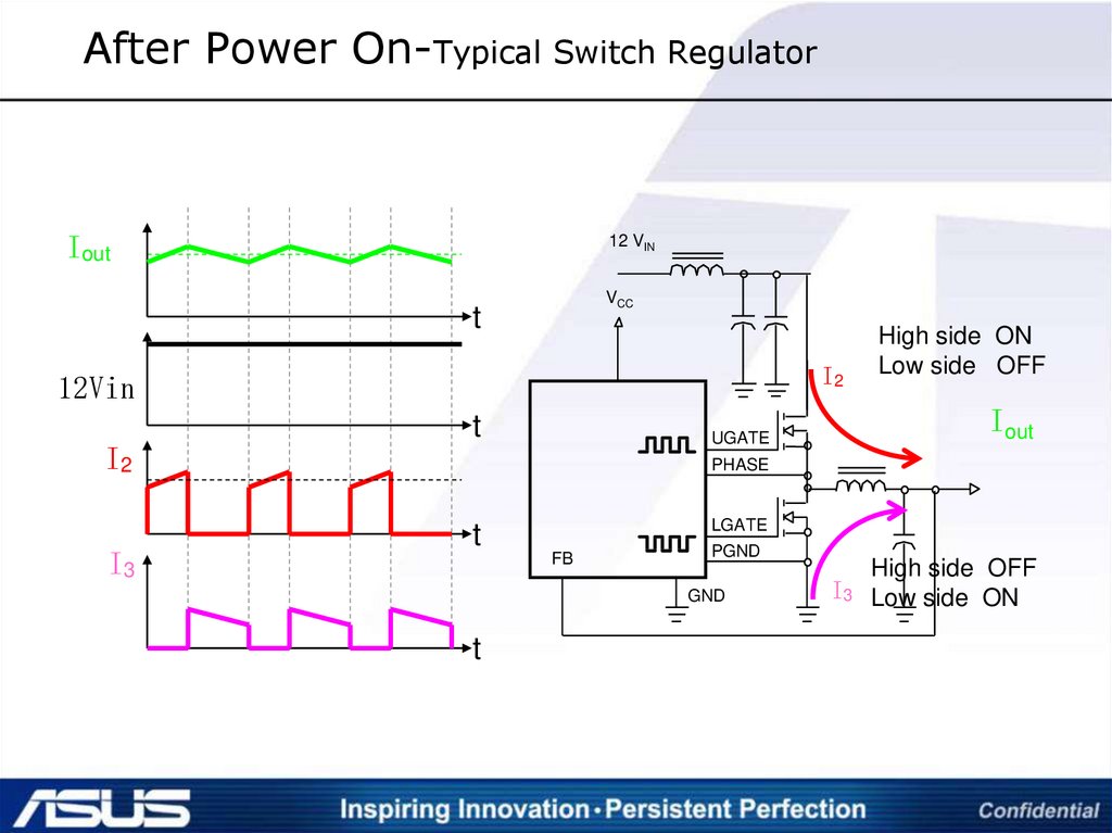
After Power On-Typical Switch RegulatorSwitch Regulator
Switch Regulator
29.
After Power On-Typical Switch RegulatorIout
12 VIN
VCC
t
I2
12Vin
t
UGATE
I2
I3
High side ON
Low side OFF
Iout
PHASE
LGATE
t
FB
PGND
GND
t
High side OFF
I3 Low side ON
30.
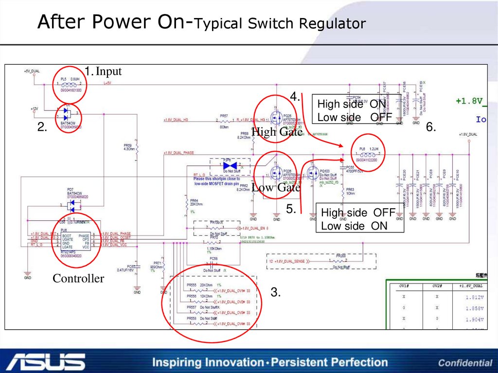
After Power On-Typical Switch Regulator1. Input
4.
2.
High side ON
Low side OFF
High Gate
Low Gate
5.
Controller
3.
High side OFF
Low side ON
6.
31.
VCORE32.
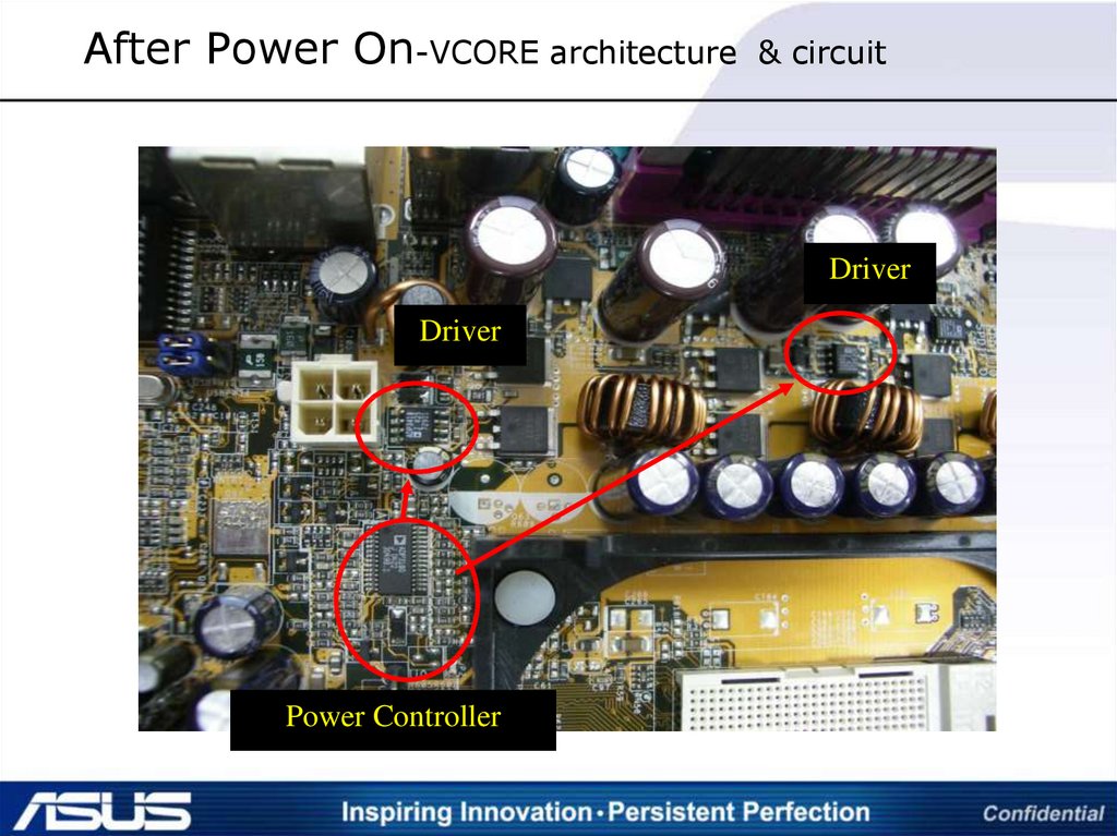
After Power On-VCORE architecture& circuit
Driver
Driver
Power Controller
33.
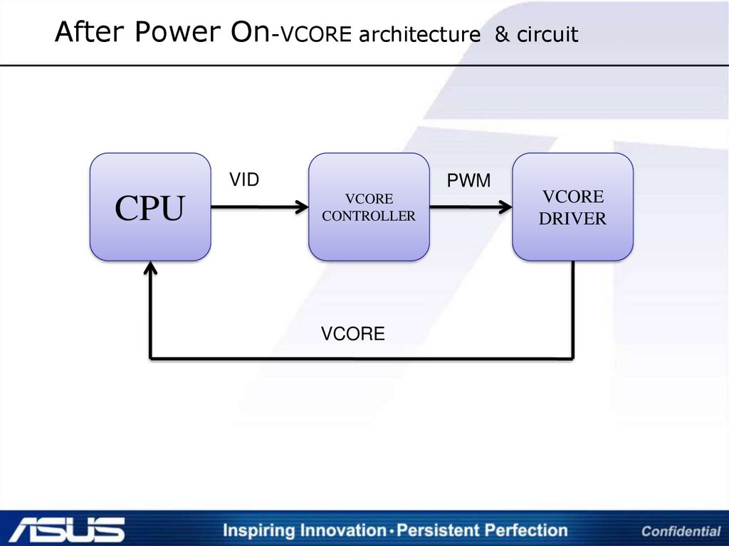
After Power On-VCORE architectureVID
CPU
PWM
VCORE
CONTROLLER
VCORE
& circuit
VCORE
DRIVER
34.
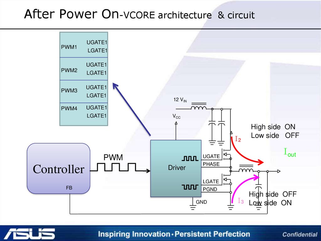
After Power On-VCORE architecturePWM1
& circuit
UGATE1
LGATE1
UGATE1
PWM2
PWM3
LGATE1
UGATE1
LGATE1
PWM4
12 VIN
UGATE1
LGATE1
VCC
I2
PWM
Controller
Iout
UGATE
Driver
High side ON
Low side OFF
PHASE
LGATE
FB
PGND
GND
I3
High side OFF
Low side ON
35.
After Power On-VCORE architecture& circuit
PWM
VCORE Control IC—ADP3180
VID
36.
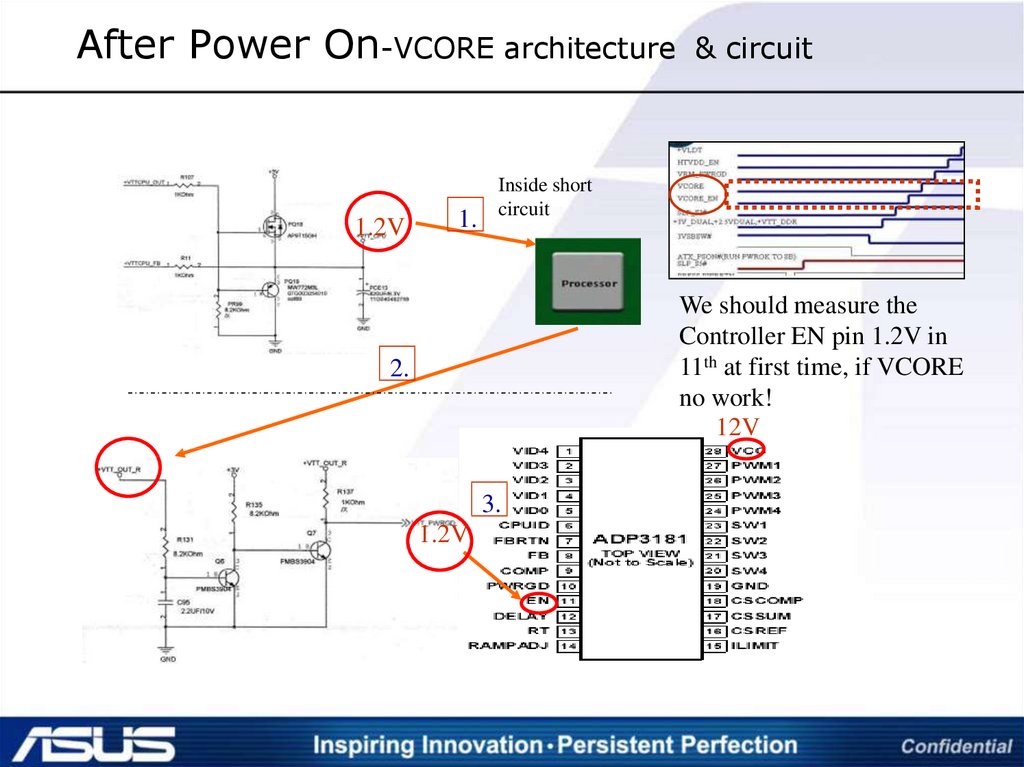
After Power On-VCORE architecture1.2V
1.
& circuit
Inside short
circuit
We should measure the
Controller EN pin 1.2V in
11th at first time, if VCORE
no work!
12V
2.
3.
1.2V
37.
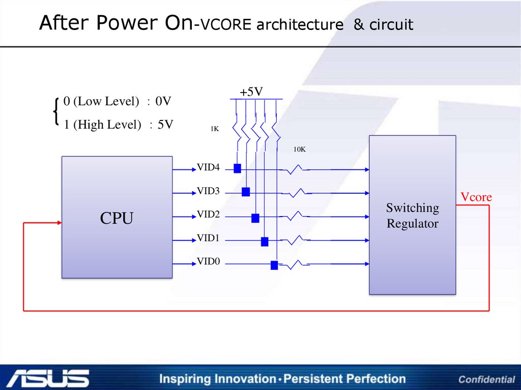
After Power On-VCORE architecture+5V
0 (Low Level) 0V
1 (High Level) 5V
& circuit
1K
10K
VID4
VID3
CPU
VID2
VID1
VID0
Switching
Regulator
Vcore
38.
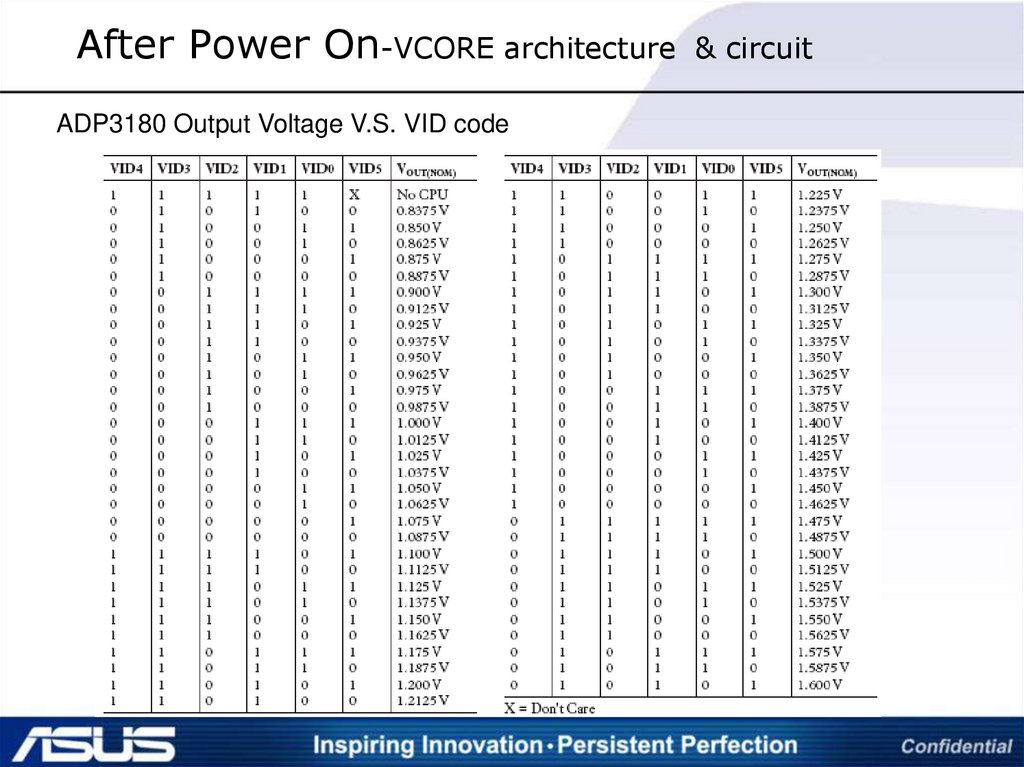
After Power On-VCORE architectureADP3180 Output Voltage V.S. VID code
& circuit
39.
After Power On-VCORE Voltage repair Flow Chart 1START
‧12V Impedance
‧Vcore Impedance
‧12V to Vcore Impedance
No short?
NO
1.Impedance in 12V is
<100
2.Impedance in VCORE is
<50
3.Impedance from 12V to VCORE is
<100
Yes
Boot up
NO
Check Vcore OK?
All wave OK?
Yes
Check
whether
boot after
repairing?
Yes
Other Circuit fail:
Example: PWM IC fail,
RC small component or
soldering fail.
NO
END
Check
Power
Supply work
OK?
NO
Yes
Check PWM
IC EN PIN
1.25V OK?
NO
Other Circuit fail:
Example: Socket fail
1.25VTT_CPU fail
40.
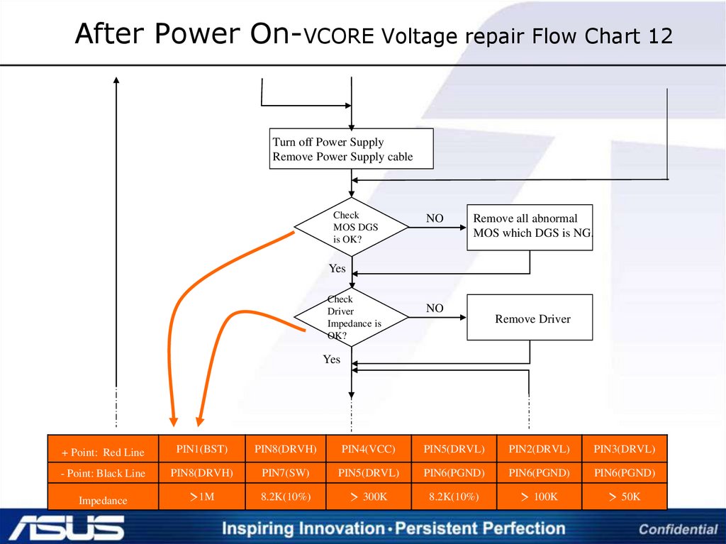
After Power On-VCORE Voltage repair Flow Chart 12Turn off Power Supply
Remove Power Supply cable
Check
MOS DGS
is OK?
NO
Remove all abnormal
MOS which DGS is NG.
Yes
Check
Driver
Impedance is
OK?
NO
Remove Driver
Yes
+ Point: Red Line
PIN1(BST)
PIN8(DRVH)
PIN4(VCC)
PIN5(DRVL)
PIN2(DRVL)
PIN3(DRVL)
- Point: Black Line
PIN8(DRVH)
PIN7(SW)
PIN5(DRVL)
PIN6(PGND)
PIN6(PGND)
PIN6(PGND)
Impedance
>1M
8.2K(10%)
> 300K
8.2K(10%)
> 100K
> 50K
41.
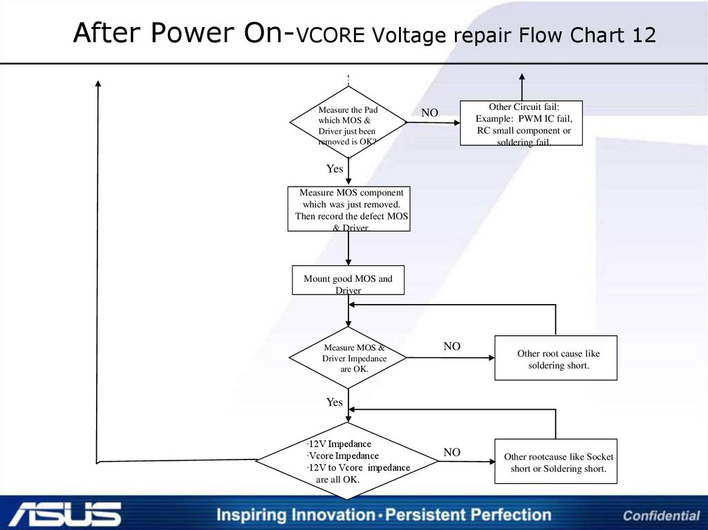
After Power On-VCORE Voltage repair Flow Chart 12Measure the Pad
which MOS &
Driver just been
removed is OK?
Other Circuit fail:
Example: PWM IC fail,
RC small component or
soldering fail.
NO
Yes
Measure MOS component
which was just removed.
Then record the defect MOS
& Driver.
Mount good MOS and
Driver
Measure MOS &
Driver Impedance
are OK.
NO
Other root cause like
soldering short.
Yes
‧12V Impedance
‧Vcore Impedance
‧12V to Vcore impedance
are all OK.
NO
Other rootcause like Socket
short or Soldering short.
42.
After Power On-VCORE Problem Debug Procedure (1)• If no Output
– Check if both 5V and 12V are OK
– Check if POWER MOSFET (both UGATE/ LGATE) are
not short
– Check all VIDs of Power Regulator are not high
– Check EN/FS of Power Regulator is not zero Volt
43.
After Power On-VCORE Problem Debug Procedure (2)• If the output voltage wrong
– Check if VIDs of Power Regulator are wrong setting
– Check if the feedback resistor divider is wrong
– Check if UGATE and LGATE of Power Regulator with
wrong voltage level
– Check if POWER MOSFET failure