Похожие презентации:
Microcontroller Programming. Lecture 2
1.
Microcontroller ProgrammingLecture 2
2.
BRANCH, CALL AND TIME DELAY• SECTION 3.1: BRANCH INSTRUCTIONS AND LOOPING
• SECTION 3.2: CALL INSTRUCTIONS AND STACK
• SECTION 3.3: AVR TIME DELAY AND INSTRUCTION PIPELINE
3.
SECTION 3.1: BRANCH INSTRUCTIONS AND LOOPINGLooping in AVR
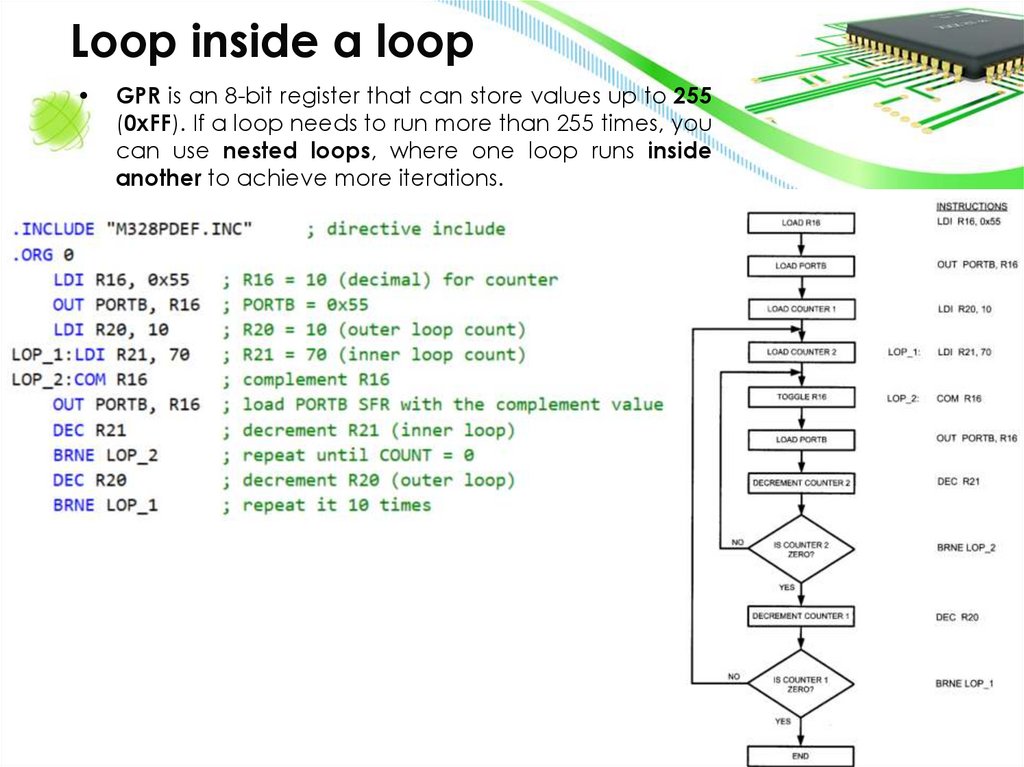
Loop inside a loop
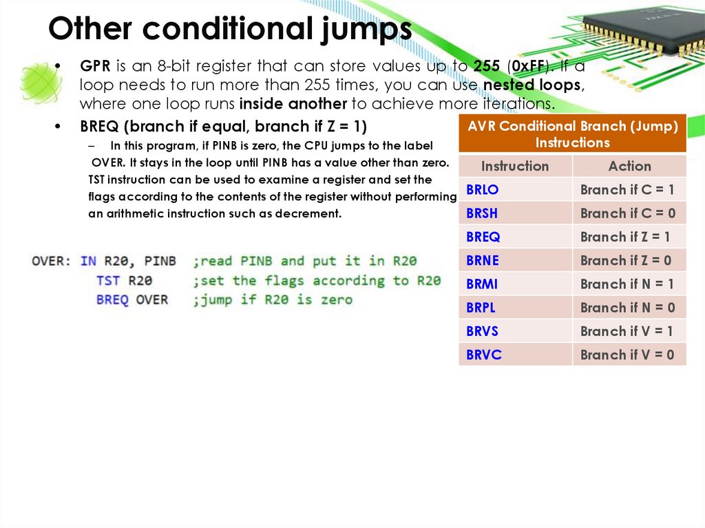
Other conditional jumps
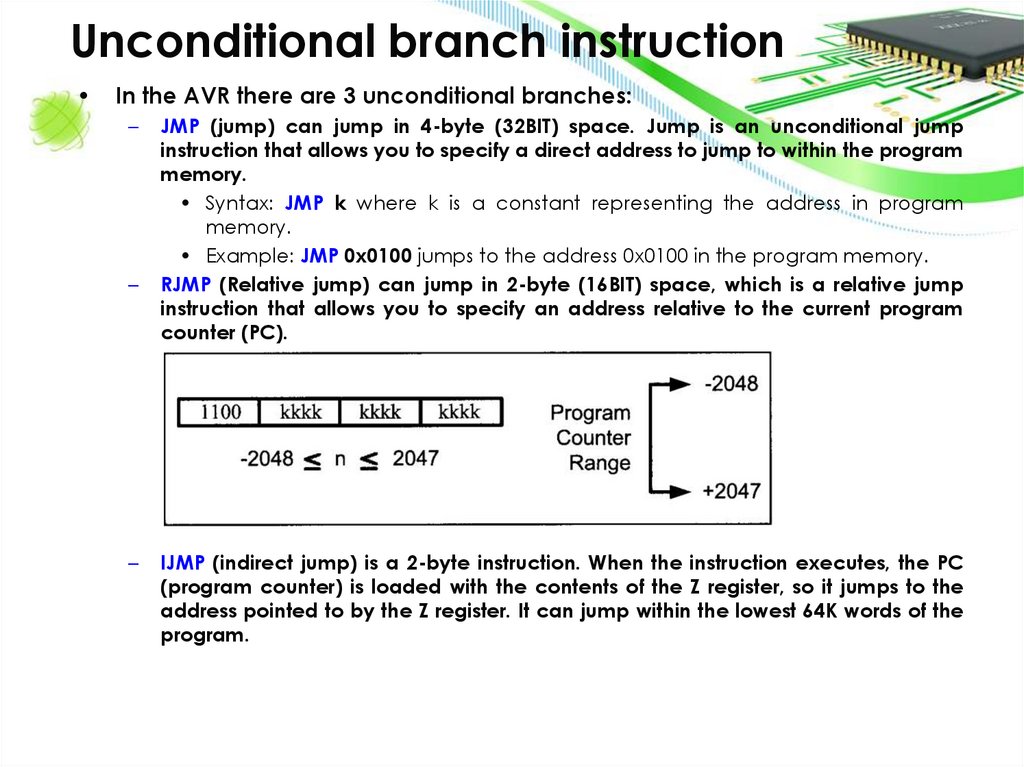
Unconditional branch instruction
4.
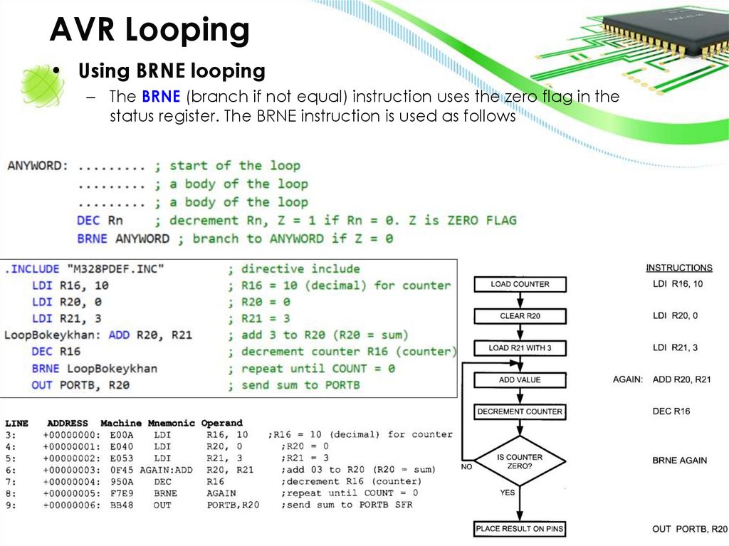
AVR Looping• Using BRNE looping
– The BRNE (branch if not equal) instruction uses the zero flag in the
status register. The BRNE instruction is used as follows
5.
Loop inside a loopGPR is an 8-bit register that can store values up to 255
(0xFF). If a loop needs to run more than 255 times, you
can use nested loops, where one loop runs inside
another to achieve more iterations.
6.
Other conditional jumpsGPR is an 8-bit register that can store values up to 255 (0xFF). If a
loop needs to run more than 255 times, you can use nested loops,
where one loop runs inside another to achieve more iterations.
AVR Conditional Branch (Jump)
BREQ (branch if equal, branch if Z = 1)
Instructions
– In this program, if PINB is zero, the CPU jumps to the label
OVER. It stays in the loop until PINB has a value other than zero.
Instruction
Action
TST instruction can be used to examine a register and set the
BRLO
Branch if C = 1
flags according to the contents of the register without performing
an arithmetic instruction such as decrement.
BRSH
Branch if C = 0
BREQ
Branch if Z = 1
BRNE
Branch if Z = 0
BRMI
Branch if N = 1
BRPL
Branch if N = 0
BRVS
Branch if V = 1
BRVC
Branch if V = 0
7.
Unconditional branch instructionIn the AVR there are 3 unconditional branches:
–
–
–
JMP (jump) can jump in 4-byte (32BIT) space. Jump is an unconditional jump
instruction that allows you to specify a direct address to jump to within the program
memory.
• Syntax: JMP k where k is a constant representing the address in program
memory.
• Example: JMP 0x0100 jumps to the address 0x0100 in the program memory.
RJMP (Relative jump) can jump in 2-byte (16BIT) space, which is a relative jump
instruction that allows you to specify an address relative to the current program
counter (PC).
IJMP (indirect jump) is a 2-byte instruction. When the instruction executes, the PC
(program counter) is loaded with the contents of the Z register, so it jumps to the
address pointed to by the Z register. It can jump within the lowest 64K words of the
program.
8.
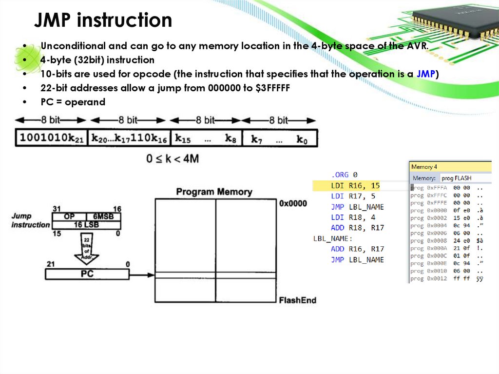
JMP instructionUnconditional and can go to any memory location in the 4-byte space of the AVR.
4-byte (32bit) instruction
10-bits are used for opcode (the instruction that specifies that the operation is a JMP)
22-bit addresses allow a jump from 000000 to $3FFFFF
PC = operand
9.
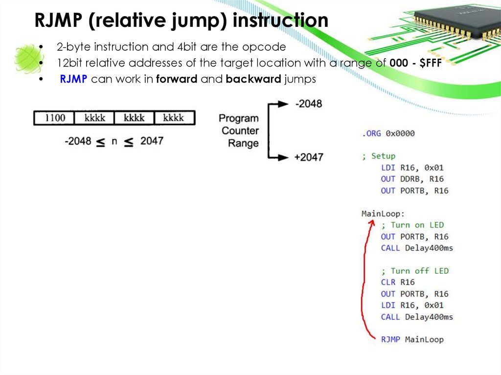
RJMP (relative jump) instruction2-byte instruction and 4bit are the opcode
12bit relative addresses of the target location with a range of 000 - $FFF
RJMP can work in forward and backward jumps
10.
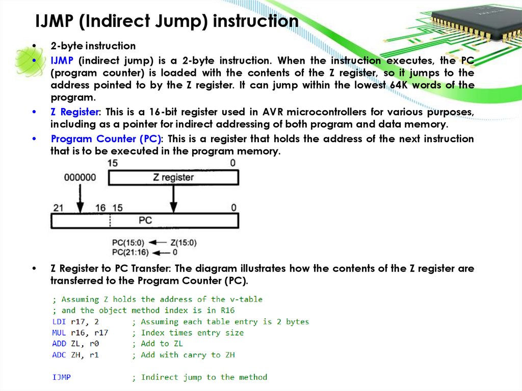
IJMP (Indirect Jump) instruction2-byte instruction
IJMP (indirect jump) is a 2-byte instruction. When the instruction executes, the PC
(program counter) is loaded with the contents of the Z register, so it jumps to the
address pointed to by the Z register. It can jump within the lowest 64K words of the
program.
Z Register: This is a 16-bit register used in AVR microcontrollers for various purposes,
including as a pointer for indirect addressing of both program and data memory.
Program Counter (PC): This is a register that holds the address of the next instruction
that is to be executed in the program memory.
Z Register to PC Transfer: The diagram illustrates how the contents of the Z register are
transferred to the Program Counter (PC).
11.
SECTION 3.2: CALL INSTRUCTIONS AND STACK• CALL
–
–
–
–
–
–
–
–
–
Stack and stack pointer in AVR
How stacks are accessed in the AVR
Pushing onto the stack
Popping from the stack
Initializing the stack pointer
CALL instruction and the role of the stack
RET instruction and the role of the stack
The upper limit of the stack
Calling many subroutines from the main program
• RCALL (relative call)
12.
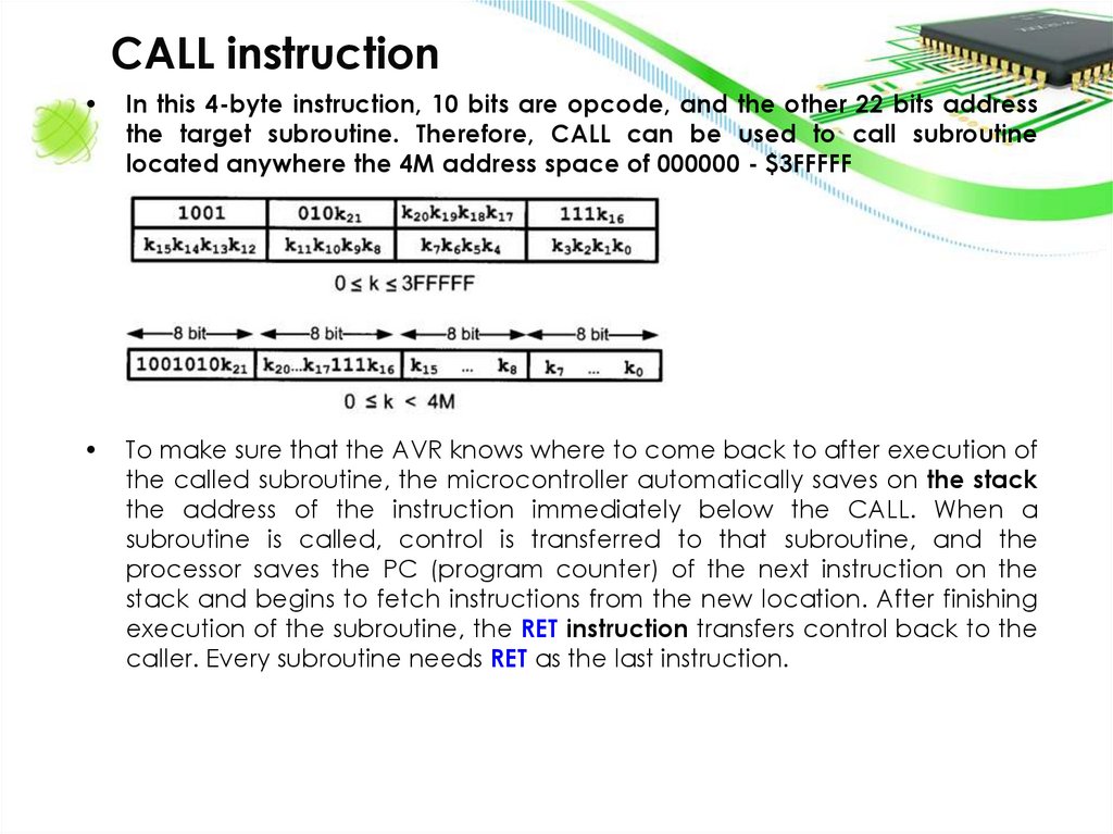
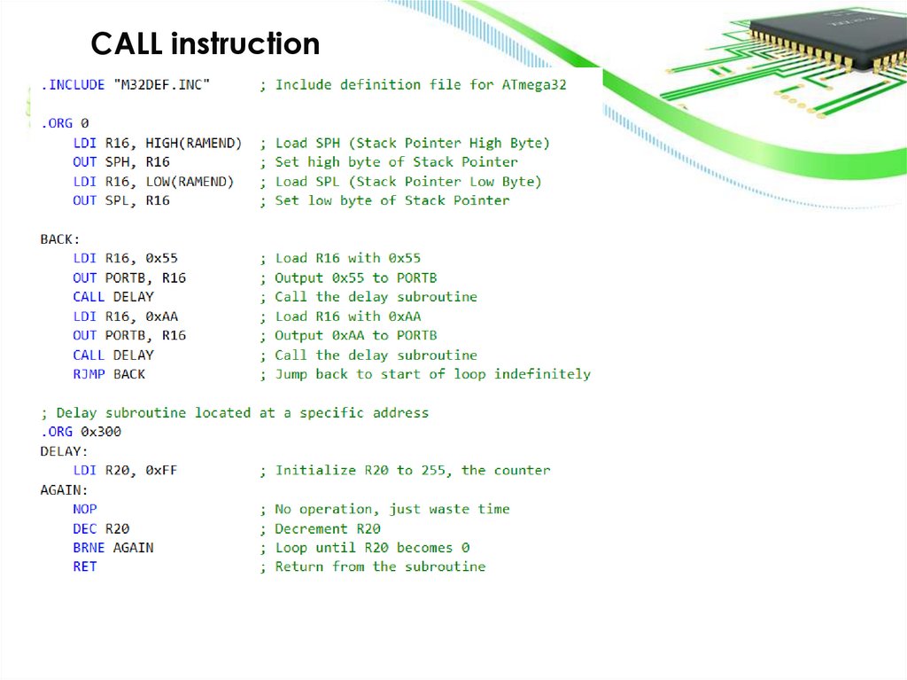
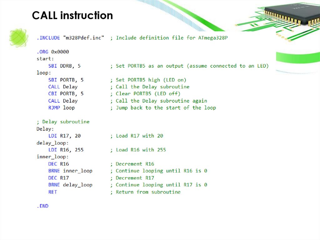
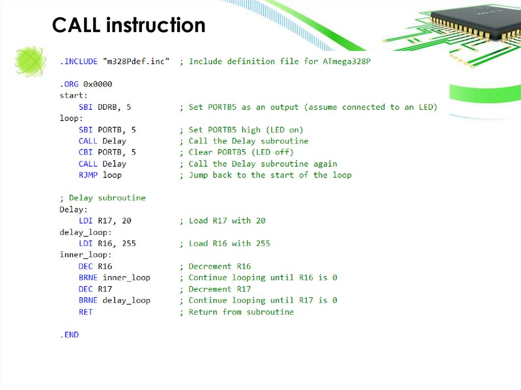
CALL instructionIn this 4-byte instruction, 10 bits are opcode, and the other 22 bits address
the target subroutine. Therefore, CALL can be used to call subroutine
located anywhere the 4M address space of 000000 - $3FFFFF
To make sure that the AVR knows where to come back to after execution of
the called subroutine, the microcontroller automatically saves on the stack
the address of the instruction immediately below the CALL. When a
subroutine is called, control is transferred to that subroutine, and the
processor saves the PC (program counter) of the next instruction on the
stack and begins to fetch instructions from the new location. After finishing
execution of the subroutine, the RET instruction transfers control back to the
caller. Every subroutine needs RET as the last instruction.
13.
CALL instruction14.
CALL instruction15.
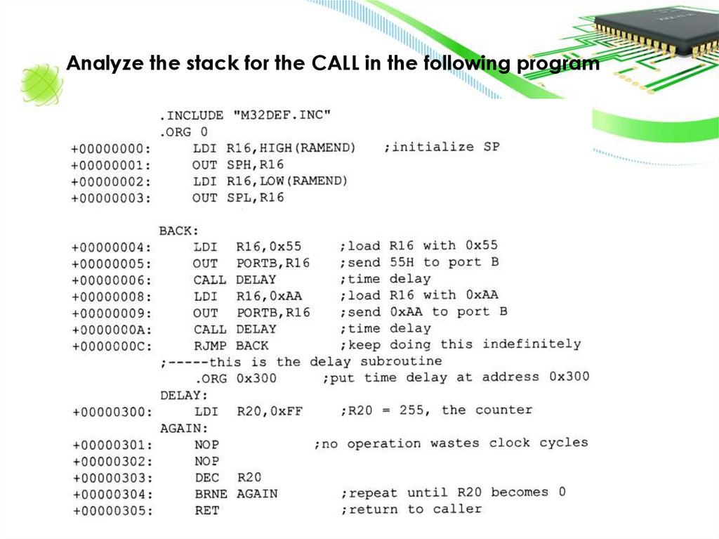
Analyze the stack for the CALL in the following program16.
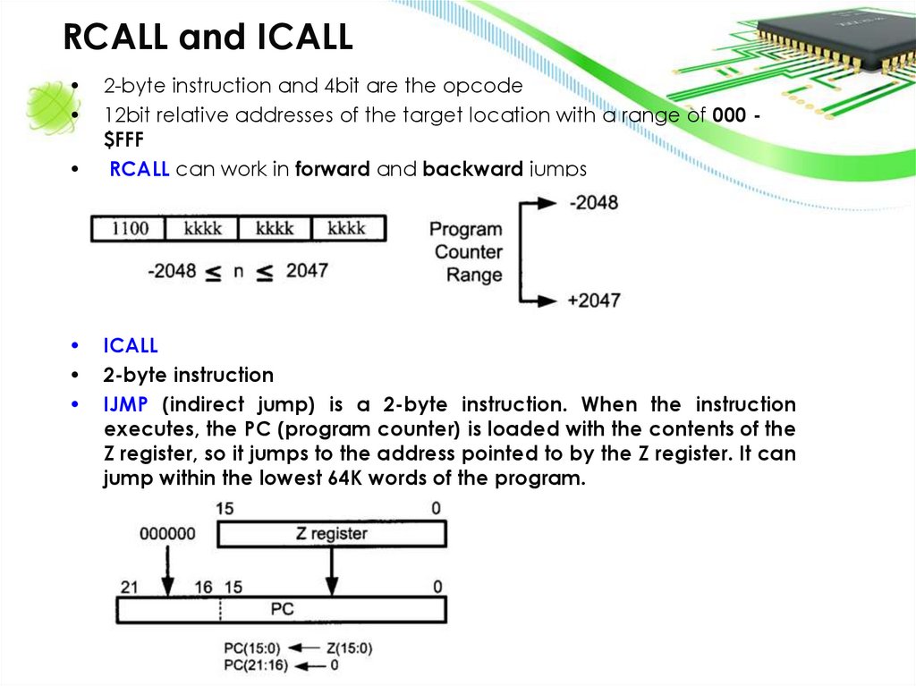
RCALL and ICALL2-byte instruction and 4bit are the opcode
12bit relative addresses of the target location with a range of 000 $FFF
RCALL can work in forward and backward jumps
ICALL
2-byte instruction
IJMP (indirect jump) is a 2-byte instruction. When the instruction
executes, the PC (program counter) is loaded with the contents of the
Z register, so it jumps to the address pointed to by the Z register. It can
jump within the lowest 64K words of the program.
17.
SECTION 3.3: AVR TIME DELAY AND INSTRUCTION PIPELINEDelay calculation for the AVR
Pipelining
AVR multistage execution pipeline
Instruction cycle time for the AVR
Branch penalty
Delay calculation for AVR
Loop inside a loop delay
18.
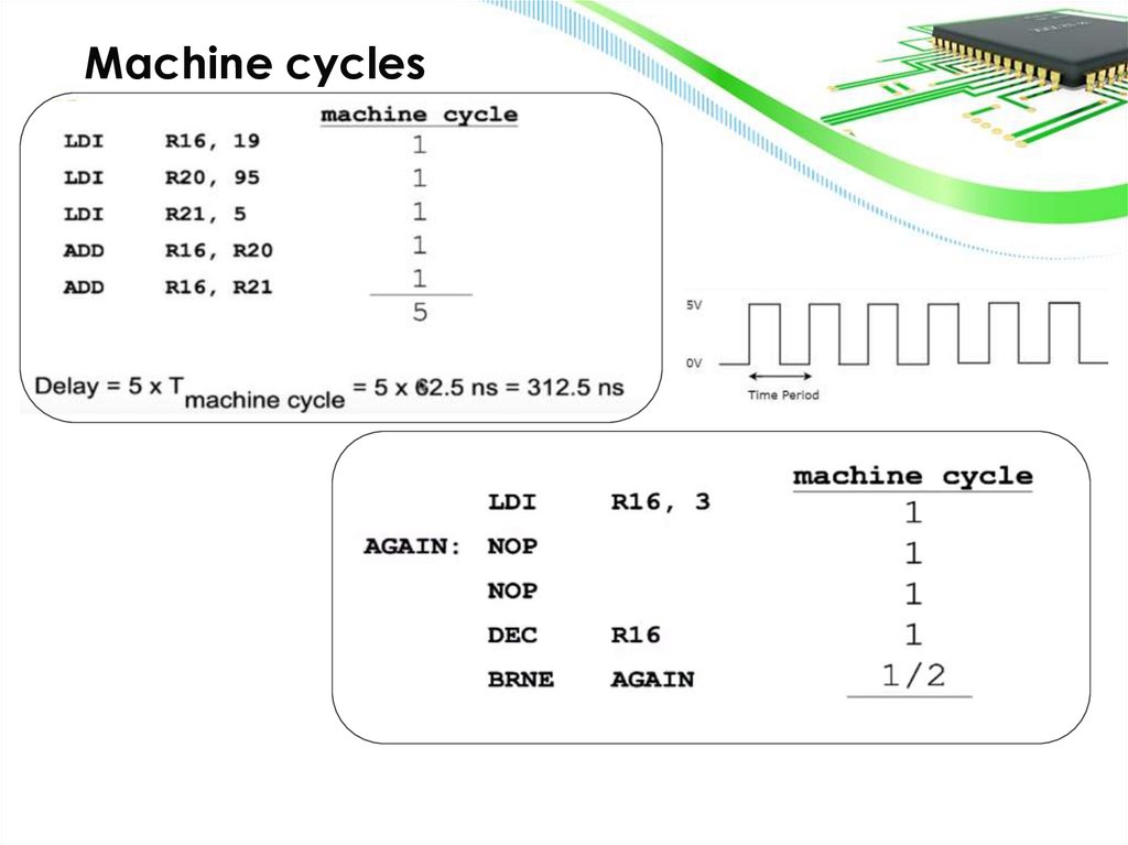
Machine cycles19.
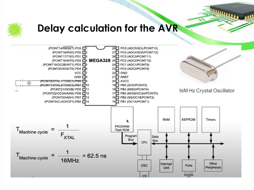
Delay calculation for the AVR20.
CALL instruction21.
AVR I/O PORT PROGRAMMING• SECTION 4.1: I/O PORT PROGRAMMING IN AVR
• SECTION 4.2: I/O BIT MANIPULATION PROGRAMMING
22.
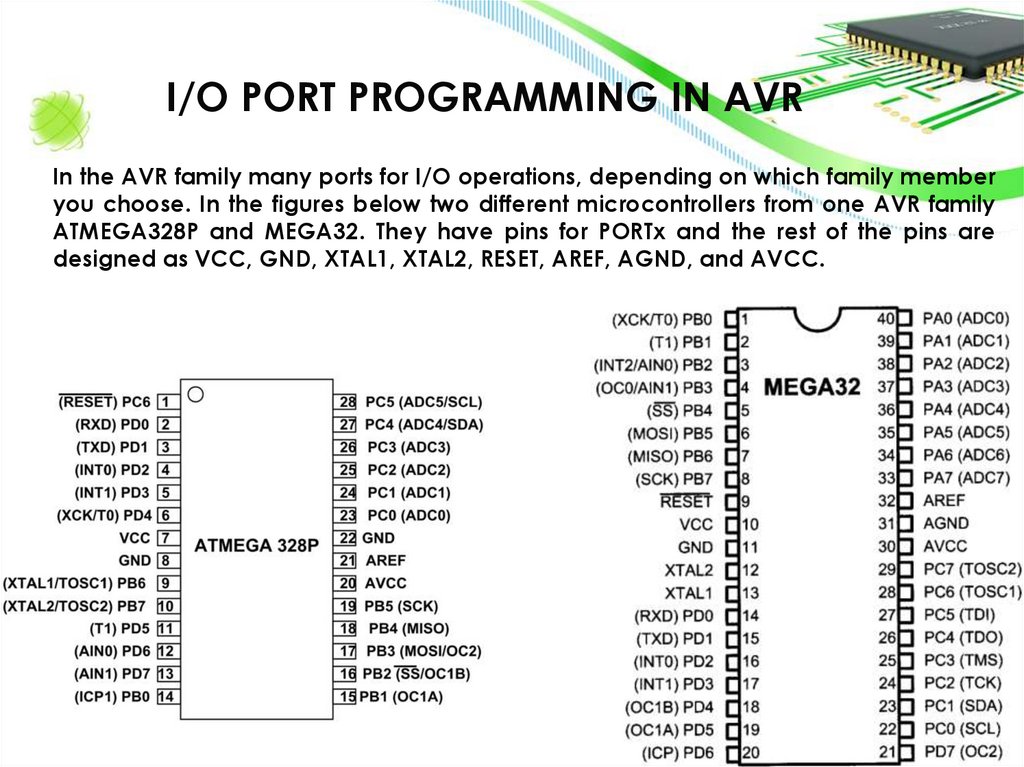
I/O PORT PROGRAMMING IN AVRIn the AVR family many ports for I/O operations, depending on which family member
you choose. In the figures below two different microcontrollers from one AVR family
ATMEGA328P and MEGA32. They have pins for PORTx and the rest of the pins are
designed as VCC, GND, XTAL1, XTAL2, RESET, AREF, AGND, and AVCC.
23.
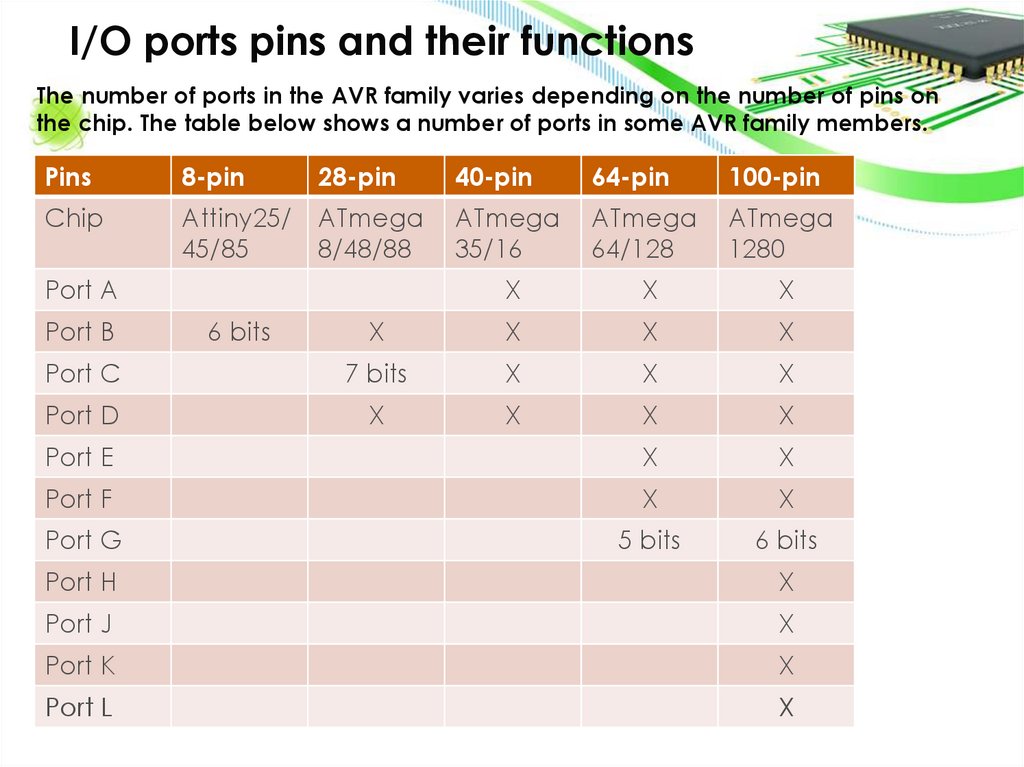
I/O ports pins and their functionsThe number of ports in the AVR family varies depending on the number of pins on
the chip. The table below shows a number of ports in some AVR family members.
Pins
8-pin
28-pin
40-pin
64-pin
100-pin
Chip
Attiny25/
45/85
ATmega
8/48/88
ATmega
35/16
ATmega
64/128
ATmega
1280
X
X
X
X
X
X
X
Port C
7 bits
X
X
X
Port D
X
X
X
X
Port E
X
X
Port F
X
X
Port G
5 bits
6 bits
Port A
Port B
6 bits
Port H
X
Port J
X
Port K
X
Port L
X
24.
ATmega328P PinoutPINs of each port is used not only for I/O and each port has some other
functions such as ADC, timer, interrupts, and serial communication pins.
25.
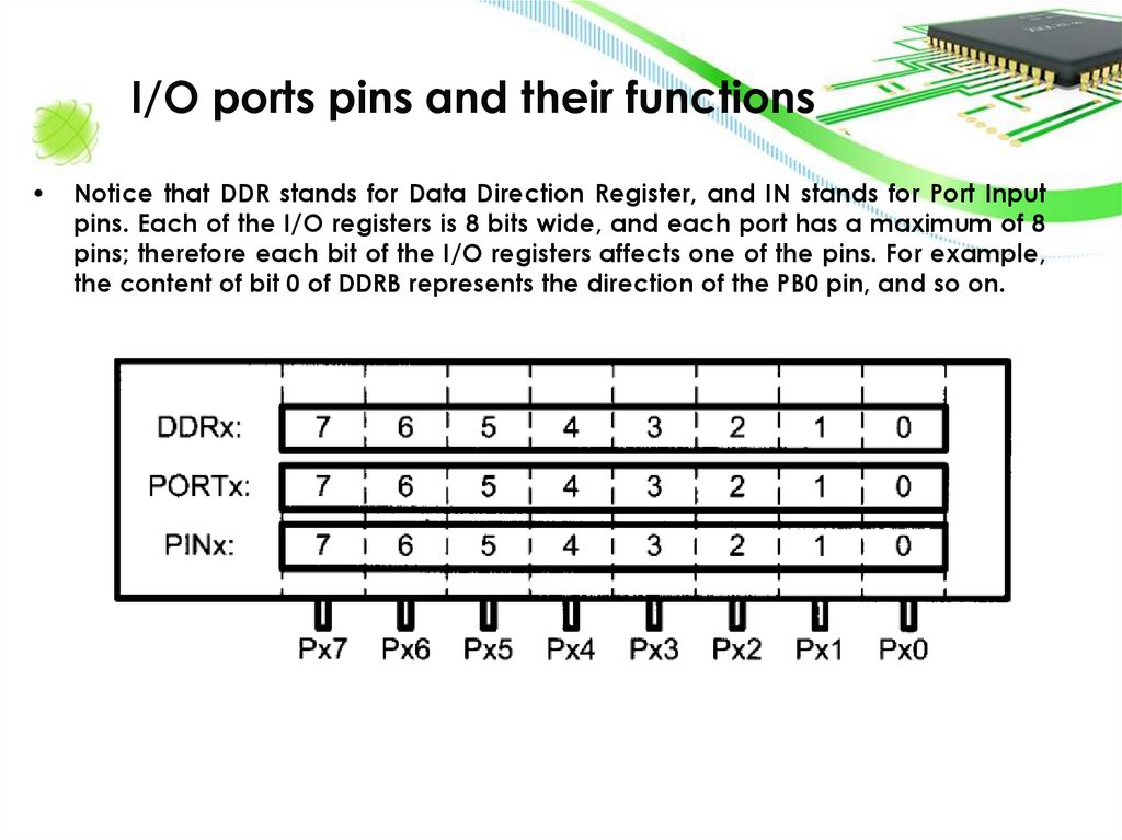
I/O ports pins and their functionsNotice that DDR stands for Data Direction Register, and IN stands for Port Input
pins. Each of the I/O registers is 8 bits wide, and each port has a maximum of 8
pins; therefore each bit of the I/O registers affects one of the pins. For example,
the content of bit 0 of DDRB represents the direction of the PB0 pin, and so on.
26.
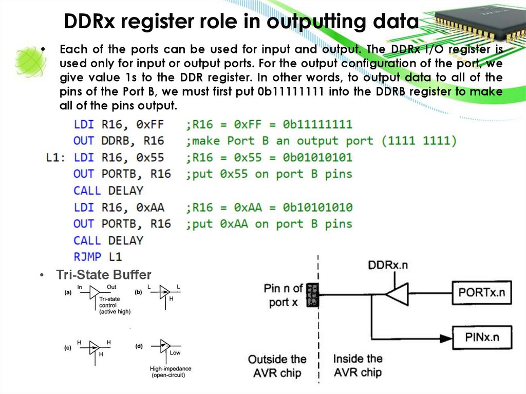
DDRx register role in outputting dataEach of the ports can be used for input and output. The DDRx I/O register is
used only for input or output ports. For the output configuration of the port, we
give value 1s to the DDR register. In other words, to output data to all of the
pins of the Port B, we must first put 0b11111111 into the DDRB register to make
all of the pins output.
• Tri-State Buffer
27.
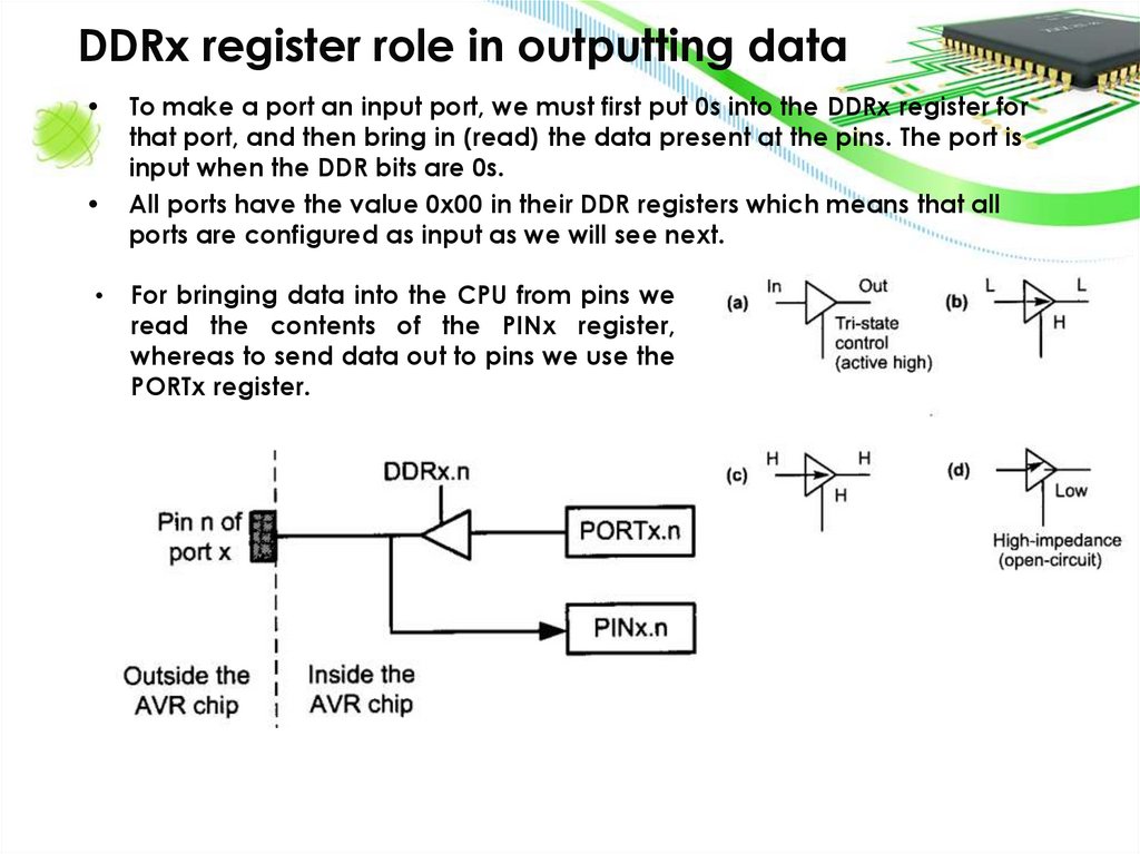
DDRx register role in outputting dataTo make a port an input port, we must first put 0s into the DDRx register for
that port, and then bring in (read) the data present at the pins. The port is
input when the DDR bits are 0s.
All ports have the value 0x00 in their DDR registers which means that all
ports are configured as input as we will see next.
For bringing data into the CPU from pins we
read the contents of the PINx register,
whereas to send data out to pins we use the
PORTx register.
28.
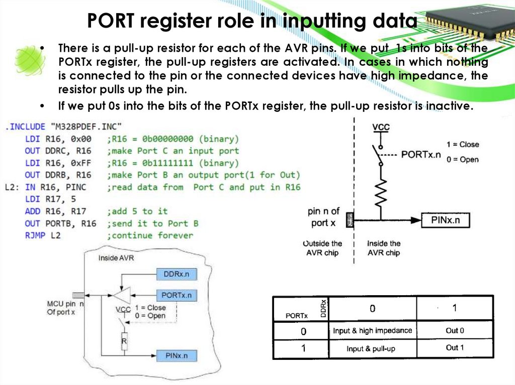
PORT register role in inputting dataThere is a pull-up resistor for each of the AVR pins. If we put 1s into bits of the
PORTx register, the pull-up registers are activated. In cases in which nothing
is connected to the pin or the connected devices have high impedance, the
resistor pulls up the pin.
If we put 0s into the bits of the PORTx register, the pull-up resistor is inactive.
29.
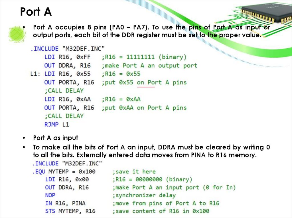
Port APort A occupies 8 pins (PA0 – PA7). To use the pins of Port A as input or
output ports, each bit of the DDR register must be set to the proper value.
Port A as input
To make all the bits of Port A an input, DDRA must be cleared by writing 0
to all the bits. Externally entered data moves from PINA to R16 memory.
30.
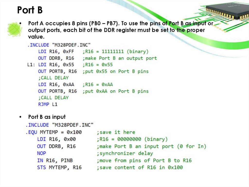
Port BPort A occupies 8 pins (PB0 – PB7). To use the pins of Port B as input or
output ports, each bit of the DDR register must be set to the proper
value.
Port B as input
31.
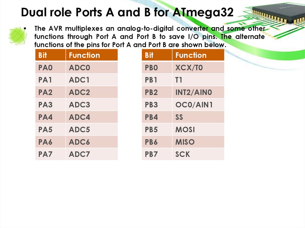
Dual role Ports A and B for ATmega32The AVR multiplexes an analog-to-digital converter and some other
functions through Port A and Port B to save I/O pins. The alternate
functions of the pins for Port A and Port B are shown below.
Bit
Function
Bit
Function
PA0
ADC0
PB0
XCX/T0
PA1
ADC1
PB1
T1
PA2
ADC2
PB2
INT2/AIN0
PA3
ADC3
PB3
OC0/AIN1
PA4
ADC4
PB4
SS
PA5
ADC5
PB5
MOSI
PA6
ADC6
PB6
MISO
PA7
ADC7
PB7
SCK
32.
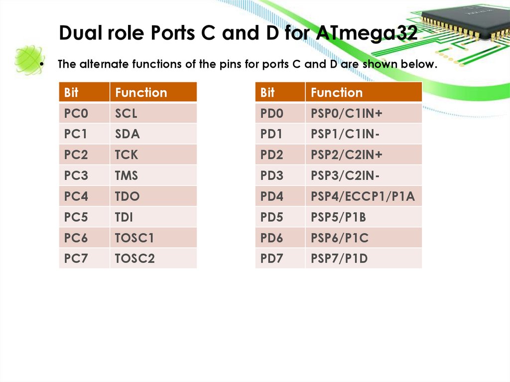
Dual role Ports C and D for ATmega32The alternate functions of the pins for ports C and D are shown below.
Bit
Function
Bit
Function
PC0
SCL
PD0
PSP0/C1IN+
PC1
SDA
PD1
PSP1/C1IN-
PC2
TCK
PD2
PSP2/C2IN+
PC3
TMS
PD3
PSP3/C2IN-
PC4
TDO
PD4
PSP4/ECCP1/P1A
PC5
TDI
PD5
PSP5/P1B
PC6
TOSC1
PD6
PSP6/P1C
PC7
TOSC2
PD7
PSP7/P1D
33.
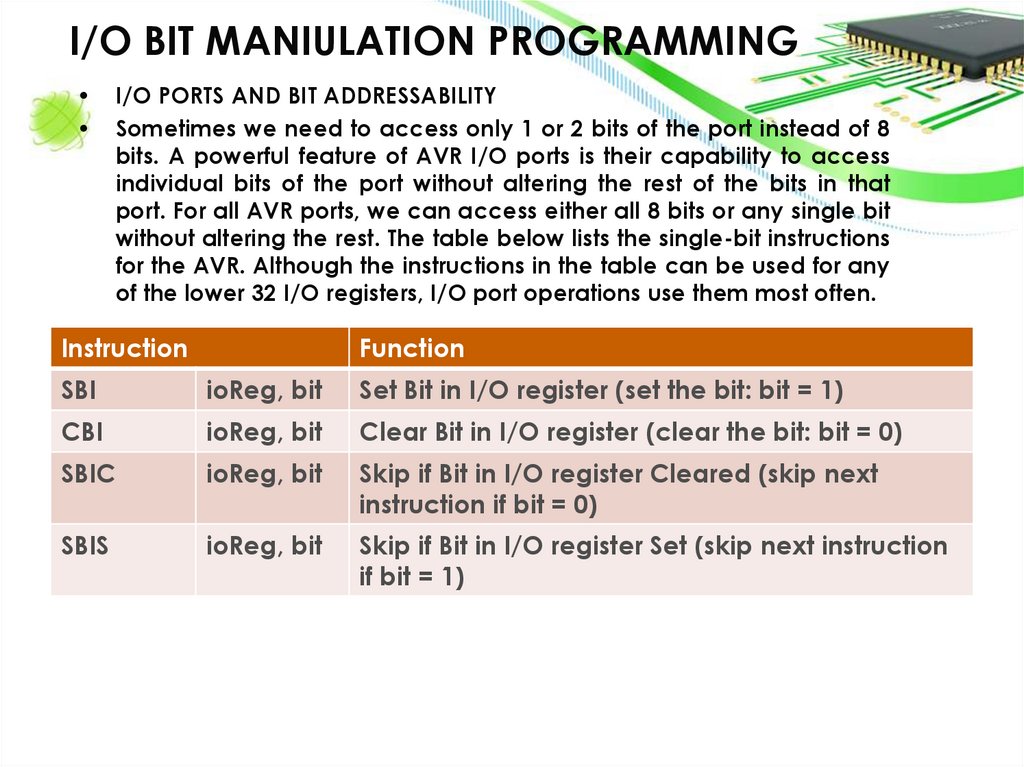
I/O BIT MANIULATION PROGRAMMINGI/O PORTS AND BIT ADDRESSABILITY
Sometimes we need to access only 1 or 2 bits of the port instead of 8
bits. A powerful feature of AVR I/O ports is their capability to access
individual bits of the port without altering the rest of the bits in that
port. For all AVR ports, we can access either all 8 bits or any single bit
without altering the rest. The table below lists the single-bit instructions
for the AVR. Although the instructions in the table can be used for any
of the lower 32 I/O registers, I/O port operations use them most often.
Instruction
Function
SBI
ioReg, bit
Set Bit in I/O register (set the bit: bit = 1)
CBI
ioReg, bit
Clear Bit in I/O register (clear the bit: bit = 0)
SBIC
ioReg, bit
Skip if Bit in I/O register Cleared (skip next
instruction if bit = 0)
SBIS
ioReg, bit
Skip if Bit in I/O register Set (skip next instruction
if bit = 1)
34.
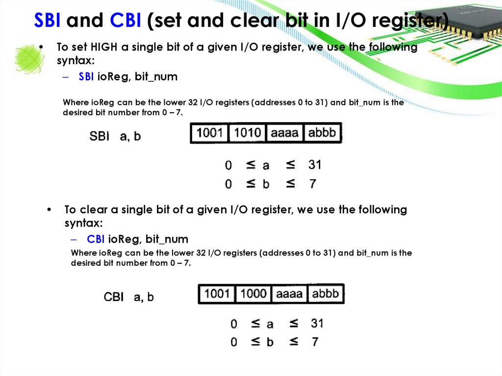
SBI and CBI (set and clear bit in I/O register)To set HIGH a single bit of a given I/O register, we use the following
syntax:
– SBI ioReg, bit_num
Where ioReg can be the lower 32 I/O registers (addresses 0 to 31) and bit_num is the
desired bit number from 0 – 7.
To clear a single bit of a given I/O register, we use the following
syntax:
– CBI ioReg, bit_num
Where ioReg can be the lower 32 I/O registers (addresses 0 to 31) and bit_num is the
desired bit number from 0 – 7.
35.
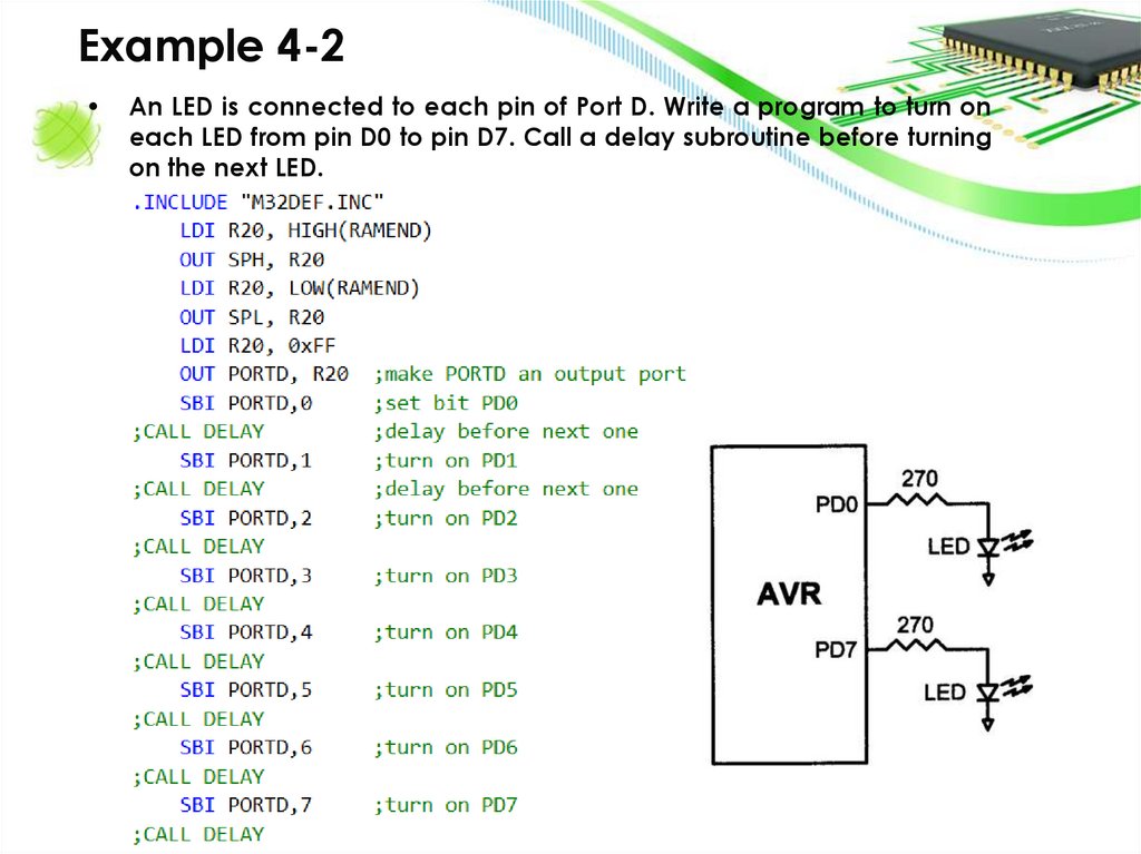
Example 4-2An LED is connected to each pin of Port D. Write a program to turn on
each LED from pin D0 to pin D7. Call a delay subroutine before turning
on the next LED.
36.
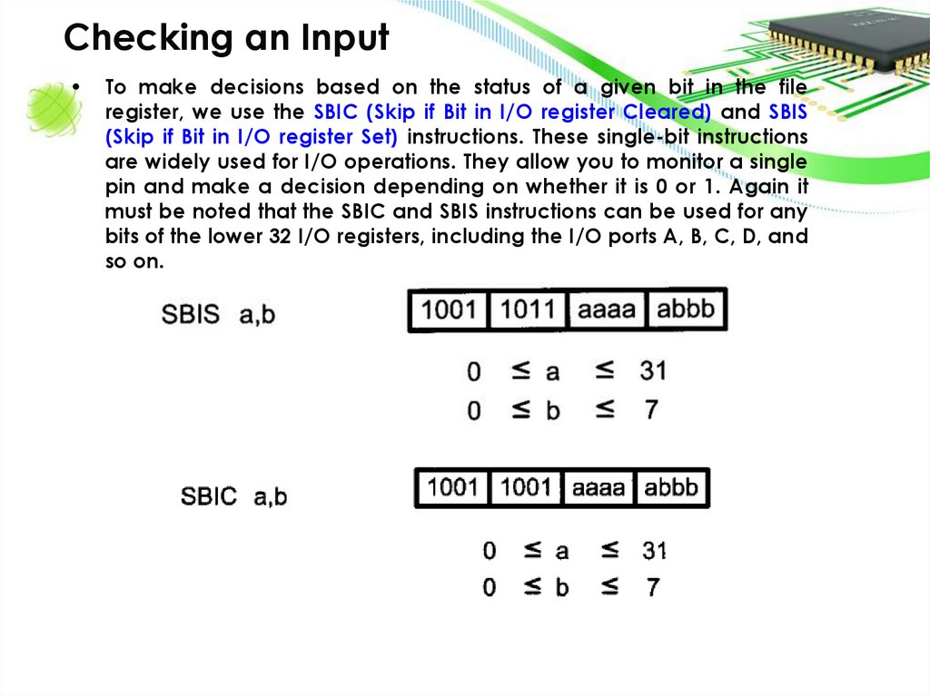
Checking an InputTo make decisions based on the status of a given bit in the file
register, we use the SBIC (Skip if Bit in I/O register Cleared) and SBIS
(Skip if Bit in I/O register Set) instructions. These single-bit instructions
are widely used for I/O operations. They allow you to monitor a single
pin and make a decision depending on whether it is 0 or 1. Again it
must be noted that the SBIC and SBIS instructions can be used for any
bits of the lower 32 I/O registers, including the I/O ports A, B, C, D, and
so on.
37.
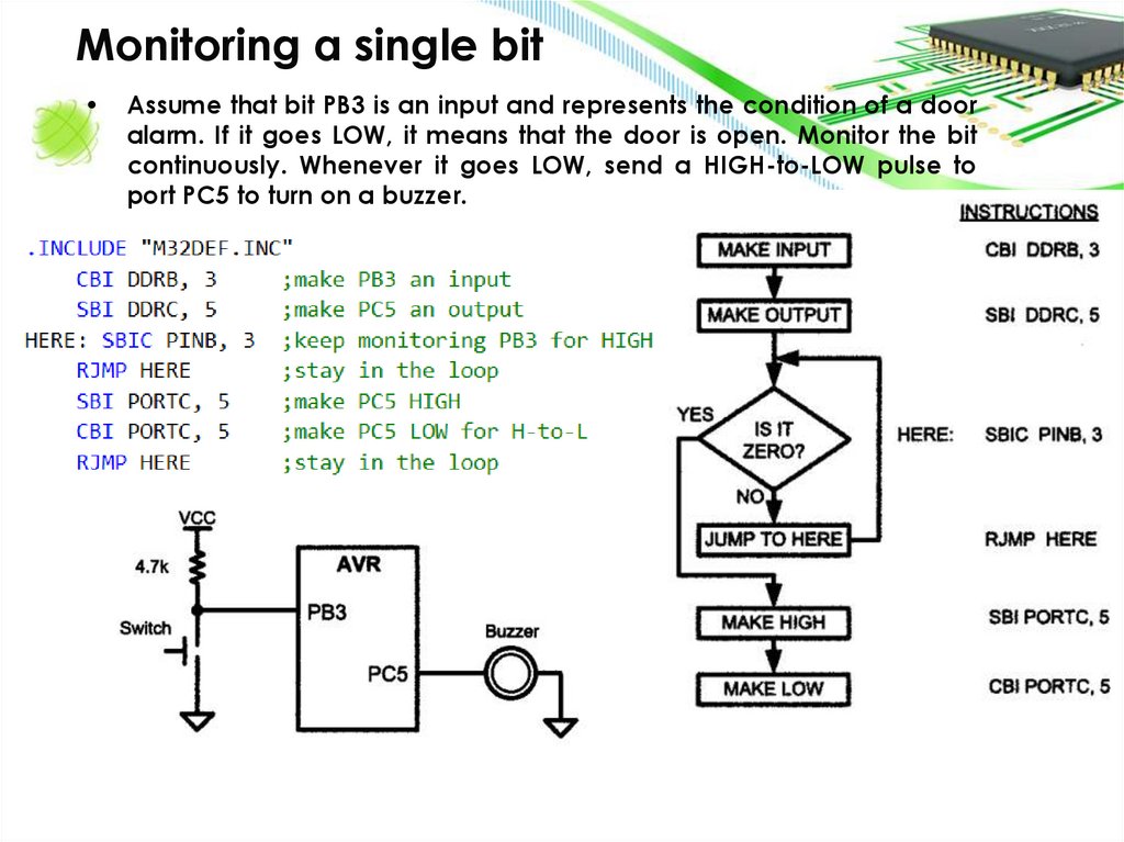
Monitoring a single bitAssume that bit PB3 is an input and represents the condition of a door
alarm. If it goes LOW, it means that the door is open. Monitor the bit
continuously. Whenever it goes LOW, send a HIGH-to-LOW pulse to
port PC5 to turn on a buzzer.
38.
SDSDS
39.
Thanks for your attention!• Thanks for your attention!



 Электроника


