


 Информатика
Похожие презентации:


")


Introduction to Digital Systems. Combinational Circuits. Digital Integrated Circuits. Lecture 1
1.
LECTURE 12.
Introduction to Digital Systems. CombinationalCircuits. Digital Integrated Circuits.
Lecture 1
Dana Utebayeva
3.
Outline• Deriving logical expressions
• Basic concepts
• Simple gates
• Completeness
• Logic functions
• Expressing logic functions
• Equivalence
• Boolean algebra
• Boolean identities
• Logical equivalence
• Logic Circuit Design Process
• Sum-of-products form
• Product-of-sums form
• Simplifying logical
expressions
• Algebraic manipulation
• Karnaugh map method
• Quine-McCluskey method
• Generalized gates
• Multiple outputs
• Implementation using other
gates (NAND and XOR)
4.
Introduction• Hardware consists of a few simple building blocks
• These are called logic gates
• AND, OR, NOT, …
• NAND, NOR, XOR, …
• Logic gates are built using transistors
• NOT gate can be implemented by a single transistor
• AND gate requires 3 transistors
• Transistors are the fundamental devices
• Pentium consists of 3 million transistors
• Compaq Alpha consists of 9 million transistors
• Now we can build chips with more than 100 million transistors
5.
Basic Concepts• Simple gates
• AND
• OR
• NOT
• Functionality can be expressed by a
truth table
• A truth table lists output for each
possible input combination
• Other methods
• Logic expressions
• Logic diagrams
6.
Basic Concepts (cont’d)• Additional useful gates
• NAND
• NOR
• XOR
• NAND = AND + NOT
• NOR = OR + NOT
• XOR implements exclusive-OR
function
• NAND and NOR gates require only 2
transistors
• AND and OR need 3 transistors!
7.
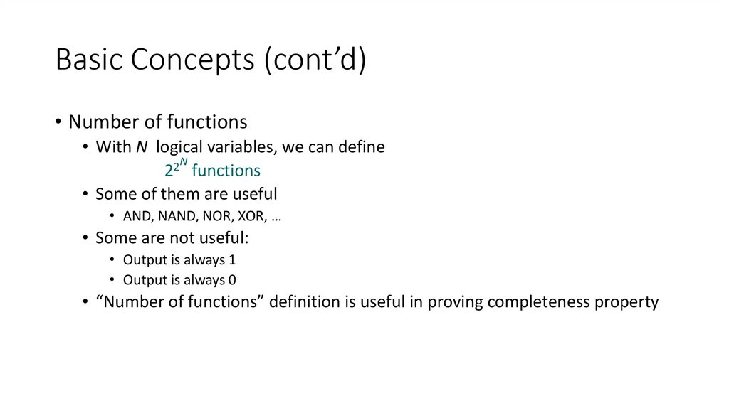
Basic Concepts (cont’d)• Number of functions
• With N logical variables, we can define
N
2
2 functions
• Some of them are useful
• AND, NAND, NOR, XOR, …
• Some are not useful:
• Output is always 1
• Output is always 0
• “Number of functions” definition is useful in proving completeness property
8.
Basic Concepts (cont’d)• Complete sets
• A set of gates is complete
• if we can implement any logical function using only the type of gates in the set
• You can uses as many gates as you want
• Some example complete sets
{AND, OR, NOT}
{AND, NOT}
{OR, NOT}
{NAND}
{NOR}
Not a minimal complete set
• Minimal complete set
• A complete set with no redundant elements.
9.
Basic Concepts (cont’d)• Proving NAND gate is universal
10.
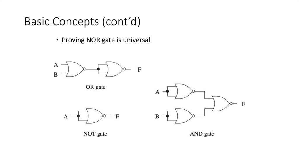
Basic Concepts (cont’d)• Proving NOR gate is universal
11.
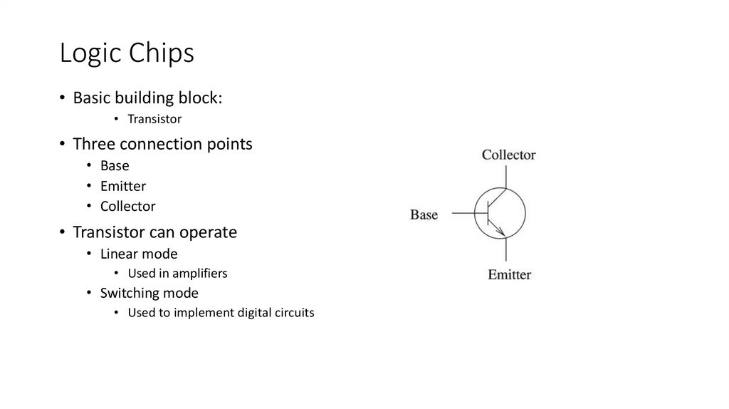
Logic Chips• Basic building block:
• Transistor
• Three connection points
• Base
• Emitter
• Collector
• Transistor can operate
• Linear mode
• Used in amplifiers
• Switching mode
• Used to implement digital circuits
12.
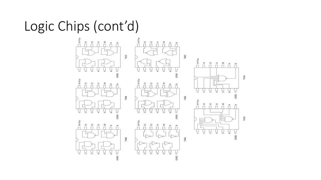
Logic Chips (cont’d)NOT
NAND
NOR
13.
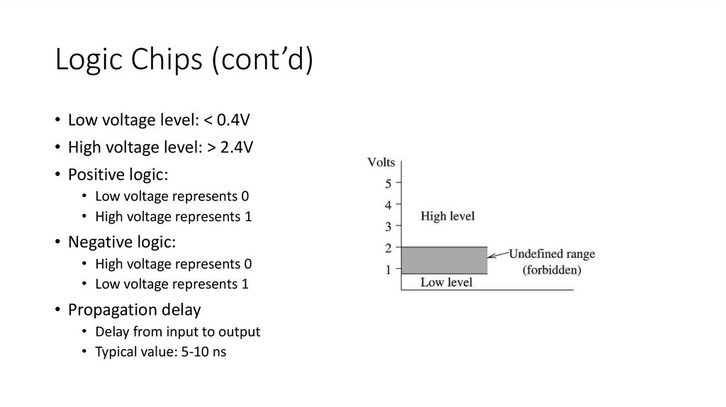
Logic Chips (cont’d)• Low voltage level: < 0.4V
• High voltage level: > 2.4V
• Positive logic:
• Low voltage represents 0
• High voltage represents 1
• Negative logic:
• High voltage represents 0
• Low voltage represents 1
• Propagation delay
• Delay from input to output
• Typical value: 5-10 ns
14.
Logic Chips (cont’d)15.
Logic Chips (cont’d)• Integration levels
• SSI (small scale integration)
• Introduced in late 1960s
• 1-10 gates (previous examples)
• MSI (medium scale integration)
• Introduced in late 1960s
• 10-100 gates
• LSI (large scale integration)
• Introduced in early 1970s
• 100-10,000 gates
• VLSI (very large scale integration)
• Introduced in late 1970s
• More than 10,000 gates
16.
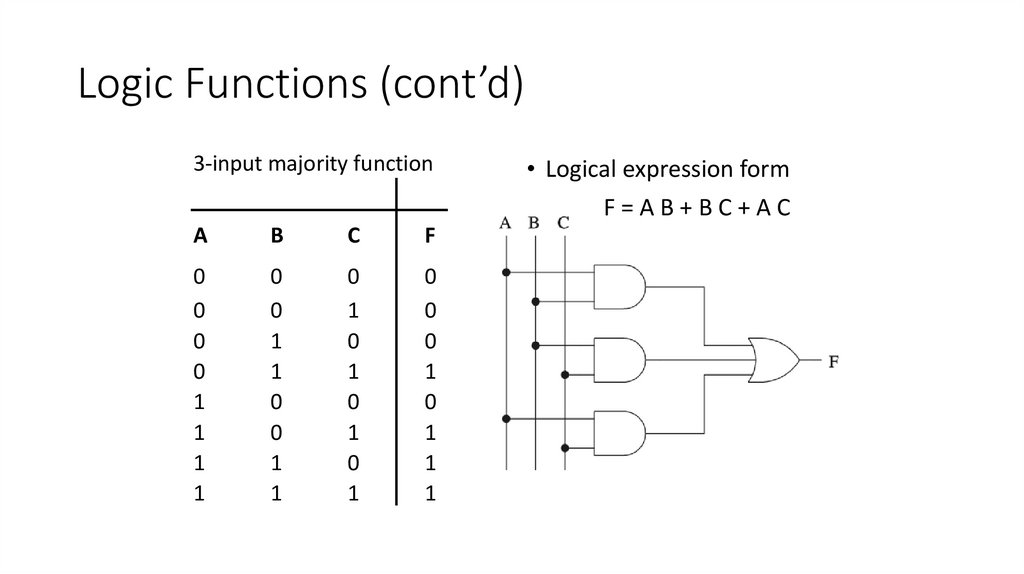
Logic Functions• Logical functions can be expressed in several ways:
• Truth table
• Logical expressions
• Graphical form
• Example:
• Majority function
• Output is one whenever majority of inputs is 1
• We use 3-input majority function
17.
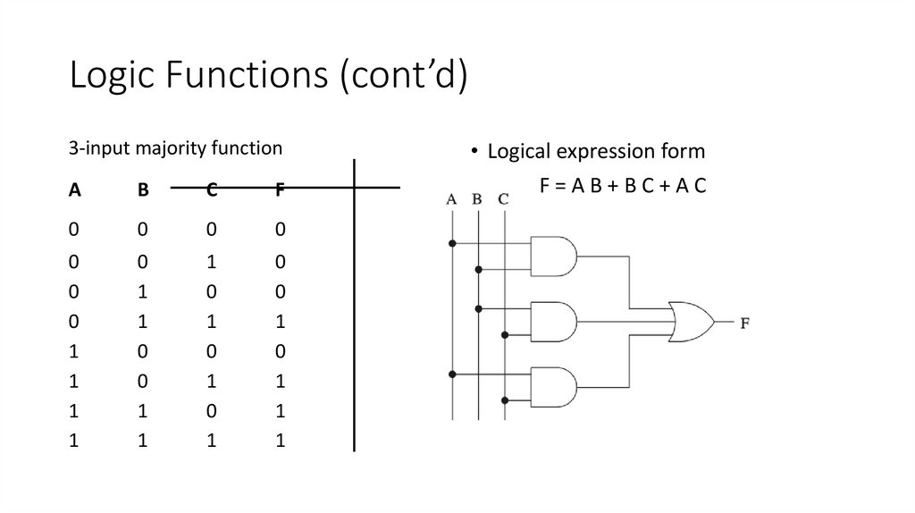
Logic Functions (cont’d)3-input majority function
A
B
C
F
0
0
0
0
0
0
0
1
1
1
1
0
1
1
0
0
1
1
1
0
1
0
1
0
1
0
0
1
0
1
1
1
• Logical expression form
F=AB+BC+AC
18.
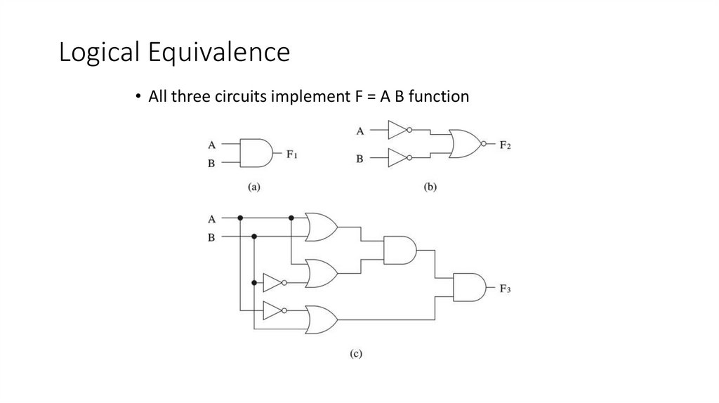
Logical Equivalence• All three circuits implement F = A B function
19.
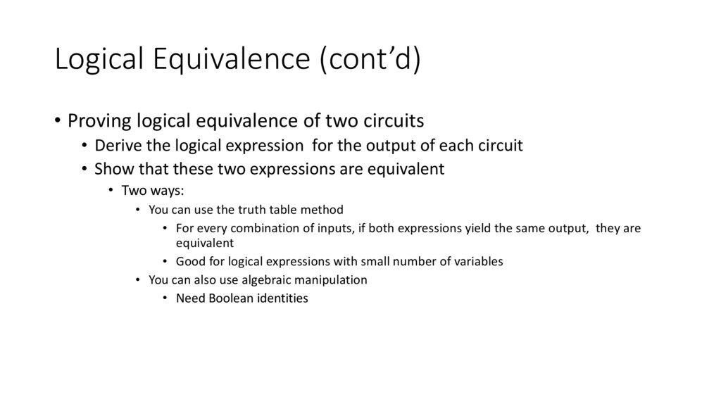
Logical Equivalence (cont’d)• Proving logical equivalence of two circuits
• Derive the logical expression for the output of each circuit
• Show that these two expressions are equivalent
• Two ways:
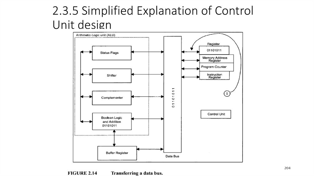
• You can use the truth table method
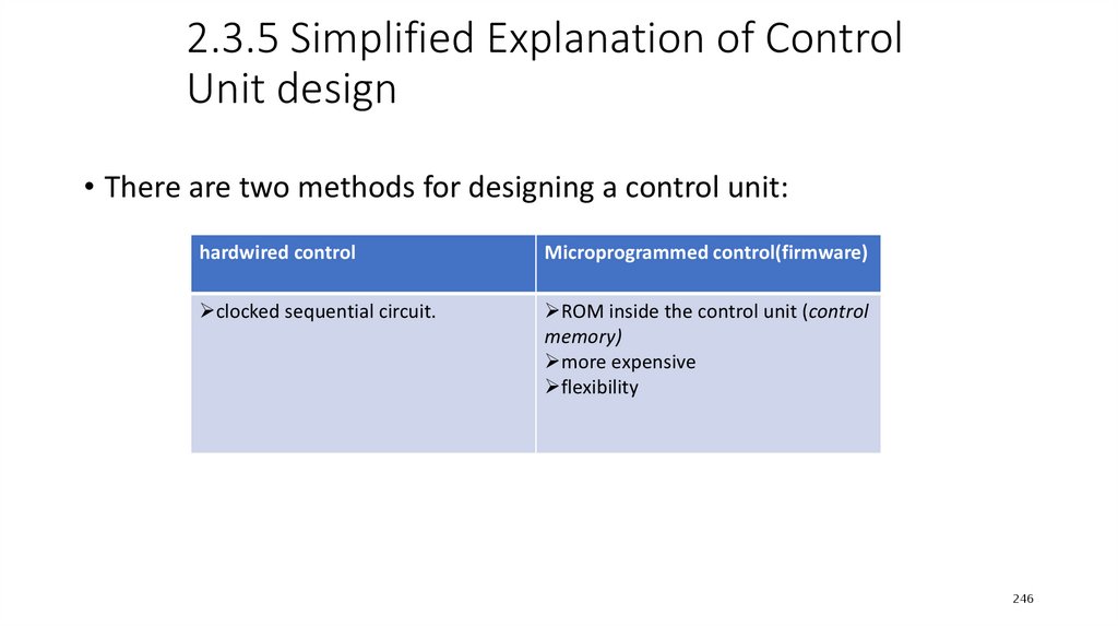
• For every combination of inputs, if both expressions yield the same output, they are
equivalent
• Good for logical expressions with small number of variables
• You can also use algebraic manipulation
• Need Boolean identities
20.
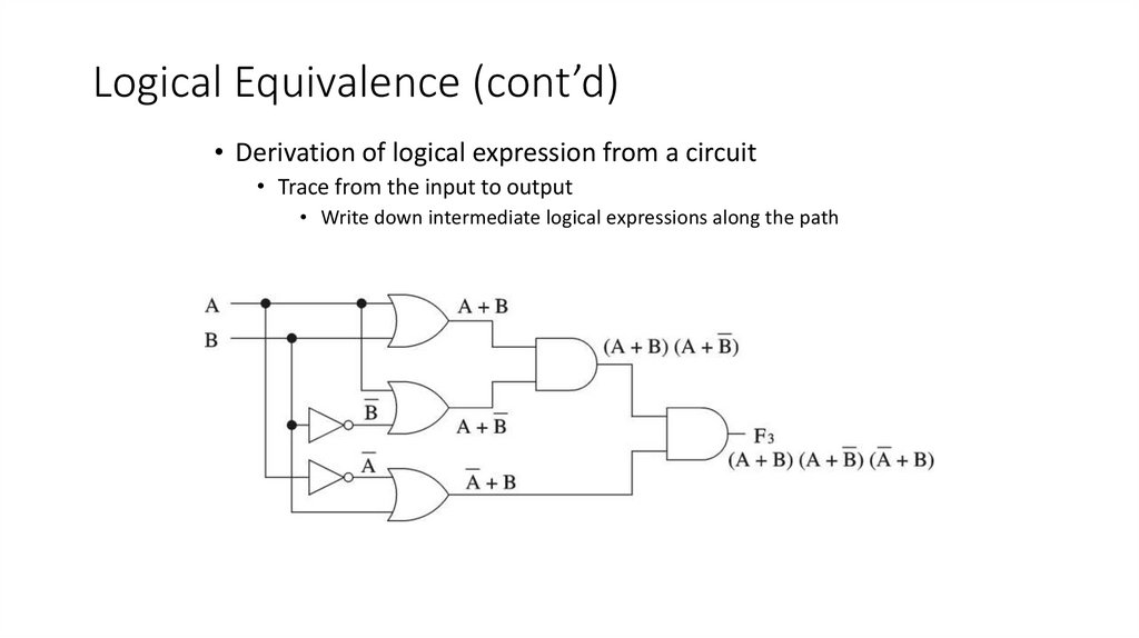
Logical Equivalence (cont’d)• Derivation of logical expression from a circuit
• Trace from the input to output
• Write down intermediate logical expressions along the path
21.
Logical Equivalence (cont’d)• Proving logical equivalence: Truth table method
A
0
0
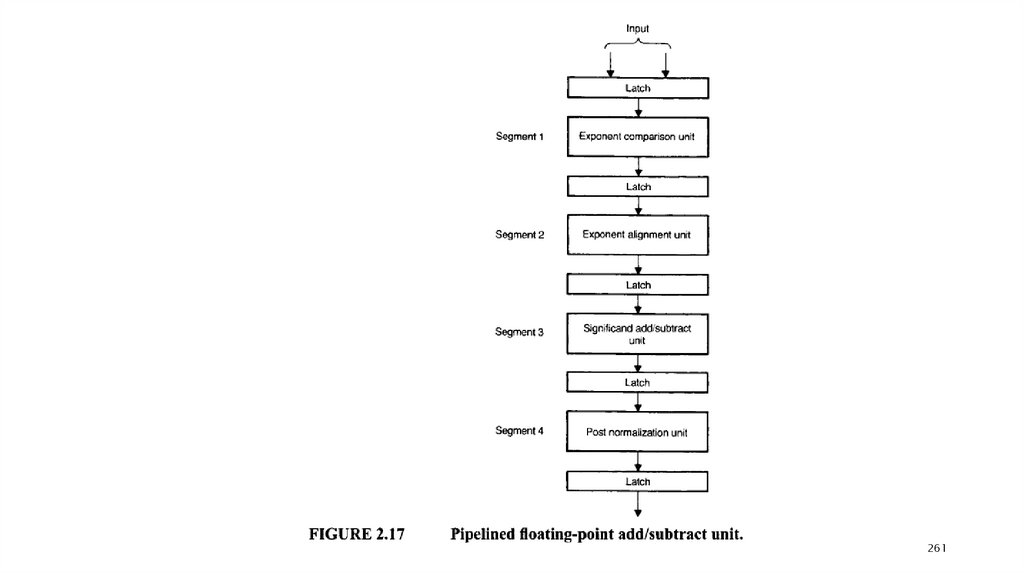
1
1
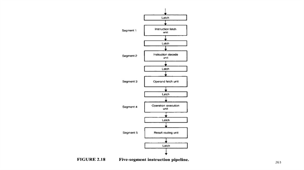
B
0
1
0
1
F1 = A B
0
0
0
1
F3 = (A + B) (A + B) (A + B)
0
0
0
1
22.
Thanks for yourattention
23.
LECTURE 224.
FUNDAMENTALSOF LOGICAL DESIGN
Dana Utebayeva
SIS 2
“Binary systems”
d.utebayeva@iitu.edu.kz
25.
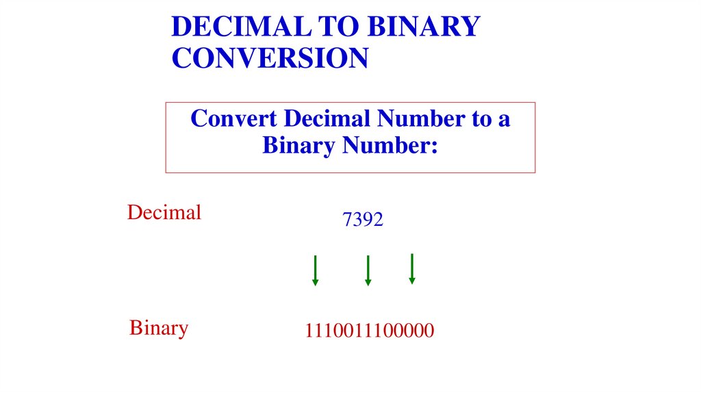
DECIMAL TO BINARYCONVERSION
Convert Decimal Number to a
Binary Number:
Decimal
Binary
7392
1110011100000
26.
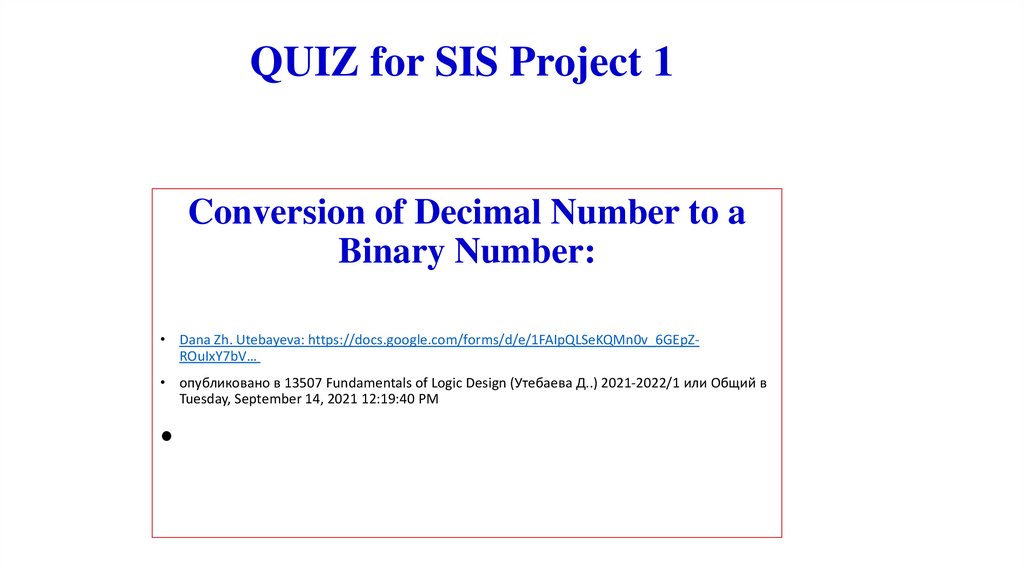
QUIZ for SIS Project 1Conversion of Decimal Number to a
Binary Number:
• Dana Zh. Utebayeva: https://docs.google.com/forms/d/e/1FAIpQLSeKQMn0v_6GEpZROuIxY7bV…
• опубликовано в 13507 Fundamentals of Logic Design (Утебаева Д..) 2021-2022/1 или Общий в
Tuesday, September 14, 2021 12:19:40 PM
27.
FUNDAMENTALSOF LOGICAL DESIGN
Dana Utebayeva
Lecture 2
“Number systems and Codes”
d.utebayeva@iitu.edu.kz
28.
• Goal of the lecture is to be familiar with numbersystems and code in digital electronics.
29.
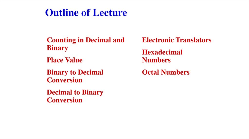
Outline of Lecture• Counting in Decimal and
Binary
• Place Value
• Binary to Decimal
Conversion
• Decimal to Binary
Conversion
• Electronic Translators
• Hexadecimal
Numbers
• Octal Numbers
30.
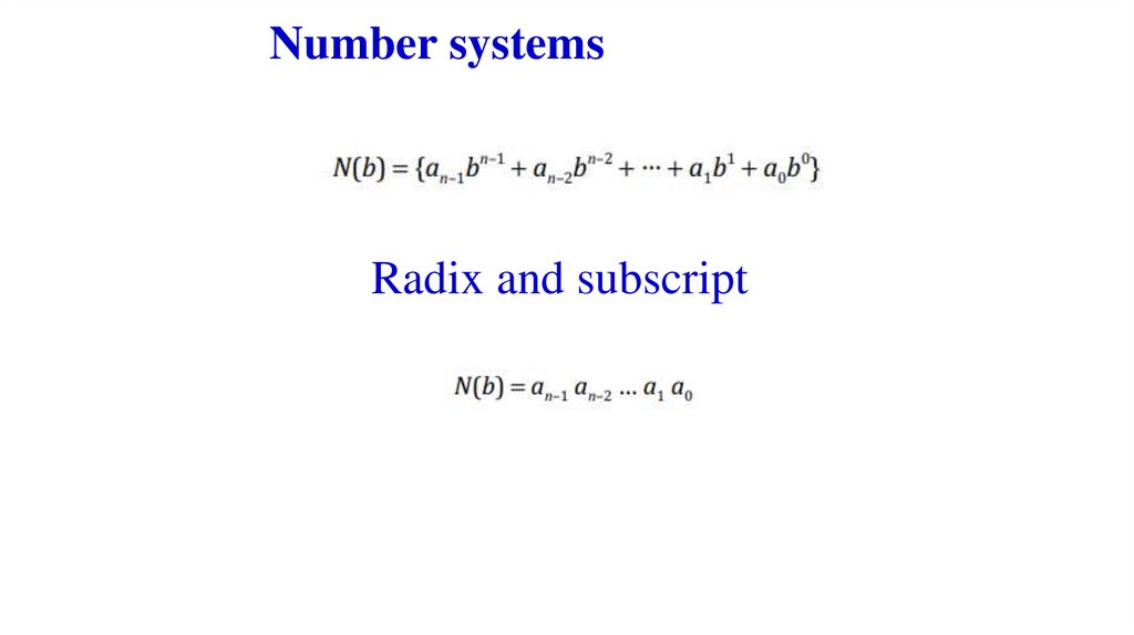
Number systemsRadix and subscript
31.
COUNTING INDECIMAL AND BINARY
• Number System Code using symbols that refer to
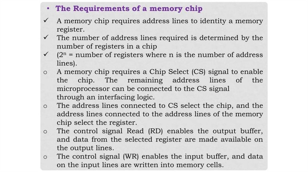
a number of items.
• Decimal Number System Uses ten symbols (base 10 system)
• Binary System Uses two symbols (base 2 system)
32.
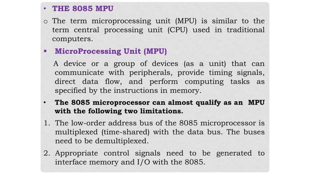
Generalized approach ofNumber systems
A number with a decimal point is
represented by series of
coefficients
33.
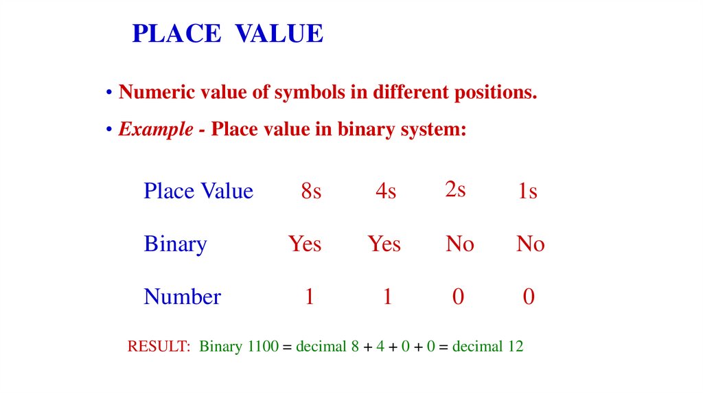
PLACE VALUE• Numeric value of symbols in different positions.
• Example - Place value in binary system:
8s
4s
2s
1s
Binary
Yes
Yes
No
No
Number
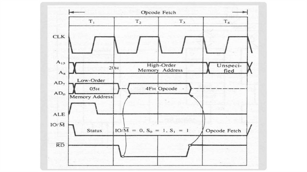
1
1
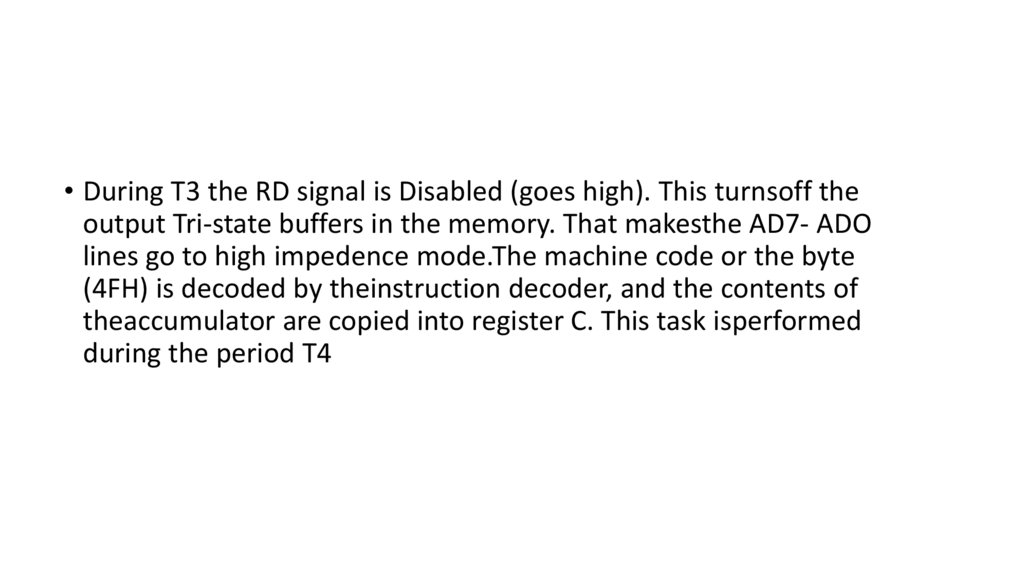
0
0
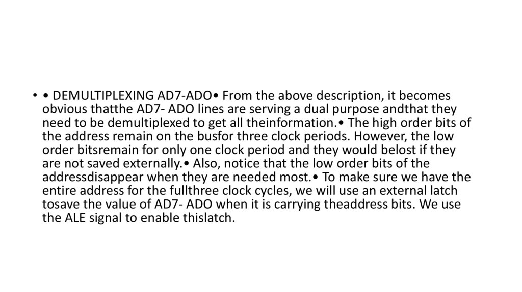
Place Value
RESULT: Binary 1100 = decimal 8 + 4 + 0 + 0 = decimal 12
34.
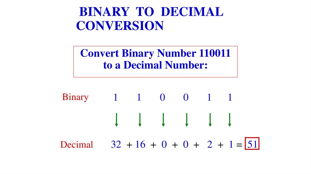
BINARY TO DECIMALCONVERSION
Convert Binary Number 110011
to a Decimal Number:
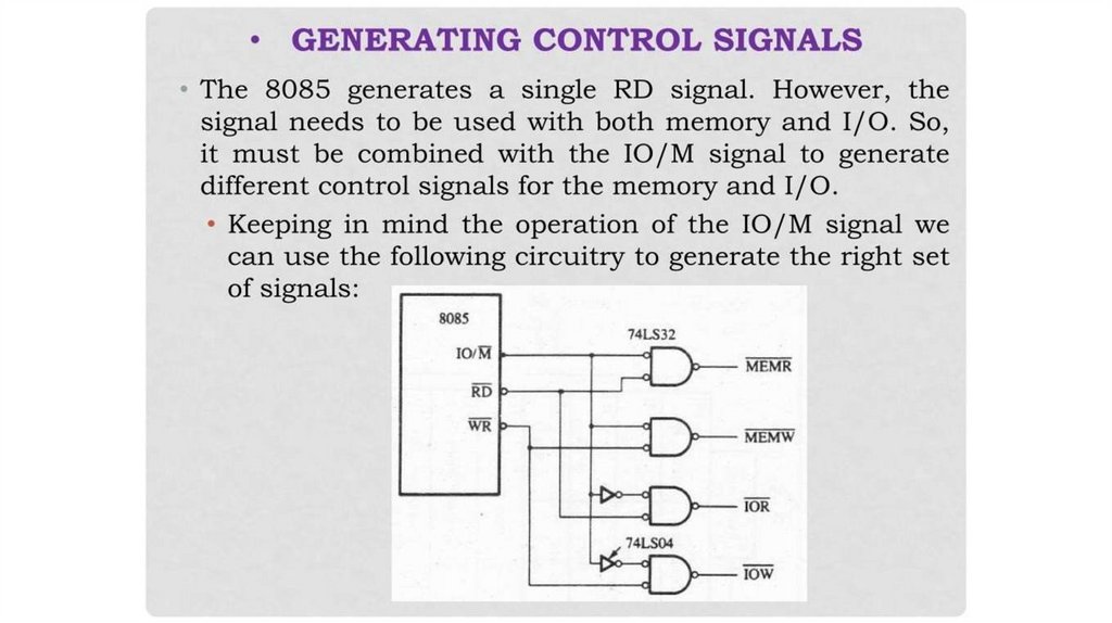
Binary
1
Decimal
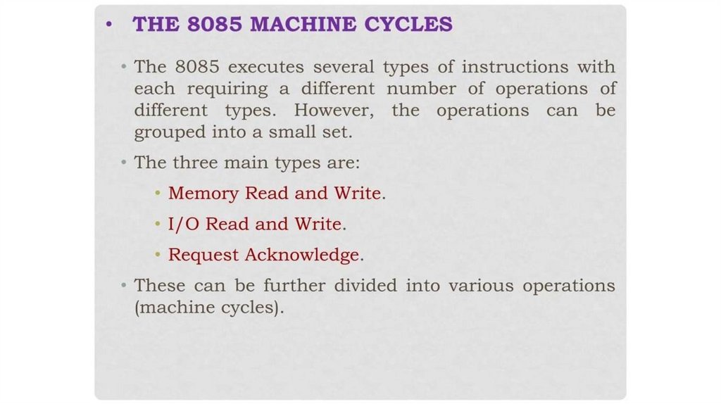
32 + 16 + 0 + 0 + 2 + 1 = 51
1
0
0
1
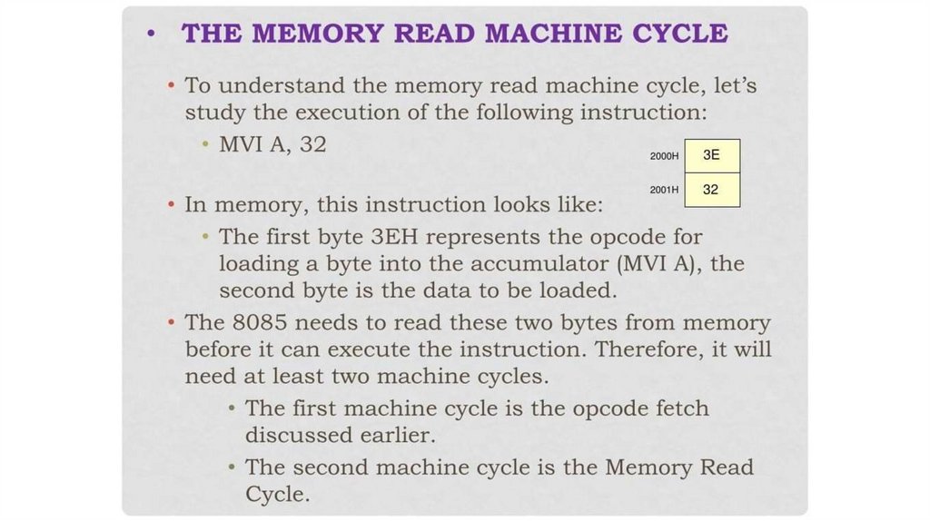
1
35.
TESTConvert the following binary
numbers into decimal numbers:
Binary 1001 =
9
Binary 1111 =
15
Binary 0010 =
2
36.
DECIMAL TO BINARYCONVERSION
Divide by 2 Process
Decimal # 13 ÷ 2 = 6 remainder 1
6 ÷ 2 = 3 remainder 0
3 ÷ 2 = 1 remainder 1
1 ÷ 2 = 0 remainder 1
1
1 0 1
37.
TESTConvert the following decimal
numbers into binary:
Decimal 11 =
1011
Decimal 4
0100
=
Decimal 17 = 10001
38.
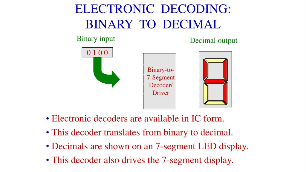
ELECTRONIC TRANSLATORSDevices that convert from decimal to
binary numbers and from binary to
decimal numbers.
Encoders translates from decimal to binary
Decoders translates from binary to decimal
39.
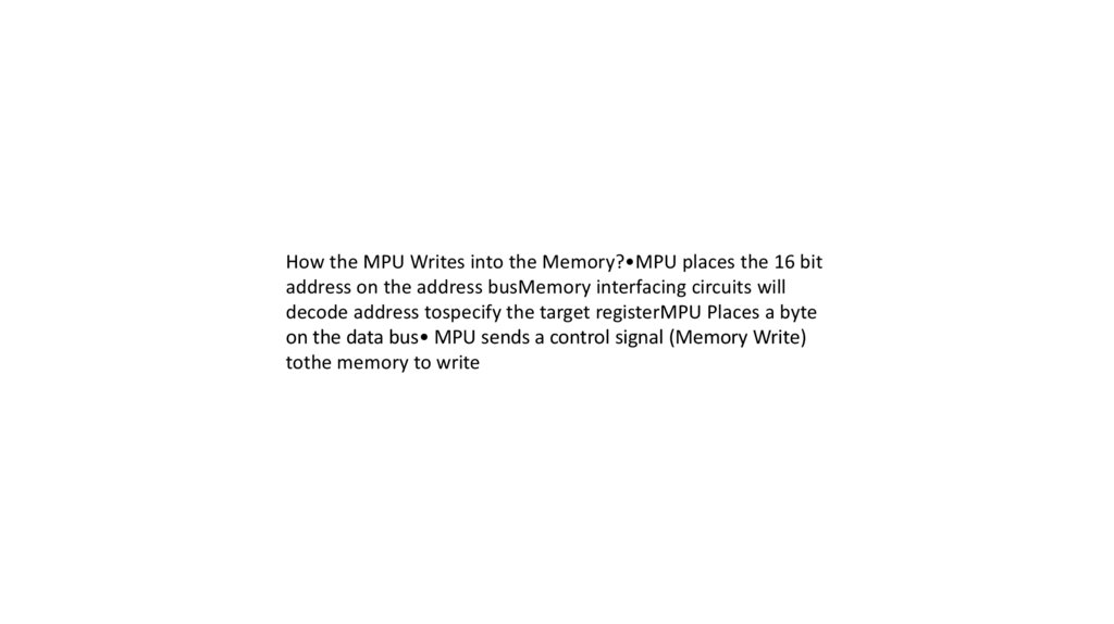
ELECTRONIC ENCODER DECIMAL TO BINARYBinary output
Decimal input
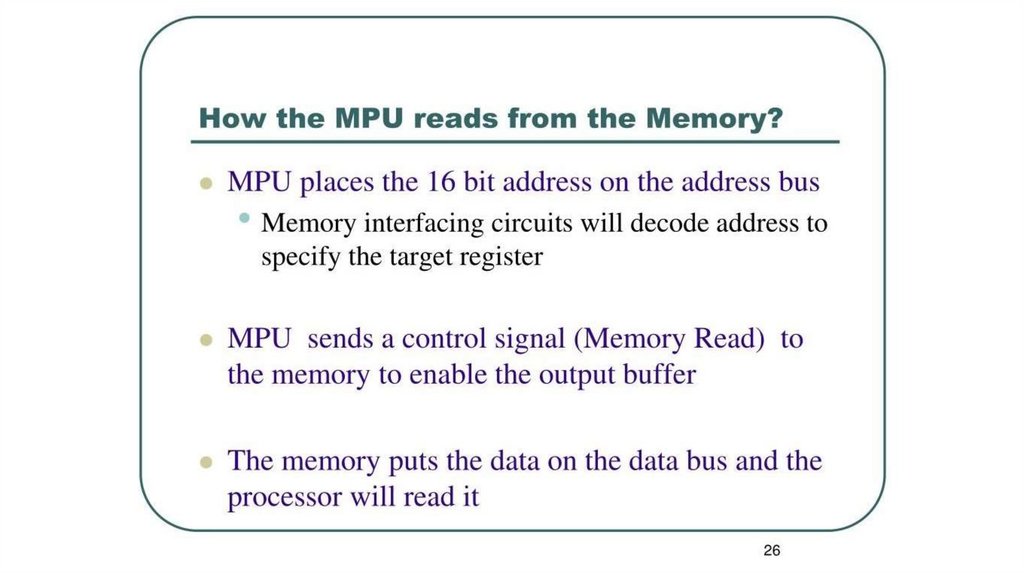
7
5
3
0
01
0
00
11
Decimal
to
Binary
Encoder
• Encoders are available in IC form.
• This encoder translates from decimal input
to binary (BCD) output.
40.
ELECTRONIC DECODING:BINARY TO DECIMAL
Binary input
Decimal output
0 10 01 01
Binary-to7-Segment
Decoder/
Driver
• Electronic decoders are available in IC form.
• This decoder translates from binary to decimal.
• Decimals are shown on an 7-segment LED display.
• This decoder also drives the 7-segment display.
41.
HEXADECIMAL NUMBER SYSTEMUses 16 symbols -Base 16 System
0-9, A, B, C, D, E, F
Decimal
1
9
10
15
16
Binary
0001
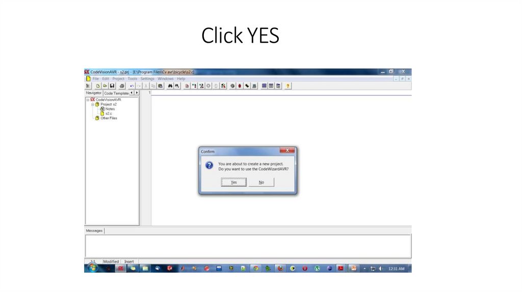
1001
1010
1111
10000
Hexadecimal
1
9
A
F
10
42.
HEXADECIMAL ANDBINARY CONVERSIONS
•Hexadecimal to Binary Conversion
Hexadecimal
C
3
Binary
1100
0011
•Binary to Hexadecimal Conversion
Binary
1110
Hexadecimal
1010
E
A
43.
DECIMAL TO HEXADECIMALCONVERSION
Divide by 16 Process
Decimal #
47 ÷ 16 = 2 remainder 15
2 ÷ 16 = 0 remainder 2
2
F
44.
HEXADECIMAL TO DECIMALCONVERSION
Convert hexadecimal number 2DB
to a decimal number
Place Value
256s
Hexadecimal
Decimal
16s
1s
2
D
B
(256 x 2)
(16 x 13)
(1 x 11)
512
+
208
+
11
= 731
45.
TESTConvert Hexadecimal number A6 to Binary
A6 =
1010 0110 (Binary)
Convert Hexadecimal number 16 to Decimal
16 =
22 (Decimal)
Convert Decimal 63 to Hexadecimal
63 = 3F (Hexadecimal)
46.
OCTAL NUMBERSUses 8 symbols -Base 8 System
0, 1, 2, 3, 4, 5, 6, 7
Decimal
1
6
7
8
9
Binary
001
110
111
001 000
001 001
Octal
1
6
7
10
11
47.
PRACTICAL SUGGESTION ONNUMBER SYSTEM CONVERSIONS
• Use a scientific calculator
• Most scientific calculators have DEC, BIN,
OCT, and HEX modes and can either
convert between codes or perform
arithmetic in different number systems.
• Most scientific calculators also have other
functions that are valuable in digital
electronics such as AND, OR, NOT,
XOR, and XNOR logic functions.
48.
SIS project 1• 1) first page (Names, Title: “Binary systems”)
• 2) Outline (План)
• 3) Part I: (images from your “конспект”)
• 4) Part II: Upload/insert your screens from your
Quiz
• 5) Part: Assignments: screens from your copybook
• 6) About calculators
Deadline: Monday till 18.oo (20.09.2021)
49.
Attendance for Lecture 2• Dana Zh. Utebayeva:
https://docs.google.com/forms/d/e/1FAIpQLSfotGeOUvqjykd78SYCT_
WEU…
• опубликовано в 13507 Fundamentals of Logic Design (Утебаева Д..)
2021-2022/1 или Общий в Tuesday, September 14, 2021 1:46:25 PM
50.
LECTURE 3-451.
Outline• Binary numbers
• Logic States
• Implementation
• The Buffer Logic Gate using n-pn transistors
• Logic Gates using transistors
• Logic functions
• Expressing logic functions
• Building block diagrams
• Boolean algebra
• Boolean algebra laws
• Logic Circuit Design Process
• Deriving logical expressions
• Sum-of-products form
• Product-of-sums form
• Generalized gates
• Multiple outputs
• Implementation using other
gates (NAND and XOR)
52.
POS – product of sums53.
Logic Gates• Simple gates
• AND
• OR
• NOT
• Functionality can be expressed by a
truth table
• A truth table lists output for each
possible input combination
• Other methods
• Logic expressions
• Logic diagrams
54.
Basic Concepts (cont’d)• Additional useful gates
• NAND
• NOR
• XOR
• NAND = AND + NOT
• NOR = OR + NOT
• XOR implements exclusive-OR
function
• NAND and NOR gates require only 2
transistors
• AND and OR need 3 transistors!
55.
Basic Concepts (cont’d)• Number of functions
• With N logical variables, we can define
N
2
2 functions
• Some of them are useful
• AND, NAND, NOR, XOR, …
• Some are not useful:
• Output is always 1
• Output is always 0
• “Number of functions” definition is useful in proving completeness property
56.
Basic Concepts (cont’d)• Complete sets
• A set of gates is complete
• if we can implement any logical function using only the type of gates in the set
• You can uses as many gates as you want
• Some example complete sets
{AND, OR, NOT}
{AND, NOT}
{OR, NOT}
{NAND}
{NOR}
Not a minimal complete set
• Minimal complete set
• A complete set with no redundant elements.
57.
Basic Concepts (cont’d)• Proving NAND gate is universal
58.
Basic Concepts (cont’d)• Proving NOR gate is universal
59.
Logic Chips• Basic building block:
• Transistor
• Three connection points
• Base
• Emitter
• Collector
• Transistor can operate
• Linear mode
• Used in amplifiers
• Switching mode
• Used to implement digital circuits
60.
Logic Chips (cont’d)NOT
NAND
NOR
61.
Logic Chips (cont’d)• Low voltage level: < 0.4V
• High voltage level: > 2.4V
• Positive logic:
• Low voltage represents 0
• High voltage represents 1
• Negative logic:
• High voltage represents 0
• Low voltage represents 1
• Propagation delay
• Delay from input to output
• Typical value: 5-10 ns
62.
Logic Chips (cont’d)63.
Logic Chips (cont’d)• Integration levels
• SSI (small scale integration)
• Introduced in late 1960s
• 1-10 gates (previous examples)
• MSI (medium scale integration)
• Introduced in late 1960s
• 10-100 gates
• LSI (large scale integration)
• Introduced in early 1970s
• 100-10,000 gates
• VLSI (very large scale integration)
• Introduced in late 1970s
• More than 10,000 gates
64.
Logic Functions• Logical functions can be expressed in several ways:
• Truth table
• Logical expressions
• Graphical form
• Example:
• Majority function
• Output is one whenever majority of inputs is 1
• We use 3-input majority function
65.
Logic Functions (cont’d)3-input majority function
• Logical expression form
F=AB+BC+AC
A
B
C
F
0
0
0
0
1
1
1
1
0
0
1
1
0
0
1
1
0
1
0
1
0
1
0
1
0
0
0
1
0
1
1
1
66.
Logical Equivalence• All three circuits implement F = A B function
67.
Logical Equivalence (cont’d)• Proving logical equivalence of two circuits
• Derive the logical expression for the output of each circuit
• Show that these two expressions are equivalent
• Two ways:
• You can use the truth table method
• For every combination of inputs, if both expressions yield the same output, they are
equivalent
• Good for logical expressions with small number of variables
• You can also use algebraic manipulation
• Need Boolean identities
68.
Logical Equivalence (cont’d)• Derivation of logical expression from a circuit
• Trace from the input to output
• Write down intermediate logical expressions along the path
69.
Logical Equivalence (cont’d)• Proving logical equivalence: Truth table method
A
0
0
1
1
B
0
1
0
1
F1 = A B
0
0
0
1
F3 = (A + B) (A + B) (A + B)
0
0
0
1
70.
Thanks for yourattention
71.
LECTURE 472.
#3 Boolean Algebra and Digital Logic Gates.#4 Combinational logic design. Completely and Incompletely
Specified Logic Functions. Design of a combinational Circuits.
Lecture 3 - 4
Dana Utebayeva
73.
Outline• Binary numbers
• Logic States
• Implementation
• The Buffer Logic Gate using n-pn transistors
• Logic Gates using transistors
• Logic functions
• Expressing logic functions
• Building block diagrams
• Boolean algebra
• Boolean algebra laws
• Logic Circuit Design Process
• Deriving logical expressions
• Sum-of-products form
• Product-of-sums form
• Generalized gates
• Multiple outputs
• Implementation using other
gates (NAND and XOR)
74.
Basic Concepts (cont’d)• Number of functions
• With N logical variables, we can define
N
2
2 functions
• Some of them are useful
• AND, NAND, NOR, XOR, …
• Some are not useful:
• Output is always 1
• Output is always 0
• “Number of functions” definition is useful in proving completeness property
75.
Basic Concepts (cont’d)• Complete sets
• A set of gates is complete
• if we can implement any logical function using only the type of gates in the set
• You can uses as many gates as you want
• Some example complete sets
{AND, OR, NOT}
{AND, NOT}
{OR, NOT}
{NAND}
{NOR}
Not a minimal complete set
• Minimal complete set
• A complete set with no redundant elements.
76.
Basic Concepts (cont’d)• Proving NAND gate is universal
77.
Basic Concepts (cont’d)• Proving NOR gate is universal
78.
Logic Chips• Basic building block:
• Transistor
• Three connection points
• Base
• Emitter
• Collector
• Transistor can operate
• Linear mode
• Used in amplifiers
• Switching mode
• Used to implement digital circuits
79.
Logic Chips (cont’d)NOT
NAND
NOR
80.
Logic Chips (cont’d)• Low voltage level: < 0.4V
• High voltage level: > 2.4V
• Positive logic:
• Low voltage represents 0
• High voltage represents 1
• Negative logic:
• High voltage represents 0
• Low voltage represents 1
• Propagation delay
• Delay from input to output
• Typical value: 5-10 ns
81.
Logic Chips (cont’d)82.
Logic Chips (cont’d)• Integration levels
• SSI (small scale integration)
• Introduced in late 1960s
• 1-10 gates (previous examples)
• MSI (medium scale integration)
• Introduced in late 1960s
• 10-100 gates
• LSI (large scale integration)
• Introduced in early 1970s
• 100-10,000 gates
• VLSI (very large scale integration)
• Introduced in late 1970s
• More than 10,000 gates
83.
Logic Functions• Logical functions can be expressed in several ways:
• Truth table
• Logical expressions
• Graphical form
• Example:
• Majority function
• Output is one whenever majority of inputs is 1
• We use 3-input majority function
84.
Logic Functions (cont’d)3-input majority function
A
B
C
F
0
0
0
0
0
0
0
1
1
1
1
0
1
1
0
0
1
1
1
0
1
0
1
0
1
0
0
1
0
1
1
1
• Logical expression form
F=AB+BC+AC
85.
Logical Equivalence• All three circuits implement F = A B function
86.
Logical Equivalence (cont’d)• Proving logical equivalence of two circuits
• Derive the logical expression for the output of each circuit
• Show that these two expressions are equivalent
• Two ways:
• You can use the truth table method
• For every combination of inputs, if both expressions yield the same output, they are
equivalent
• Good for logical expressions with small number of variables
• You can also use algebraic manipulation
• Need Boolean identities
87.
Logical Equivalence (cont’d)• Derivation of logical expression from a circuit
• Trace from the input to output
• Write down intermediate logical expressions along the path
88.
Logical Equivalence (cont’d)• Proving logical equivalence: Truth table method
A
0
0
1
1
B
0
1
0
1
F1 = A B
0
0
0
1
F3 = (A + B) (A + B) (A + B)
0
0
0
1
89.
Thanks for yourattention
90.
LECTURE 591.
«СРС»: SIS, Practice class and Lab class assignmentsexplanation
#5 Combinational and Sequential Circuit.
Adders. Subtractors. Comparators.
Lecture 5
Dana Utebayeva
92.
Outline• «СРС» SIS assignments
explanation
• Practice class
• Lab class
• SIS assignments explanation
• Standard Representations
Minterm
Maxterm
• Combinational and
Sequential circuits
• Boolean
Identities/Postulates/laws • Adders
• Expressing logic functions
• Building block diagrams
• Simplification Using
Boolean Identities
• Comparators
• Full Subtractor
93.
Boolean Identities / Postulates / lawsBoolean Laws
94.
Problem 2(a) Implementation of f= ABCD +
ABCD + BC(b) implementation
of the simplified function f= BC
+ DImplementation of Boolean
function using logic gates
95.
96.
Simplification Using Boolean Identitiesf= ABCD + ABCD + BC
97.
98.
Complement of a Boolean Function(А + В + С)
99.
Complement of a Boolean Functionf= C'(AB + A'B'D + A'BD')
f= C(AB + ABD + ABD)
100.
Combinational and Sequentialcircuits
101.
102.
103.
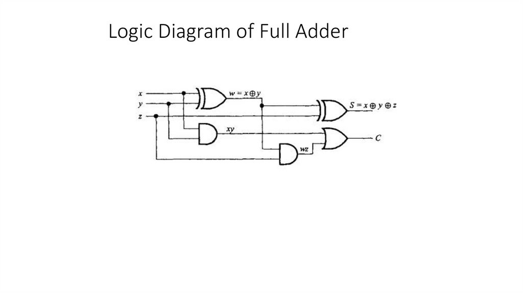
Full Adder104.
Logic Diagram of Full Adder105.
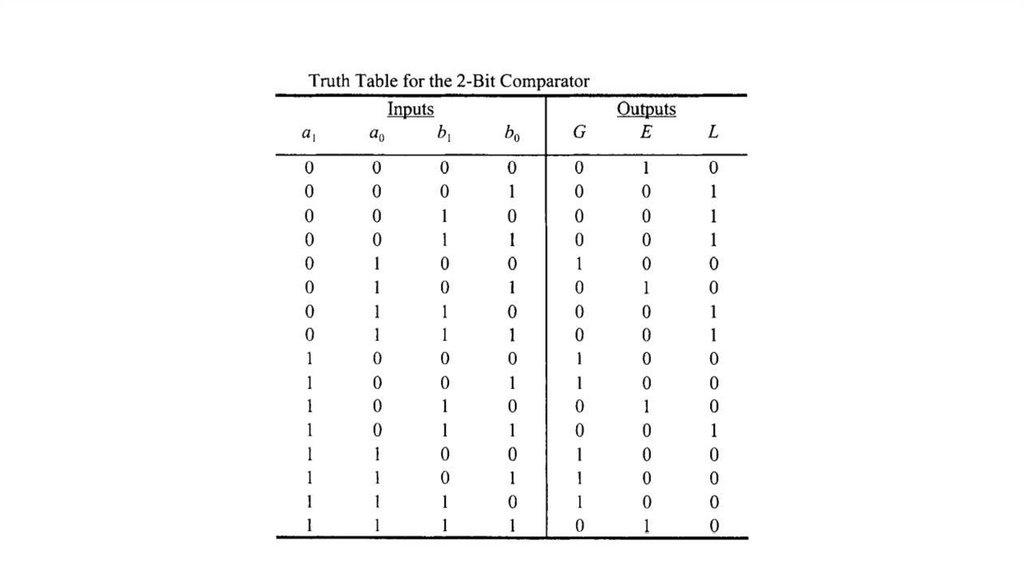
Two-bit Comparator106.
107.
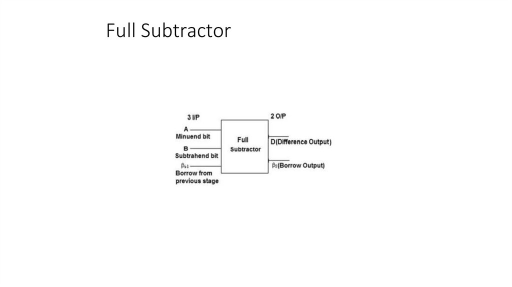
Full Subtractor108.
Logic Chips (cont’d)• Integration levels
• SSI (small scale integration)
• Introduced in late 1960s
• 1-10 gates (previous examples)
• MSI (medium scale integration)
• Introduced in late 1960s
• 10-100 gates
• LSI (large scale integration)
• Introduced in early 1970s
• 100-10,000 gates
• VLSI (very large scale integration)
• Introduced in late 1970s
• More than 10,000 gates
109.
LECTURE 6110.
Multiplexer designProcedure and applications
Lecture 6
Utebayeva dana
111.
112.
113.
114.
115.
116.
117.
118.
Truth table for MUXTruth table for 4-to-1 MUX
119.
LECTURE 7120.
Demultiplexers and theirApplications
Lecture 7, By dana Utebayeva
121.
DEMUX DEMULTIPLEXER122.
123.
124.
125.
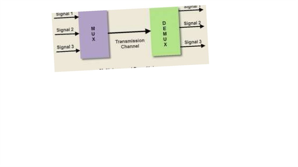
MUX and DEMUXapplications
126.
MUX and DEMUX applications127.
128.
LECTURE 8 K-MAP K MAPKMAP
129.
Introduction to Karnaughmap (k-map)
СРС (SIS) by Dana Utebayeva
130.
131.
132.
133.
134.
135.
136.
137.
LECTURE 9138.
Sequential Circuit.Sequential logic
design. Flip-Flop.
Counters
Lecture 9
By Dana Utebayeva
139.
Sequential Circuit. Sequential logic design. Flip-Flop. CountersLATCHES
FLIP-FLOPS
WHAT IS THE CLOCK?
140.
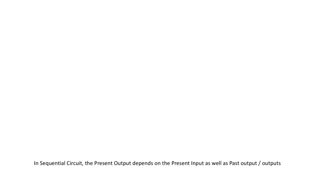
In Sequential Circuit, the Present Output depends on the Present Input as well as Past output / outputs141.
142.
Cascaded NOT logic gate143.
The basic storage element is called latch144.
145.
146.
147.
148.
149.
150.
151.
LECTURE 11-12152.
Lecture 10-11MICROCOMPUTER ARCHITECTURE
Memory
ADC and DAC
152
153.
Outline• ADC and DAC
• 1.1 Basic Blocks of a Microcomputer
• 1.2 Typical Microcomputer Architecture
• 1.3 Single-Chip Microprocessor
• 1.4 Program Execution by Conventional Microprocessors
• 1.5 Program Execution by typical 32-bit Microprocessors
• 1.6 Scalar and Superscalar Microprocessors
• 1.7 RISC vs. CISC
153
154.
ADC154
155.
ADC and DACWork use of ADC and DAC
Sound Waves Electrical Voltage Binary Data Electrical Voltage Sound Waves
155
156.
Need Conversation156
157.
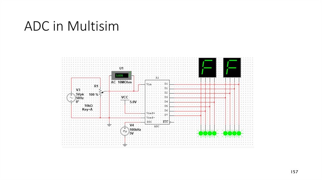
ADC in Multisim157
158.
DACDAC scheme DAC circuit
158
159.
2.1 Basic Blocks of a MicrocomputerA microcomputer has three basic blocks: a central processing unit
(CPU), a memory unit,
and an input/output (I/O) unit.
The CPU(microprocessor) executes all the instructions and performs
arithmetic and logic operations on data.
A memory unit stores both data and instructions. The memory
section typically
contains ROM and RAM chips.
A system bus (comprised of several wires) connects these blocks.
159
160.
2.1 Basic Blocks of a MicrocomputerSystem bus
160
161.
2.1 Basic Blocks of a Microcomputer• In a single-chip microcomputer, these three elements are on one chip,
whereas
• in a single-chip microprocessor, separate chips are required for
memory and I/O.
161
162.
2.2 Typical Microcomputer ArchitectureSimplified version of typical microprocessor
162
163.
2.2.1 System BusThe microcomputer’s system bus contains three buses, address,
data, and control bus
When a memory or an I/O chip receives data from the
microprocessor, it is called a WRITE operation, and data is written
into a selected memory location or an I/O port (register).
When a memory or an I/O chip sends data to the microprocessor, it
is called a READ operation, and data is read from a selected memory
location or an I/O port.
163
164.
2.2.1 System BusThe Address Bus
1. Unidirectional bus: Information transfer takes place in only one
direction, from the microprocessor to the memory or I/O elements.
2. Typically 20 to 32 bits long.
3. The size of the address bus determines the
total number of memory addresses available
For example : microprocessor with 32 address pins can
generate 232 = 4,294,964,296 bytes
164
165.
2.2.1 System BusThe data bus,
1. bidirectional bus: data can flow in both directions, that is, to or
from the microprocessor.
2. The size of the data bus varies from one microprocessor to
another.
165
166.
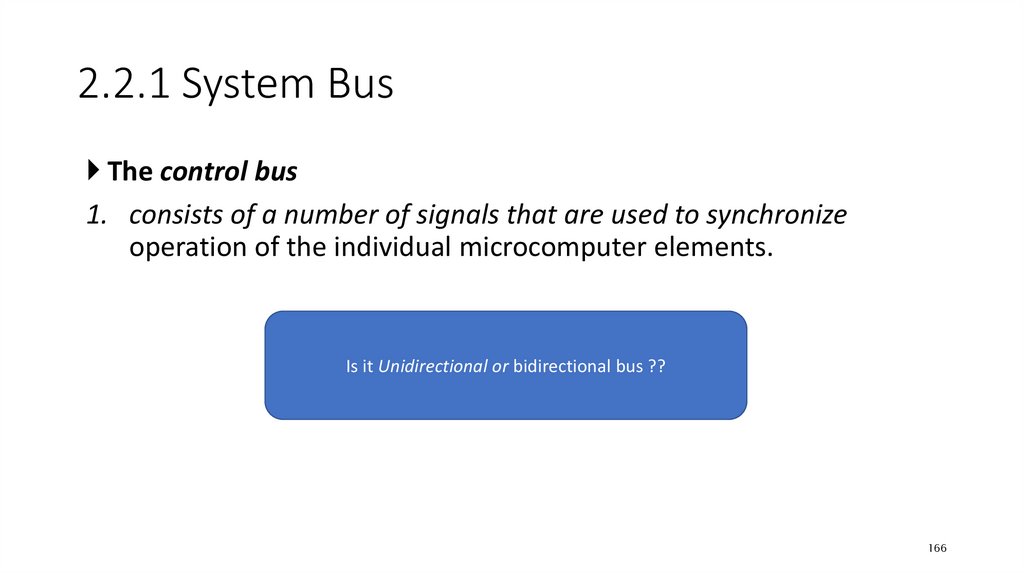
2.2.1 System BusThe control bus
1. consists of a number of signals that are used to synchronize
operation of the individual microcomputer elements.
Is it Unidirectional or bidirectional bus ??
166
167.
2.2.2 Clock SignalsThe system clock signals are contained in the control bus.
The number of cycles per second (hertz, abbreviated Hz) is referred to as the clock frequency.
• clock cycle = 1/f where f is the clock frequency.
• clock frequency determines the speed of the microcomputer.
167
168.
2.3 Single-Chip Microprocessor• The microprocessor is the CPU of the microcomputer
• The logic inside the microprocessor chip can be divided into three
main areas: the
register section, the control unit, and the arithmetic-logic unit (ALU).
168
169.
2.3.1 Register Section• The number, size, and types of registers vary from one
microprocessor to another.
• Basic Microprocessor Registers There are four basic microprocessor
registers: instruction register, program counter, memory address
register, and accumulator.
169
170.
2.3.1 Register Section• Instruction register (IR) :
The instruction register stores instructions.
The word size of the microprocessor determines the size of the
instruction register. For example, a 32-bit microprocessor has a 32-bit
instruction register.
170
171.
2.3.1 Register Section• Program Counter (PC):
The program counter contains the address of the instruction or
operation code (op-code).
The program counter normally contains the address of the next
instruction to be executed.
The size of the program counter is determined by the size of the
address bus.
171
172.
2.3.1 Register SectionHow Program Counter is Work ?
1.
Upon activating the microprocessor’s RESET input, the address of the first instruction to be
executed is loaded into the program counter.
2.
To execute an instruction, the microprocessor typically places the contents of the program
counter on the address bus and reads (“fetches”) the contents of this address(i.e., instruction)
from memory
3.
The program counter contents are incremented automatically by the microprocessor’s internal
logic. Microprocessor executes a program sequentially, unless the program contains an
instruction such as a JUMP instruction, which changes the sequence.
172
173.
2.3.1 Register Section• Memory Address Register (MAR).
The memory address register contains the address of data. The
microprocessor uses the address, which is stored in the memory
address register, as a direct pointer to memory. The contents of the
address is the actual data that is being transferred.
173
174.
2.3.1 Register Section• General Purpose Register (GPR). For an 8-bit microprocessor, the
general-purpose register is called the accumulator.
• It stores the result after most ALU operations.
• These 8-bit microprocessors have instructions to shift or rotate the
accumulator one bit to the right or left through the carry flag.
• In16- and 32-bit microprocessors the accumulator is replaced by a
GPR.
• any GPR can be used as an accumulator.
174
175.
2.3.1 Register Section• General Purpose Register (GPR).
The term general-purpose comes from the fact that these registers
can hold data, memory
addresses, or the results of arithmetic or logic operations.
• Most registers are general-purpose, but some, such as the program
counter (PC),are provided for dedicated functions.
175
176.
2.3.1 Register Section• Other Microprocessor Registers such as general-purpose registers,
index register, status register and stack pointer register.
• general-purpose registers speeds up the execution of a program because the microprocessor does not have
to read data from external memory via the data bus if data is stored in one of its general-purpose registers.
Index Register is typically used as a counter in address modification for an instruction or for general
storage functions. Used to access tables or arrays of data.
Status Register( a processor status word register or condition code register, contains individual bits, with
each bit having special significance. The bits in the status register are called flags.
176
177.
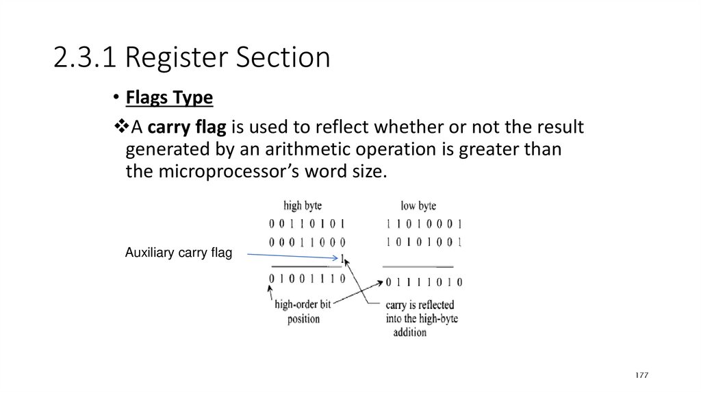
2.3.1 Register Section• Flags Type
A carry flag is used to reflect whether or not the result
generated by an arithmetic operation is greater than
the microprocessor’s word size.
Auxiliary carry flag
177
178.
2.3.1 Register Section• Flags Type
A zero flag is used to show whether the result of an operation is
zero. It is set to1 if the result is zero, and it is reset to 0 if the result is
nonzero.
A parity flag is set to 1 to indicate whether the result of the last
operation contains either an even number of 1’s (even parity) or an
odd number of 1’s (odd parity), depending on the microprocessor.
178
179.
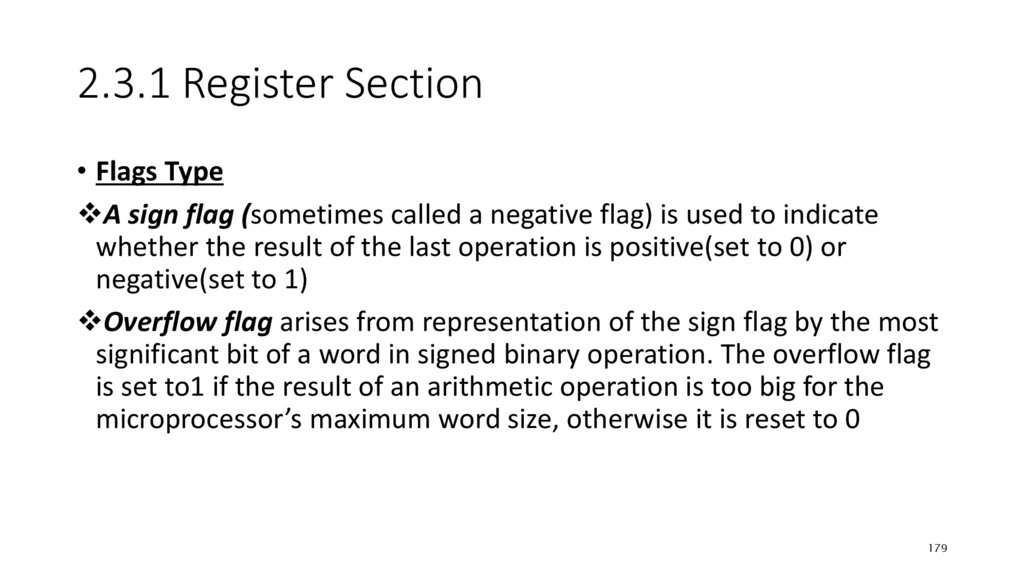
2.3.1 Register Section• Flags Type
A sign flag (sometimes called a negative flag) is used to indicate
whether the result of the last operation is positive(set to 0) or
negative(set to 1)
Overflow flag arises from representation of the sign flag by the most
significant bit of a word in signed binary operation. The overflow flag
is set to1 if the result of an arithmetic operation is too big for the
microprocessor’s maximum word size, otherwise it is reset to 0
179
180.
2.3.1 Register Section• EXAMPLE :
• Find the sign,carry,zero,overflow,and parity even flag for the following
arithmetic sign number:
(11110000)+(10100001) =10010001
SF =1 ,CF=1 ,ZF=0 ,OF=0 ,PF=0
180
181.
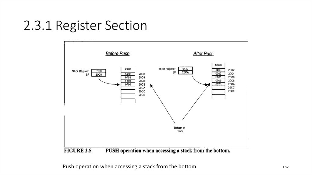
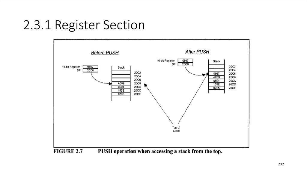
2.3.1 Register Section• Stack Pointer Register A stack consists of a number of RAM locations
set aside for reading data from or writing data into these locations
and is typically used by subroutines
• Two instructions, PUSH and POP, are usually available with a stack.
The PUSH operation
is defined as writing to the top or bottom of the stack, whereas the
POP operation means reading from the top or bottom of the stack.
181
182.
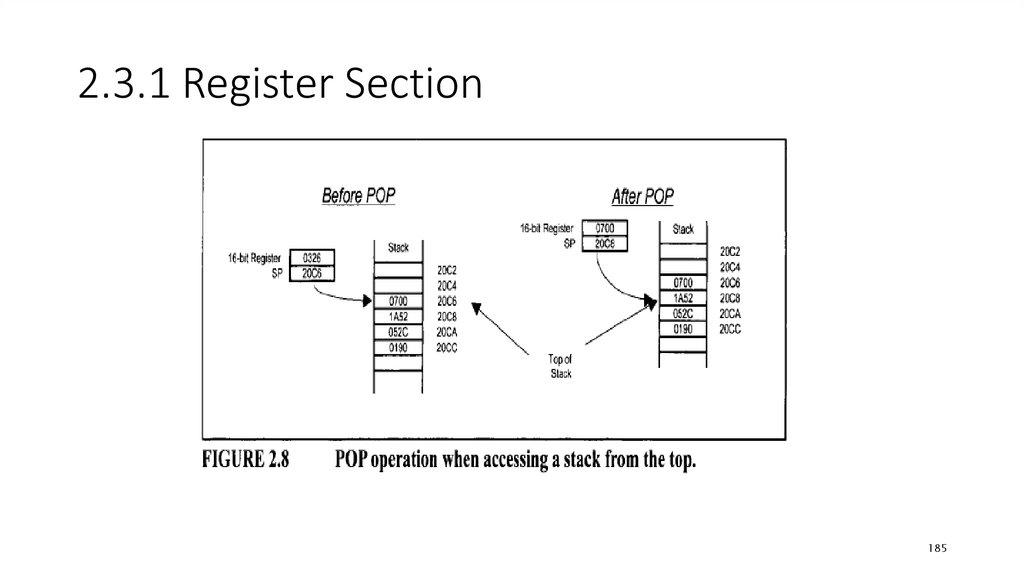
2.3.1 Register SectionPush operation when accessing a stack from the bottom
182
183.
2.3.1 Register Section183
184.
2.3.1 Register Section184
185.
2.3.1 Register Section185
186.
2.3.2 Control Unit• The main purpose of the control unit is to read and decode
instructions from the program memory.
• To execute an instruction, the control unit steps through the
appropriate blocks of the ALU based on the op-codes contained in the
instruction register.
186
187.
2.3.2 Control UnitControl Signal Actions
• RESET. This input is common to all microprocessors. When this input
pin is driven HIGH or LOW (depending on the microprocessor), the
program counter is loaded with a predefined address specified by the
manufacturer.
187
188.
2.3.2 Control UnitControl Signal Actions
• READ/WRITE (R/W) This output line is common to all
microprocessors. The status of this line tells the other
microcomputer elements whether the microprocessor is
performing a READ or a WRITE operation. A HIGH signal
on this line indicates a READ operation, and a LOW
indicates a WRITE operation.
188
189.
2.3.2 Control UnitControl Signal Actions
• READY, This is an input to a microprocessor. Slow devices (memory
and I/O) use this signal to gain extra time to transfer data to or
receive data from a microprocessor. The READY signal is usually an
active low signal; that is, LOW indicates that the microprocessor is
ready. Therefore, when the microprocessor selects a slow device,
the device places a LOW on the READY pin. The microprocessor
responds by suspending all its internal operations and enters a WAIT
state. When the device is ready to send or receive data, it removes
the READY signal. The microprocessor comes out of the WAIT state
and performs the appropriate operation.
189
190.
2.3.2 Control UnitControl Signal Actions
• Interrupt Request (INT or IRQ). The external I/O devices can
interrupt the microprocessor via this input pin on the microprocessor
chip. When this signal is activated by the external devices, the
microprocessor jumps to a special program called the interrupt service
routine. This program is normally written by the user for performing
tasks that the interrupting device wants the microprocessor to carry
out. After completing this program, the microprocessor returns to the
main program it was executing when the interrupt occurred.
190
191.
2.3.3 Arithmetic-Logic Unit• The ALU performs all the data manipulations, such as arithmetic and
logic operations, inside a microprocessor. The size of the ALU
conforms to the word length of the microcomputer.
• ALU Functions:
1.Binary addition and logic operations
2. Finding the one’s complement of data
3. Shifting or rotating the contents of a general-purpose register 1 bit to the left or
right through a carry
191
192.
2.3.4 Functional Representations ofSimple and Typical Microprocessors
• Simple Microprocessor
192
193.
2.3.4 Functional Representations ofSimple and Typical Microprocessors
• Buffer Register : Stores any data read from memory for further
processing by the ALU.
193
194.
2.3.4 Functional Representations ofSimple and Typical Microprocessors
• Typical Microprocessor
194
195.
195196.
• The Pentium contains two instruction pipelines: the U-pipe and the Vpipe. The U-pipe can execute all integer and floating-pointinstructions. The V-pipe can execute simple integer instructions
• The Pentium contains two separate cache memories: code cache and
data cache.
196
197.
2.3.5 Simplified Explanation of ControlUnit design
• The control unit performs two basic operations:
1. instruction interpretation
2. and instruction sequencing.
197
198.
2.3.5 Simplified Explanation of ControlUnit design
• There are two methods for designing a control unit:
hardwired control
Microprogrammed control(firmware)
clocked sequential circuit.
ROM inside the control unit (control
memory)
more expensive
flexibility
198
199.
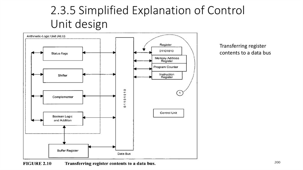
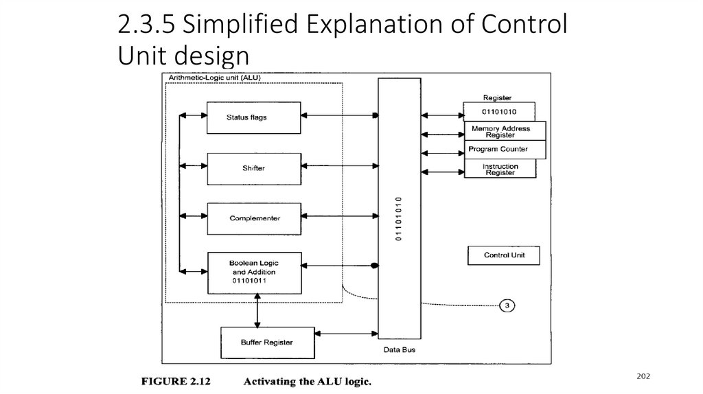
2.3.5 Simplified Explanation of ControlUnit design
• How incrementing the contents of the register by 1 is done in
microprogramming
control ??
(see figures in next slides)
199
200.
2.3.5 Simplified Explanation of ControlUnit design
Transferring register
contents to a data bus
200
201.
2.3.5 Simplified Explanation of ControlUnit design
201
202.
2.3.5 Simplified Explanation of ControlUnit design
202
203.
2.3.5 Simplified Explanation of ControlUnit design
203
204.
2.3.5 Simplified Explanation of ControlUnit design
204
205.
2.4 Program Execution by ConventionalMicroprocessors
• The following three steps for completing the instruction:
1.Fetch. The microprocessor fetches (instruction read) the instruction from the main memory
(external to the microprocessor) into the instruction register.
2. Decode. The microprocessor decodes or translates the instruction using the control unit. The
control unit inputs the contents of the instruction register, and then decodes (translates) the
instruction to determine the instruction type.
3. Execute. The microprocessor executes the instruction using the control unit. To accomplish the
task, the control unit generates a number of enable signals required by the instruction.
205
206.
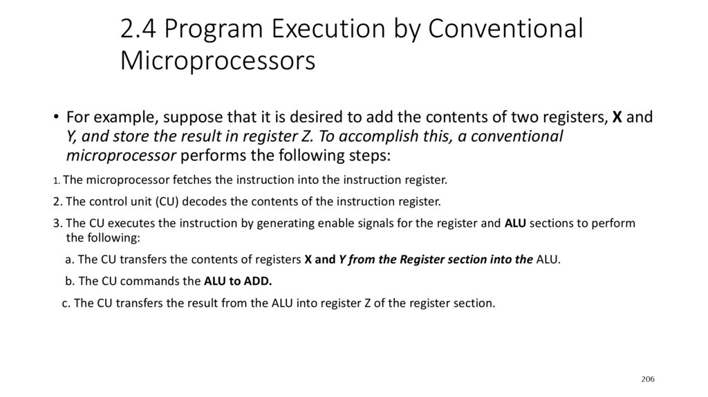
2.4 Program Execution by ConventionalMicroprocessors
• For example, suppose that it is desired to add the contents of two registers, X and
Y, and store the result in register Z. To accomplish this, a conventional
microprocessor performs the following steps:
1. The microprocessor fetches
the instruction into the instruction register.
2. The control unit (CU) decodes the contents of the instruction register.
3. The CU executes the instruction by generating enable signals for the register and ALU sections to perform
the following:
a. The CU transfers the contents of registers X and Y from the Register section into the ALU.
b. The CU commands the ALU to ADD.
c. The CU transfers the result from the ALU into register Z of the register section.
206
207.
2.5 Program Execution by typical 32-bitMicroprocessors
• Enhancement in 32-bit microprocessors (like Pentium) include : cache
memory, memory
management, pipelining, floating-point arithmetic, and branch
prediction.
• Cache memory is a high-speed read/write memory implemented as
on-chip
hardware in typical 32-bit microprocessors in order to increase
processing rates. This topic
is covered in more detail in Chapter 3.
207
208.
2.5 Program Execution by typical 32-bitMicroprocessors
• Memory management allows programmers to write programs much
larger than those that could fit in the main memory space available to
the microprocessors; the programs are simply stored on a secondary
device, such as a hard disk. This topic is covered in more detail in
Chapter 3.
208
209.
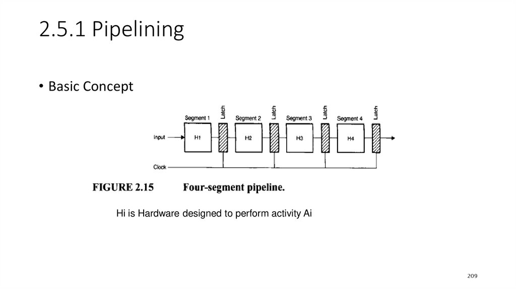
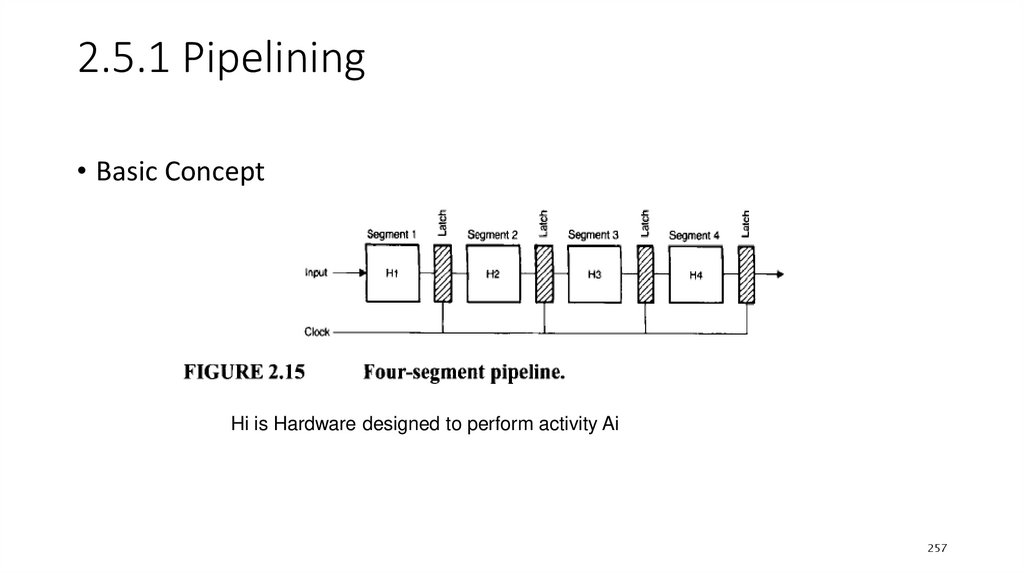
2.5.1 Pipelining• Basic Concept
Hi is Hardware designed to perform activity Ai
209
210.
2.5.1 Pipelining210
211.
2.5.1 Pipelining• Two Kind of Pipelining:
Arithmetic operations and instruction execution.
211
212.
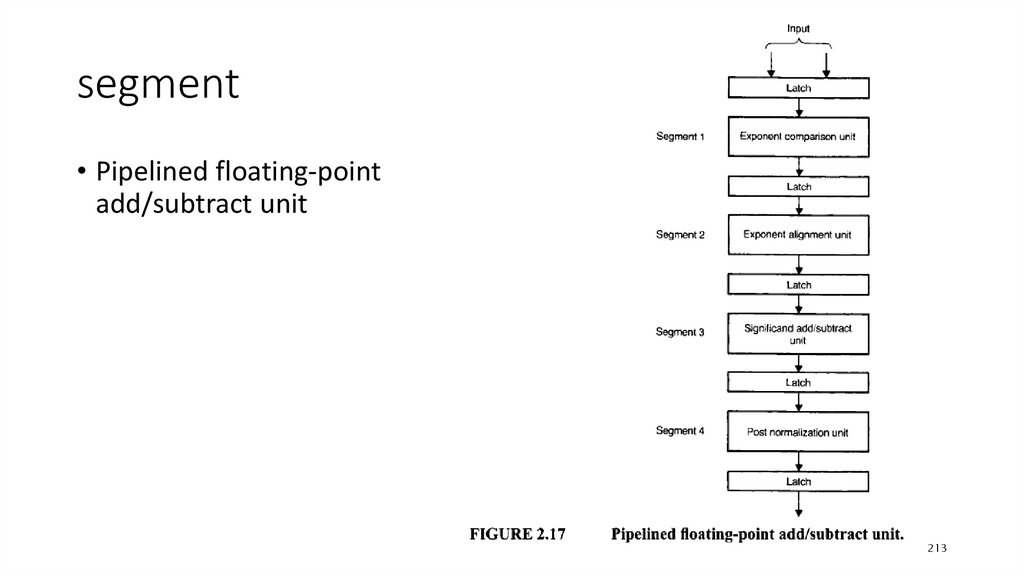
2.5.1 Pipelining• Arithmetic Pipelines
• Consider the process of adding two floating-point numbers x =0.9234
* 104 and y = 0.48 * 10 2.
First: exponents of x and y are unequal.
Second: exponent alignment.
Third: Perform the addition
Fourth: Normalize the final answer
212
213.
segment• Pipelined floating-point
add/subtract unit
213
214.
2.5.1 Pipelining• Instruction Pipelines
Instruction cycle typically involves the
following activities:
• 1. Instruction fetch - needs five clocks to complete
• 2. Instruction decode
• 3. Operand fetch (Data Read)
• 4. Operation execution
• 5. Result routing.
214
215.
Five-segmentinstruction pipeline
215
216.
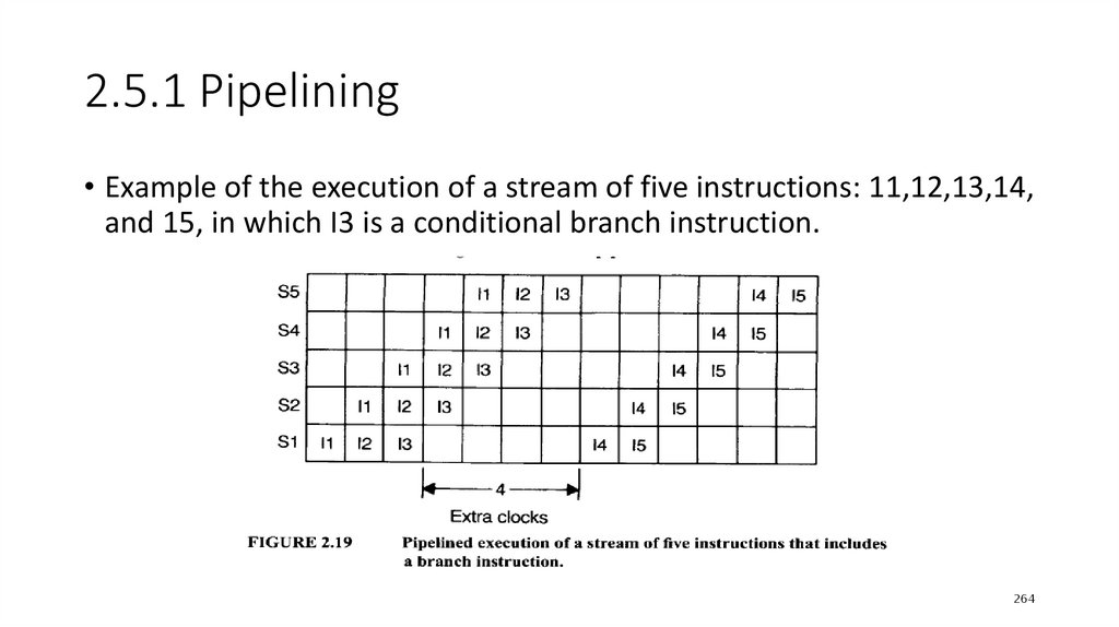
2.5.1 Pipelining• Example of the execution of a stream of five instructions: 11,12,13,14,
and 15, in which I3 is a conditional branch instruction.
216
217.
2.5.2 Branch Prediction Feature• This allows these microprocessors to anticipate jumps of the
instruction flow ahead of time.
217
218.
2.5.2 Branch Prediction Feature• To accomplish this, the Pentium includes on-chip
hardware called the Branch Unit (BU). The BU contains
the branch execution unit (BEU) and the branch
prediction unit (BPU). Whenever the Pentium
encounters a conditional branch instruction, it sends it
to the BU for execution. The BU evaluates the
instruction’s branch condition using the BEU and
determines whether the branch should or should not be
taken. Once the BU determines the branch condition, it
calculates the starting address (Branch target) of the
next block of code to be executed. The Pentium then
starts fetching code at the new address.
218
219.
2.6 Scalar and Superscalar Microprocessors• Scalar processors such as the 80486 can execute one instruction per
cycle.
The 80486 contains only one pipeline.
• Superscalar microprocessors, can execute
more than one instruction per cycle. These microprocessors contain
more than one pipeline.
• The Pentium, a superscalar microprocessor, contains two
independent pipelines. This
allows the Pentium to execute two instructions per cycle.
219
220.
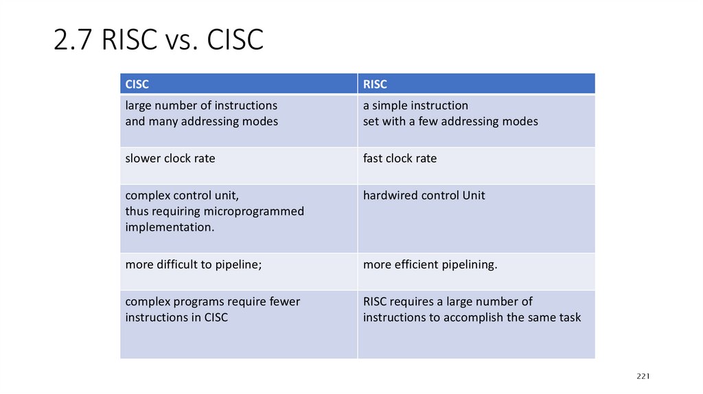
2.7 RISC vs. CISC• There are two types of microprocessor architectures:
RISC and CISC.
• RISC stand for (reduced instruction set computer) and
CISC for (complex instruction set computer)
220
221.
2.7 RISC vs. CISCCISC
RISC
large number of instructions
and many addressing modes
a simple instruction
set with a few addressing modes
slower clock rate
fast clock rate
complex control unit,
thus requiring microprogrammed
implementation.
hardwired control Unit
more difficult to pipeline;
more efficient pipelining.
complex programs require fewer
instructions in CISC
RISC requires a large number of
instructions to accomplish the same task
221
222.
2.7 RISC vs. CISC• Intel’s original Pentium is a CISC microprocessor. Intel Pentium Pro
and other succeeding members of the Pentium family and Motorola
68060 use a combination of RISC and CISC architectures for providing
high performance. The Pentium Pro and other succeeding
222
223.
LECTURE 11-12224.
Lecture 10-11MICROCOMPUTER ARCHITECTURE
Memory
ADC and DAC
224
225.
Outline• ADC and DAC
• 1.1 Basic Blocks of a Microcomputer
• 1.2 Typical Microcomputer Architecture
• 1.3 Single-Chip Microprocessor
• 1.4 Program Execution by Conventional Microprocessors
• 1.5 Program Execution by typical 32-bit Microprocessors
• 1.6 Scalar and Superscalar Microprocessors
• 1.7 RISC vs. CISC
225
226.
2.3.1 Register Section• Flags Type
A zero flag is used to show whether the result of an operation is
zero. It is set to1 if the result is zero, and it is reset to 0 if the result is
nonzero.
A parity flag is set to 1 to indicate whether the result of the last
operation contains either an even number of 1’s (even parity) or an
odd number of 1’s (odd parity), depending on the microprocessor.
226
227.
2.3.1 Register Section• Flags Type
A sign flag (sometimes called a negative flag) is used to indicate
whether the result of the last operation is positive(set to 0) or
negative(set to 1)
Overflow flag arises from representation of the sign flag by the most
significant bit of a word in signed binary operation. The overflow flag
is set to1 if the result of an arithmetic operation is too big for the
microprocessor’s maximum word size, otherwise it is reset to 0
227
228.
2.3.1 Register Section• EXAMPLE :
• Find the sign,carry,zero,overflow,and parity even flag for the following
arithmetic sign number:
(11110000)+(10100001) =10010001
SF =1 ,CF=1 ,ZF=0 ,OF=0 ,PF=0
228
229.
2.3.1 Register Section• Stack Pointer Register A stack consists of a number of RAM locations
set aside for reading data from or writing data into these locations
and is typically used by subroutines
• Two instructions, PUSH and POP, are usually available with a stack.
The PUSH operation
is defined as writing to the top or bottom of the stack, whereas the
POP operation means reading from the top or bottom of the stack.
229
230.
2.3.1 Register Section230
231.
2.3.1 Register Section231
232.
2.3.1 Register Section232
233.
2.3.1 Register Section233
234.
2.3.2 Control Unit• The main purpose of the control unit is to read and decode
instructions from the program memory.
• To execute an instruction, the control unit steps through the
appropriate blocks of the ALU based on the op-codes contained in the
instruction register.
234
235.
2.3.2 Control UnitControl Signal Actions
• RESET. This input is common to all microprocessors. When this input
pin is driven HIGH or LOW (depending on the microprocessor), the
program counter is loaded with a predefined address specified by the
manufacturer.
235
236.
2.3.2 Control UnitControl Signal Actions
• READ/WRITE (R/W) This output line is common to all
microprocessors. The status of this line tells the other
microcomputer elements whether the microprocessor is
performing a READ or a WRITE operation. A HIGH signal
on this line indicates a READ operation, and a LOW
indicates a WRITE operation.
236
237.
2.3.2 Control UnitControl Signal Actions
• READY, This is an input to a microprocessor. Slow devices (memory
and I/O) use this signal to gain extra time to transfer data to or
receive data from a microprocessor. The READY signal is usually an
active low signal; that is, LOW indicates that the microprocessor is
ready. Therefore, when the microprocessor selects a slow device,
the device places a LOW on the READY pin. The microprocessor
responds by suspending all its internal operations and enters a WAIT
state. When the device is ready to send or receive data, it removes
the READY signal. The microprocessor comes out of the WAIT state
and performs the appropriate operation.
237
238.
2.3.2 Control UnitControl Signal Actions
• Interrupt Request (INT or IRQ). The external I/O devices can
interrupt the microprocessor via this input pin on the microprocessor
chip. When this signal is activated by the external devices, the
microprocessor jumps to a special program called the interrupt service
routine. This program is normally written by the user for performing
tasks that the interrupting device wants the microprocessor to carry
out. After completing this program, the microprocessor returns to the
main program it was executing when the interrupt occurred.
238
239.
2.3.3 Arithmetic-Logic Unit• The ALU performs all the data manipulations, such as arithmetic and
logic operations, inside a microprocessor. The size of the ALU
conforms to the word length of the microcomputer.
• ALU Functions:
1.Binary addition and logic operations
2. Finding the one’s complement of data
3. Shifting or rotating the contents of a general-purpose register 1 bit to the left or
right through a carry
239
240.
2.3.4 Functional Representations ofSimple and Typical Microprocessors
• Simple Microprocessor
240
241.
2.3.4 Functional Representations ofSimple and Typical Microprocessors
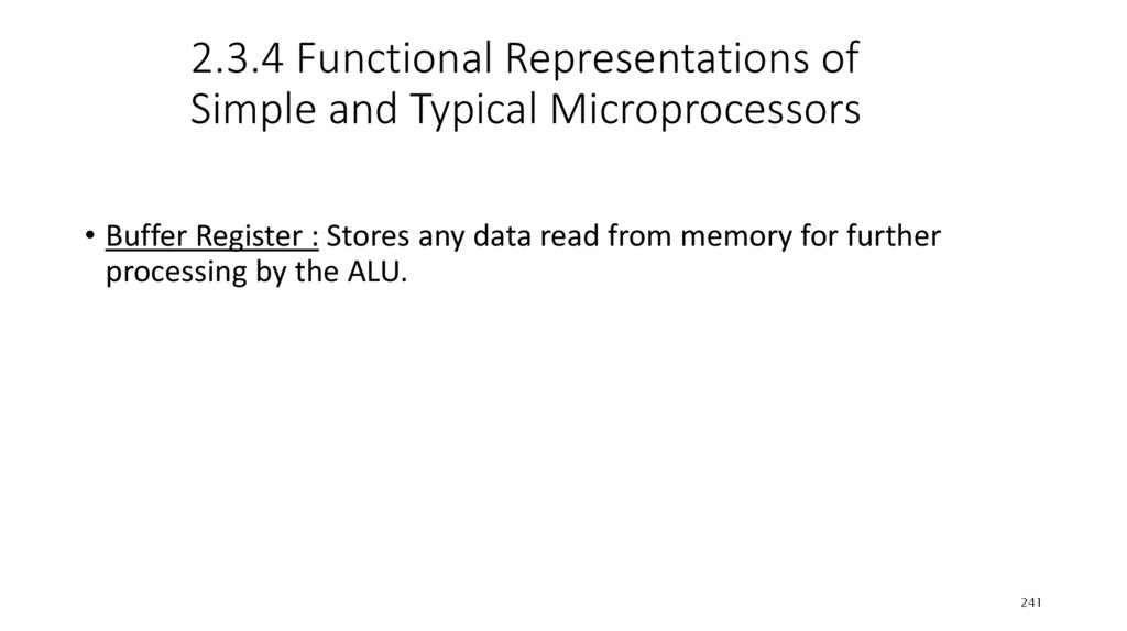
• Buffer Register : Stores any data read from memory for further
processing by the ALU.
241
242.
2.3.4 Functional Representations ofSimple and Typical Microprocessors
• Typical Microprocessor
242
243.
243244.
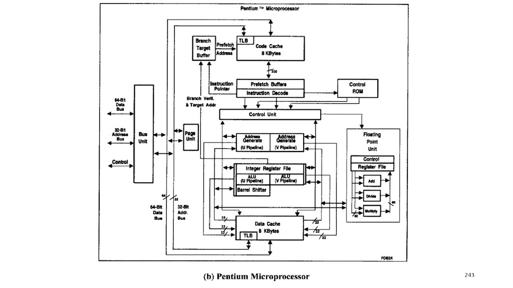
• The Pentium contains two instruction pipelines: the U-pipe and the Vpipe. The U-pipe can execute all integer and floating-pointinstructions. The V-pipe can execute simple integer instructions
• The Pentium contains two separate cache memories: code cache and
data cache.
244
245.
2.3.5 Simplified Explanation of ControlUnit design
• The control unit performs two basic operations:
1. instruction interpretation
2. and instruction sequencing.
245
246.
2.3.5 Simplified Explanation of ControlUnit design
• There are two methods for designing a control unit:
hardwired control
Microprogrammed control(firmware)
clocked sequential circuit.
ROM inside the control unit (control
memory)
more expensive
flexibility
246
247.
2.3.5 Simplified Explanation of ControlUnit design
• How incrementing the contents of the register by 1 is done in
microprogramming
control ??
(see figures in next slides)
247
248.
2.3.5 Simplified Explanation of ControlUnit design
248
249.
2.3.5 Simplified Explanation of ControlUnit design
249
250.
2.3.5 Simplified Explanation of ControlUnit design
250
251.
2.3.5 Simplified Explanation of ControlUnit design
251
252.
2.3.5 Simplified Explanation of ControlUnit design
252
253.
2.4 Program Execution by ConventionalMicroprocessors
• The following three steps for completing the instruction:
1.Fetch. The microprocessor fetches (instruction read) the instruction from the main memory
(external to the microprocessor) into the instruction register.
2. Decode. The microprocessor decodes or translates the instruction using the control unit. The
control unit inputs the contents of the instruction register, and then decodes (translates) the
instruction to determine the instruction type.
3. Execute. The microprocessor executes the instruction using the control unit. To accomplish the
task, the control unit generates a number of enable signals required by the instruction.
253
254.
2.4 Program Execution by ConventionalMicroprocessors
• For example, suppose that it is desired to add the contents of two registers, X and
Y, and store the result in register Z. To accomplish this, a conventional
microprocessor performs the following steps:
1. The microprocessor fetches
the instruction into the instruction register.
2. The control unit (CU) decodes the contents of the instruction register.
3. The CU executes the instruction by generating enable signals for the register and ALU sections to perform
the following:
a. The CU transfers the contents of registers X and Y from the Register section into the ALU.
b. The CU commands the ALU to ADD.
c. The CU transfers the result from the ALU into register Z of the register section.
254
255.
2.5 Program Execution by typical 32-bitMicroprocessors
• Enhancement in 32-bit microprocessors (like Pentium) include : cache
memory, memory
management, pipelining, floating-point arithmetic, and branch
prediction.
• Cache memory is a high-speed read/write memory implemented as
on-chip
hardware in typical 32-bit microprocessors in order to increase
processing rates. This topic
is covered in more detail in Chapter 3.
255
256.
2.5 Program Execution by typical 32-bitMicroprocessors
• Memory management allows programmers to write programs much
larger than those that could fit in the main memory space available to
the microprocessors; the programs are simply stored on a secondary
device, such as a hard disk. This topic is covered in more detail in
Chapter 3.
256
257.
2.5.1 Pipelining• Basic Concept
Hi is Hardware designed to perform activity Ai
257
258.
2.5.1 Pipelining258
259.
2.5.1 Pipelining• Two Kind of Pipelining:
Arithmetic operations and instruction execution.
259
260.
2.5.1 Pipelining• Arithmetic Pipelines
• Consider the process of adding two floating-point numbers x =0.9234
* 104 and y = 0.48 * 10 2.
First: exponents of x and y are unequal.
Second: exponent alignment.
Third: Perform the addition
Fourth: Normalize the final answer
260
261.
261262.
2.5.1 Pipelining• Instruction Pipelines
Instruction cycle typically involves the
following activities:
• 1. Instruction fetch - needs five clocks to complete
• 2. Instruction decode
• 3. Operand fetch (Data Read)
• 4. Operation execution
• 5. Result routing.
262
263.
263264.
2.5.1 Pipelining• Example of the execution of a stream of five instructions: 11,12,13,14,
and 15, in which I3 is a conditional branch instruction.
264
265.
2.5.2 Branch Prediction Feature• This allows these microprocessors to anticipate jumps of the
instruction flow ahead of time.
265
266.
2.5.2 Branch Prediction Feature• To accomplish this, the Pentium includes on-chip
hardware called the Branch Unit (BU). The BU contains
the branch execution unit (BEU) and the branch
prediction unit (BPU). Whenever the Pentium
encounters a conditional branch instruction, it sends it
to the BU for execution. The BU evaluates the
instruction’s branch condition using the BEU and
determines whether the branch should or should not be
taken. Once the BU determines the branch condition, it
calculates the starting address (Branch target) of the
next block of code to be executed. The Pentium then
starts fetching code at the new address.
266
267.
2.6 Scalar and Superscalar Microprocessors• Scalar processors such as the 80486 can execute one instruction per
cycle.
The 80486 contains only one pipeline.
• Superscalar microprocessors, can execute
more than one instruction per cycle. These microprocessors contain
more than one pipeline.
• The Pentium, a superscalar microprocessor, contains two
independent pipelines. This
allows the Pentium to execute two instructions per cycle.
267
268.
2.7 RISC vs. CISC• There are two types of microprocessor architectures:
RISC and CISC.
• RISC stand for (reduced instruction set computer) and
CISC for (complex instruction set computer)
268
269.
2.7 RISC vs. CISCCISC
RISC
large number of instructions
and many addressing modes
a simple instruction
set with a few addressing modes
slower clock rate
fast clock rate
complex control unit,
thus requiring microprogrammed
implementation.
hardwired control Unit
more difficult to pipeline;
more efficient pipelining.
complex programs require fewer
instructions in CISC
RISC requires a large number of
instructions to accomplish the same task
269
270.
2.7 RISC vs. CISC• Intel’s original Pentium is a CISC microprocessor. Intel Pentium Pro
and other succeeding members of the Pentium family and Motorola
68060 use a combination of RISC and CISC architectures for providing
high performance. The Pentium Pro and other succeeding
270
271.
LECTURE 12272.
273.
274.
275.
276.
277.
• The Requirements of a memory chipA memory chip requires address lines to identity a memory register.
The number of address lines required is determined by thenumber of registers in a
chip(2n = number of registers where n is the number of addresslines).A memory chip
requires a Chip Select (CS) signal to enablethe chip. The remaining address lines of
themicroprocessor can be connected to the CS signalthrough an interfacing logic.The
address lines connected to CS select the chip, and theaddress lines connected to the
address lines of the memorychip select the register.° The control signal Read (RD) enables
the output buffer,and data from the selected register are made available onthe output
lines.° The control signal (WR) enables the input buffer, and dataon the input lines are
written into memory cells.
278.
279.
• INPUT AND OUTPUT (I/O) DEVICES :• Input/output devices are the means through which theMPU communicates with "the outside world.“
• There are two different methods by which I/O devices canbe identified.1. I/Os with 8-Bit Addresses (PeripheralMapped I/O)
• The steps in communicating with an I/O deviceThe MPU places an 8-bit address on the address bus.which is decoded
by external decode logic.The MPU sends a control signal (I/O Read or I/O Write)and enables the I/O device.Data are
transferred using the data bus.2. I/Os with l6-Bit Addresses (Memory-Mapped I/O)the MPU uses 16 address lines to
identify an I/O device.This is known as memory-mapped I/O.
280.
281.
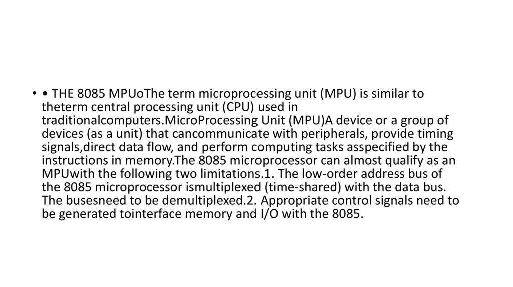
• • THE 8085 MPUoThe term microprocessing unit (MPU) is similar totheterm central processing unit (CPU) used in
traditionalcomputers.MicroProcessing Unit (MPU)A device or a group of
devices (as a unit) that cancommunicate with peripherals, provide timing
signals,direct data flow, and perform computing tasks asspecified by the
instructions in memory.The 8085 microprocessor can almost qualify as an
MPUwith the following two limitations.1. The low-order address bus of
the 8085 microprocessor ismultiplexed (time-shared) with the data bus.
The busesneed to be demultiplexed.2. Appropriate control signals need to
be generated tointerface memory and I/O with the 8085.
282.
283.
• • THE 8085 AND ITS PIN DESCRIPTION• The 8085 is an 8-bit generalpurpose microprocessorthat can address 64K Byte of memory.• It
has 40 pins and uses +5V for power. It can run at amaximum
frequency of 3 MHz.• The pins on the chip can be grouped into 6
groups:Address Bus and Multiplexed Data Bus. ( 16 Pins )Control and
Status Signals. ( 6 Pins )Power supply and frequency. ( 4 Pins
)Externally Initiated Signals. ( 7 Pins )Interupt Signals. ( 5 pins )Serial
I/O ports. ( 2 Pins )
284.
8085 Microprocessor Pin Out Diagram285.
286.
287.
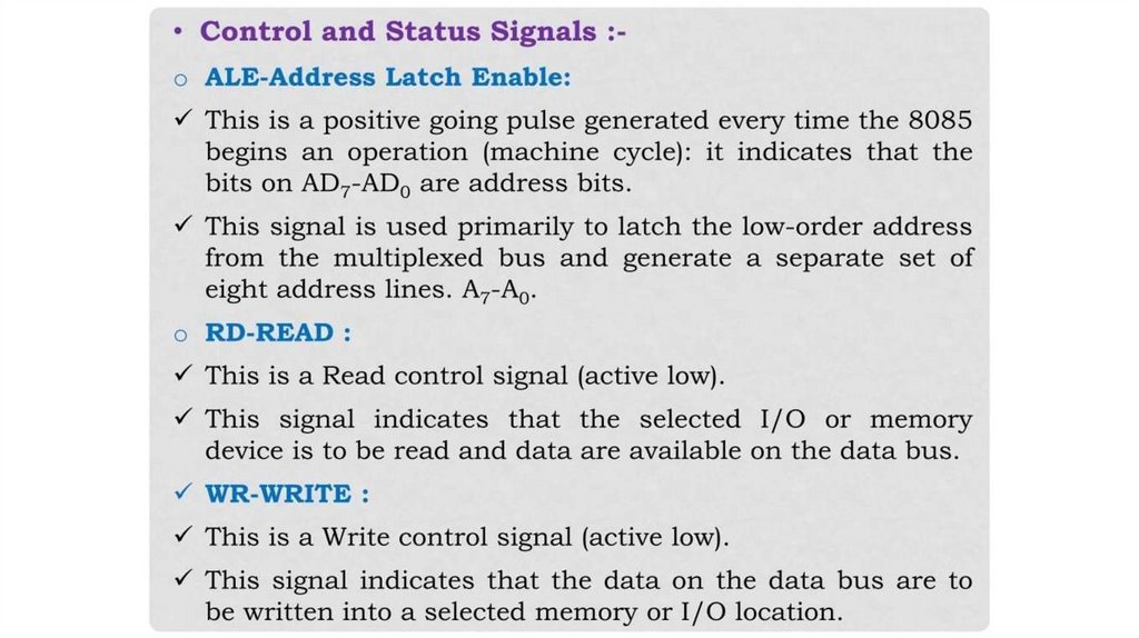
• • Control and Status Signals :-o ALE-Address Latch Enable:This is a positivegoing pulse generated every time the 8085begins an operation (machine
cycle): it indicates that thebits on AD7-AD, are address bits.This signal is
used primarily to latch the low-order addressfrom the multiplexed bus
and generate a separate set ofeight address lines. A7-A0-o RD-READ :This
is a Read control signal (active low).This signal indicates that the selected
I/O or memorydevice is to be read and data are available on the data
bus.WR-WRITE :This is a Write control signal (active low).This signal
indicates that the data on the data bus are tobe written into a selected
memory or I/O location.
288.
289.
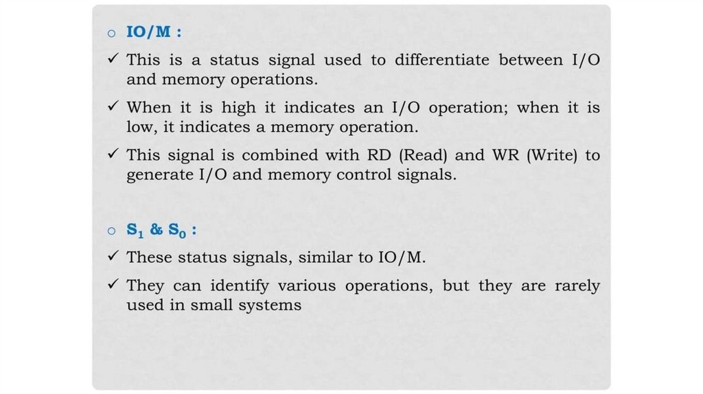
• IO/M :This is a status signal used to differentiate between I/Oandmemory operations.When it is high it indicates an I/O operation;
when it islow, it indicates a memory operation.This signal is
combined with RD (Read) and WR (Write) togenerate I/O and
memory control signals.o S, & So :These status signals, similar to
IO/M.They can identify various operations, but they are rarelyused in
small systems
290.
291.
292.
• • Interrupts :Processor has 5 interrupts. They are presented belowinthe order of their priority (from lowest to highest):INTR is maskable
interrupt. When the interrupt occursthe processor fetches
instruction from the bus.RST 5.5 is a maskable interrupt. When this
interrupt is… received the processor saves the contents of the PC
cregister into stack and branches to 2CH (hexadecimal)address.RST
6.5 is a maskable interrupt. When this interrupt isreceived the
processor saves the contents of the PCregister into stack and
branches to 34H (hexadecimal)address.
293.
294.
• RST 7.5 is a maskable interrupt. When this interrupt isreceived theprocessor saves the contents of the PCregister into stack and
branches to 3CH (hexadecimal)address.TRAP is a non-maskable
interrupt. When this interruptis received the processor saves the
contents of the PCregister into stack and branches to 24H
(hexadecimal)address.All maskable interrupts can be enabled or
disabled usingEI and DI instructions.
295.
296.
297.
298.
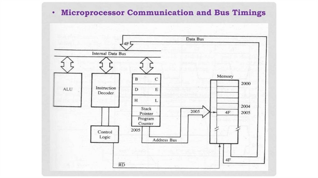
• TIMING SIGNALS FOR FETCHING AN INSTRUCTIONAt T1 , the high order 8address bits (20H) are placed on>the address lines A8 - A15 and the low
order bits areplaced on AD7-ADO.The ALE signal goes high to indicate that
AD0 - AD8 arecarrying an address.At exactly the same time, the IO/M
signal goes low toindicate a memory operation.At the beginning of the T2
cycle, the low order 8 addressbits are removed from AD7- ADO and the
controllersends the Read (RD) signal to the memory.The signal remains
low (active) for two clock periods toallow for slow devices.During T2 ,
memory places the data from the memory>location on the lines AD7- AD0
.
299.
300.
• During T3 the RD signal is Disabled (goes high). This turnsoff theoutput Tri-state buffers in the memory. That makesthe AD7- ADO
lines go to high impedence mode.The machine code or the byte
(4FH) is decoded by theinstruction decoder, and the contents of
theaccumulator are copied into register C. This task isperformed
during the period T4
301.
302.
• • DEMULTIPLEXING AD7-ADO• From the above description, it becomesobvious thatthe AD7- ADO lines are serving a dual purpose andthat they
need to be demultiplexed to get all theinformation.• The high order bits of
the address remain on the busfor three clock periods. However, the low
order bitsremain for only one clock period and they would belost if they
are not saved externally.• Also, notice that the low order bits of the
addressdisappear when they are needed most.• To make sure we have the
entire address for the fullthree clock cycles, we will use an external latch
tosave the value of AD7- ADO when it is carrying theaddress bits. We use
the ALE signal to enable thislatch.
303.
Demultiplexing AD7-AD0304.
• Given that ALE operates as a pulse during T1, wewill be able to latchthe address. Then when ALEgoes low, the address is saved and the
AD7- ADOlines can be used for their purpose as the bi-directional
data lines.
305.
306.
• • CYCLES AND STATES• From the above discussion, we can defineterms thatwill become handy later on:• T- State: One subdivision of
an operation. A T-statelasts for one clock period.• An instruction's
execution length is usuallymeasured in a number of T-states. (clock
cycles).• Machine Cycle: The time required to complete
oneoperationofaccessingmemory, I/O,oracknowledging an external
request.• This cycle may consist of 3 to 6 T-states.• Instruction Cycle:
The time required to complete theexecution of an instruction.• In
the 8085, an instruction cycle may consist of 1to 6 machine cycles.
307.
308.
• •GENERATING CONTROL SIGNALSThe 8085 generates a single RD
signal. However, thesignal needs
to be used with both memory and
I/O. So,it must be combined with
the IO/M signal to
generatedifferent control signals
for the memory and I/O.• Keeping
in mind the operation of the IO/M
signal wecan use the following
circuitry to generate the right
setof signals:
309.
310.
311.
• • THE 8085 MACHINE CYCLES• The 8085 executes several types ofinstructions witheach requiring a different number of operations
ofdifferent types. However, the operations can begrouped into a
small set.• The three main types are:• Memory Read and Write.• I/O
Read and Write.• Request Acknowledge.• These can be further
divided into various operations(machine cycles).
312.
313.
• • OPCODE FETCH MACHINE CYCLE• The first step of executing anyinstruction is theOpcode fetch cycle.• In this cycle, the
microprocessor brings in theinstruction's Opcode from memory.• To
differentiate this machine cycle from the verysimilar "memory read"
cycle, the control & statussignals are set as follows:• IO/M=0, s0 and
s1 are both 1.• This machine cycle has four T-states.• The 8085 uses
the first 3 T-states to fetch theopcode.• T4 is used to decode and
execute it.• It is also possible for an instruction to have 6 T-states in
an opcode fetch machine cycle.
314.
315.
316.
• the memory read machine cycle• To understand the memory readmachine cycle, let'sstudy the execution of the following instruction:
MVI A, 322000H3E• In memory, this instruction looks like:2001H32
The first byte 3EH represents the opcode forloading a byte into the
accumulator (MVI A), thesecond byte is the data to be loaded.• The
8085 needs to read these two bytes from memorybefore it can
execute the instruction. Therefore, it willneed at least two machine
cycles.• The first machine cycle is the opcode fetchdiscussed earlier.
The second machine cycle is the Memory ReadCycle.
317.
318.
• • MACHINE CYCLES VS. NUMBER OF BYTES INTHE INSTRUCTION• Machinecycles and instruction length, do not have a directrelationship.• To
illustrate lets look at the machine cycles needed to executethe following
instruction.• STA 2065H• This is a 3-byte instruction requiring 4 machine
cycles and 13 T-states.32H 2010-• The machine code will be stored65H
2011Hin memory as shown to the right20H2012H• This instruction
requires the following 4 machine cycles:• Opcode fetch to fetch the
opcode (32H) from location 2010H,decode it and determine that 2 more
bytes are needed (4 T-states).• Memory read to read the low order byte
of the address (65H) (3T-states).•• Memory read to read the high order
byte of the address (20H) (3T-states).• A• A memory write to write the
contents of the accumulator intothe memory location.
319.
LECTURE 13MICROPROCESSORS
320.
Microprocessors321.
322.
• Input / OutputInput DevicesSwitches , Keyboard , …OutputDevices:Seven Segments (LEDs) , printer , Monitor ,…The processor
reads the instructions from thememory , data from the input
devices,processes them, produces the output
323.
The CPU includes ALU, control Units, and Various Registers324.
The Von Neumann ModelIt uses von Neumann execution cycle
(also called the fetch-decode-execute cycle)
325.
326.
• A cycle could be as follows:The control unit fetches the nextprograminstruction from the memory, using the programcounter to
determine where the instruction islocated.The instruction is decoded
into a language theALU can understand.Any data operands required
to execute theinstruction are fetched from memory and placedinto
registers within the CPU.The ALU executes the instruction and places
theresults in registers or memory.
327.
328.
329.
330.
• Advances in SemiconductorTechnologyIC- Integrated Circuits -> fewtransistors and diodes onone chipSSI -small scale Integration-> few
gates on one chipMSI- Medium scale Integration- 100 gates on a
chipLSI - Large Scale Integration - 1000 gates on a chipVLSI - Very
large scale IntegrationSLSI - Super Large Scale IntegrationBorders
between VLSI and SLSI are not strict.
331.
Microprocessor programming* Machine language
Instruction written in binary
format
• Assembly language
Text based format add a, b
• *High level language
332.
Z80instruction
s and
alphanum
eric codes
333.
Microprocessor Based System334.
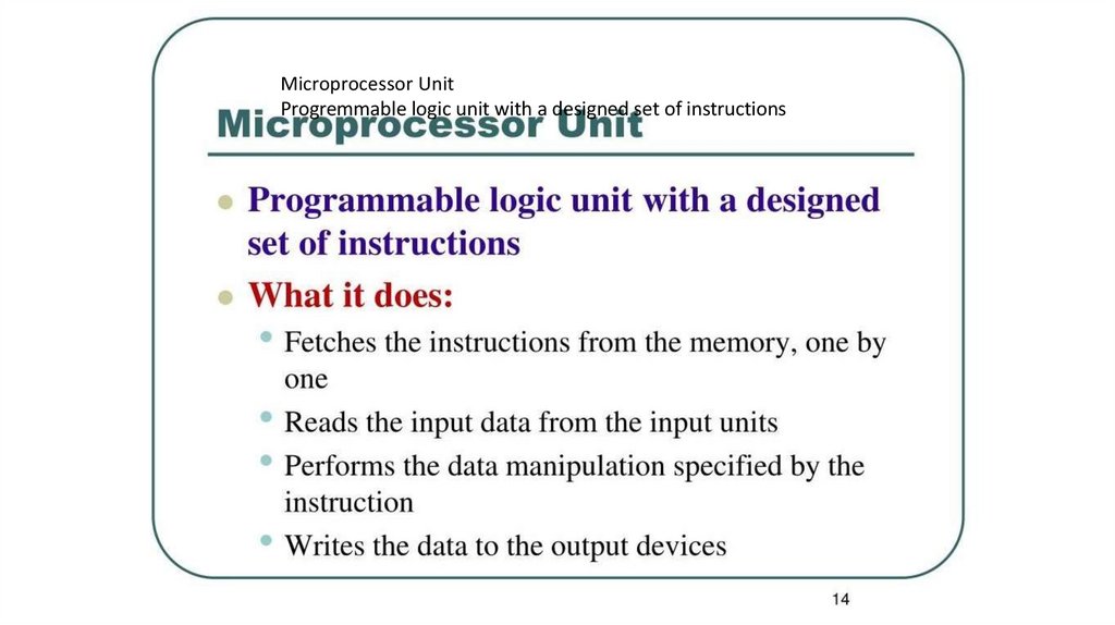
Microprocessor UnitProgremmable logic unit with a designed set of instructions
335.
MPU frequently communicates with the memory, I/O devices336.
What does it needs to do so..337.
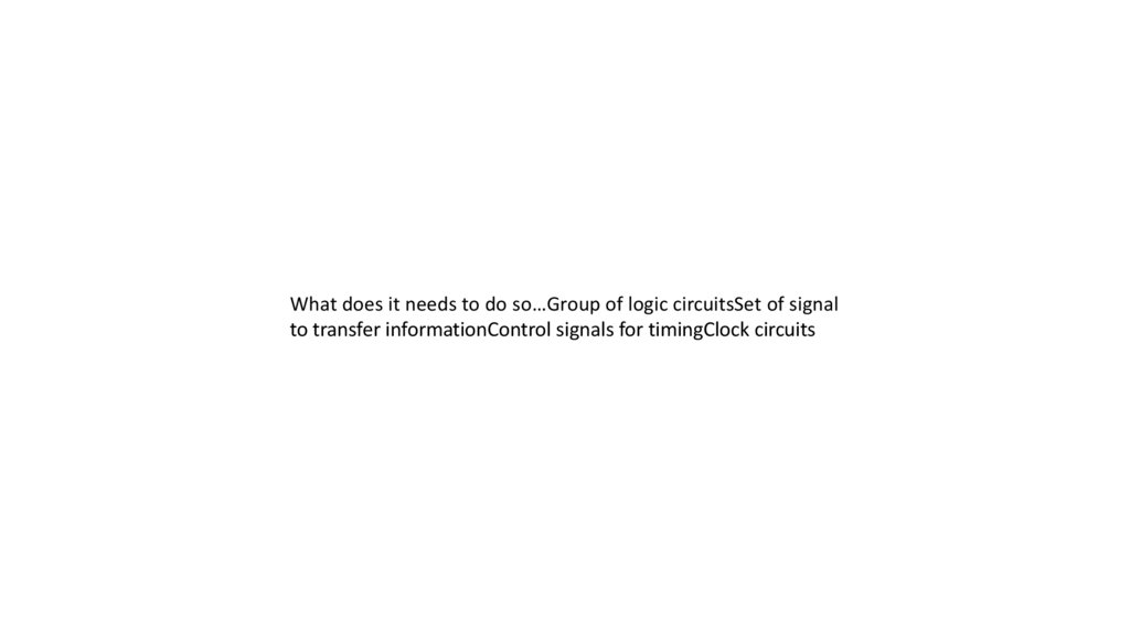
What does it needs to do so…Group of logic circuitsSet of signalto transfer informationControl signals for timingClock circuits
338.
339.
Program-initiated operationsand BusesanMicroprocessor andMemory OperationsMemory ReadReads instructions or data
from the memoryMemory WriteWrites instructions and data
into memoryI/O ReadAccepts data from input devicesI/O
WriteWrites data to output devices
340.
341.
Program-initiated operationsand BusesFrom where to read orto write?We need an address! Right?How the input/output will
know about the operation?We need a control signal to tell
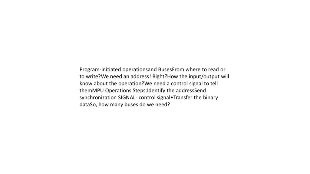
themMPU Operations Steps:Identify the addressSend
synchronization SIGNAL- control signal•Transfer the binary
dataSo, how many buses do we need?
342.
343.
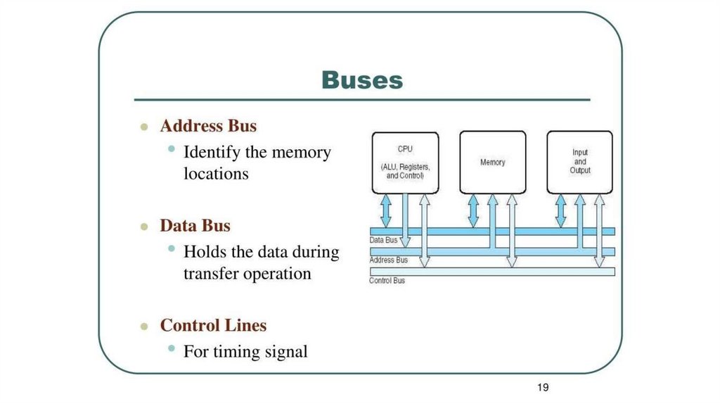
BusesAddress BusIdentify the memorylocationsCPU(ALU,Registers,and Control)MemoryInputandOutputData BusData
BusHolds the data duringAddress Bustransfer operationControl
BusControl Lines° For timing signal
344.
345.
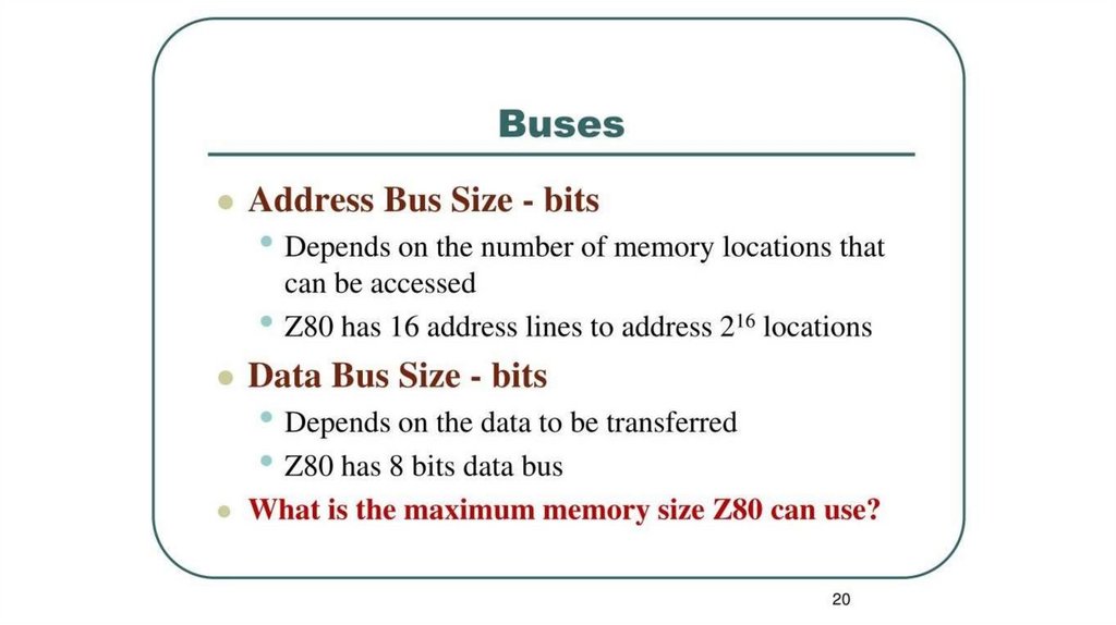
BusesAddress Bus Size - bitsDepends on the number ofmemory locations thatcan be accessedZ80 has 16 address lines
to address 216 locationsData Bus Size - bitsDepends on the
data to be transferredZ80 has 8 bits data busWhat is the
maximum memory size Z80 can use?
346.
347.
348.
349.
350.
351.
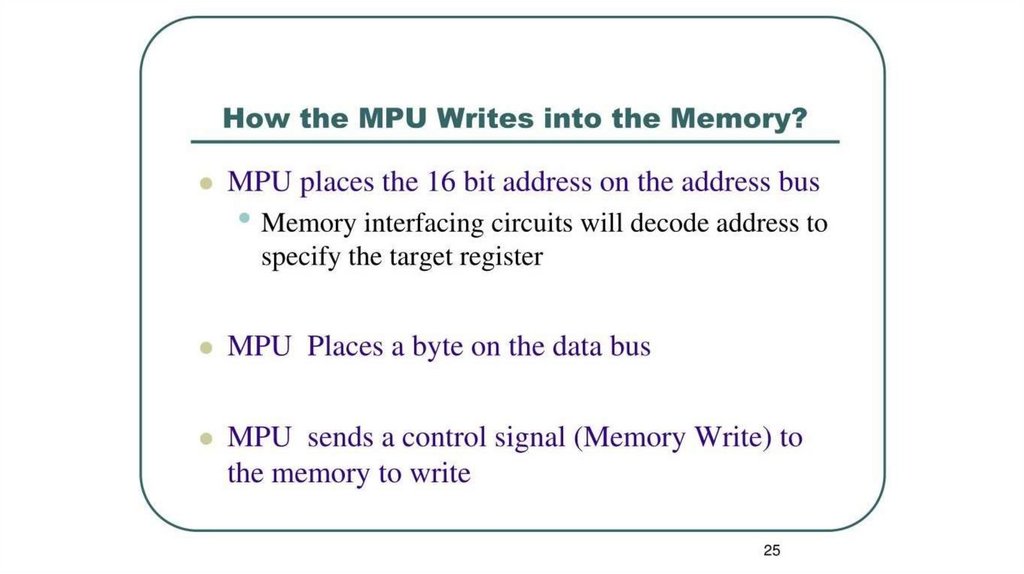
How the MPU Writes into the Memory?•MPU places the 16 bitaddress on the address busMemory interfacing circuits will
decode address tospecify the target registerMPU Places a byte
on the data bus• MPU sends a control signal (Memory Write)
tothe memory to write
352.
353.
How the MPU reads from the Memory?MPU places the 16 bitaddress on the address busMemory interfacing circuits will
decode address tospecify the target registerMPU sends a
control signal (Memory Read) tothe memory to enable the
output buffer•The memory puts the data on the data bus and
theprocessor will read it
354.
LECTURE 13MICROPROCESSOR
355.
356.
357.
358.
BusesAddress Bus Size - bitsDepends on the number ofmemory locations thatcan be accessedZ80 has 16 address lines
to address 216 locationsData Bus Size - bitsDepends on the
data to be transferredZ80 has 8 bits data bus• What is the
maximum memory size Z80 can use?
359.
360.
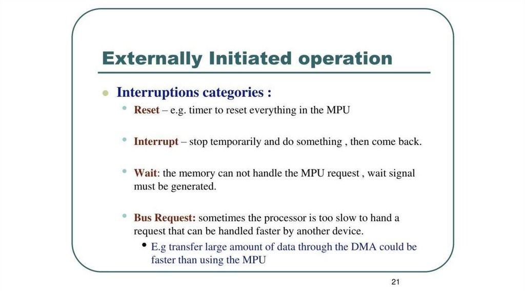
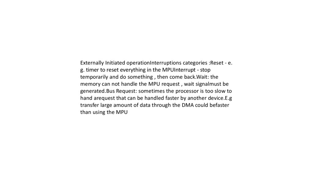
Externally Initiated operationInterruptions categories :Reset - e.g. timer to reset everything in the MPUInterrupt - stop
temporarily and do something , then come back.Wait: the
memory can not handle the MPU request , wait signalmust be
generated.Bus Request: sometimes the processor is too slow to
hand arequest that can be handled faster by another device.E.g
transfer large amount of data through the DMA could befaster
than using the MPU
361.
362.
363.
364.
365.
366.
LECTURE 14367.
MicrocontrollersFundamentals of Logic Design
By Dana Utebayeva
368.
Micro-Controller• A single chip Computer (to some extent)
• Has CPU
1.
2.
3.
4.
RAM
EEPROM
I/O in form of pins
Peripherals (Timer , Communication
modes , ADC
etc)
369.
Background• Line Following Robots
• Wireless keyboards
• They were made using
Microcontrollers
370.
• Suppose we want to make a Line followingRobot
• What do we do ?
• Use a computerwith 2.4Ghz Intel core I7
with 4 Gb RAM , 500 Gb Hard disk , 1 Gb
Graphics Card ??
371.
Why not a Computer?• PC is a general purpose computer.
• Can run thousand of softwares
• Microsoft ppt in which you are seeing this
presentation
• Games (NFS , AOE , Call of Duty)
• Highly expensive
372.
Why MCU• Small reflected by the word “MICRO”
• Inexpensive
• Ideal for doing repetitive tasks
• Easy to use
• Highly Efficient and fast
373.
Selecting a MCU• Two family of MCU extremely popular
a) AVR
b) PIC
• We use AVR series of MCU from Atmel
• The instructions are fed once in the form of a
Hex file
374.
Tools Required -> CVAVR375.
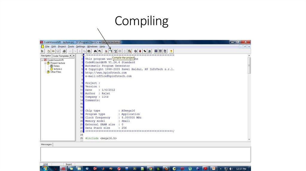
Compiler -> CVAVR• The code is written in C language so we need to convert
it into the format
that
Atmega understands
376.
Transfer code toAtmega AVR Studio377.
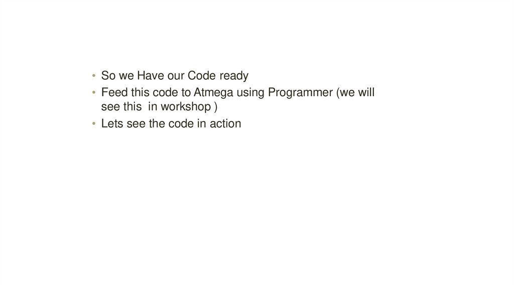
Avr Programmer378.
• So we need two softwares overalla) CVAVR –> Editor and Compiler
b) Avr Studio –>
Transfer Code
to Atmega
379.
Atmega 16380.
Basics of C language• If else block
• If(condition)
{
……
}
else
{
……
}
381.
While & For• While (conditon)
{
… ...
}
• for(initialisation; condition;
increment)
{
……
}
382.
383.
• Lets Begin byblinking a simple
LED
384.
Circuit Diagram385.
Getting Started withCVAVR386.
OpenCVAVR
Go to
File
New
Project
387.
Open CVAVR388.
Go to File389.
Click on New390.
Select Project- > ClickOK391.
Click YES392.
Select Chip393.
Introductionto I/O
394.
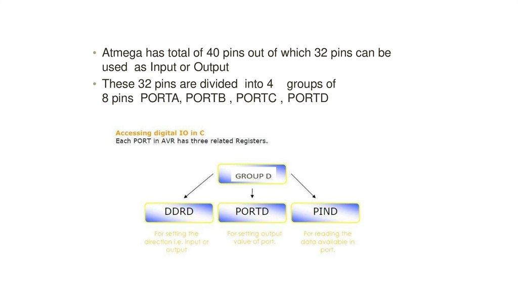
• Atmega has total of 40 pins out of which 32 pins can beused as Input or Output
• These 32 pins are divided into 4 groups of
8 pins PORTA, PORTB , PORTC , PORTD
395.
Data Direction register(DDR)• This sets direction for
all pins (32)
• Direction for these pins can be Input or Output
• To blink an LED we need to set pin as “OUTPUT” but
“HOW“ ?
• DDRA = 0b00000001 ;
• DDRA = 0x01 ;
• 1 Stands for Output & 0 stands for Input
396.
397.
What is Next ?• We have set the Pin as Output
• What else do we need to light the LED ??
• Supply of 5 Volts !!! This is given by PORT
Register
398.
PORT Register• Only after you have set the Pin to Output you can
control them through this Register
• It is a 8 bit register . It corresponds to the pin in same
manner as that of DDR Register
• Used to set output value ( 0 or 1 ) only if the
corresponding Pin has been set as output by DDR
Register
• PORTA= 0b 00000001;
or
• PORTA= 0x01 ;
• 1 stands for 5V
• 0 stands for 0V
MS
B
L
L
L
L
L
L
L
H
LS
B
399.
Simple QuestionsDDRA= 0b 00101100
DDRD = 0xf4
DDRC = 0b 01111110
DDRB = 0x3b
Assume all 32 pins set as
output
PORTA = 0b00001100;
PORTD = 0b11110000;
PORTB.4=1;
PORTC.2=1;
400.
Setting I/O401.
Go to Ports402.
• Click on In to make that pin Output• Can do so for all four ports
403.
Click on File404.
Generate Save and Exit405.
Enter name (3times)406.
Where is the code stored?407.
Then Click Save408.
Name of Project &Location409.
Writing the Code410.
• NOTE : We write our code in While block• While (1)
{
PORTA.1=1; // sets the Pin to 5
volts PORTA.1=0; // sets the Pin
to 0 volts
}
• This makes the LED to blink but we cannot see
blinking !!!
411.
• This is becauseAtmega runs at a frequency of
8000000 Hz
• We need to introduce delay so as to see blinking
• Use header file delay.h
•Function to be used delay_ms(time in
millis); While (1)
{
delay_ms(100
0);
PORTA.1=1;
delay_ms(100
0);
PORTA.1=0;
}
412.
How to compile• Code is written in C language but Atmega
understands Hex file
so we need to convert the C file to Hex file
413.
Compiling414.
Make the Project415.
Check for errors416.
HexFile• You can find the Hex file in Bin folder or the EXE
folder of the directory where You installed CVAVR
417.
• So we Have our Code ready• Feed this code to Atmega using Programmer (we will
see this in workshop )
• Lets see the code in action
418.
Lets add an Input• Most Common Input Button
Since we have already made A0 as Input
We connect a button to that pin
If button is pressed light the LED else turn it off
First draw the Circuit Diagram
419.
Circuit Diagram420.
• Never leave any Input pin unconnected /floating at any point of time while your circuit
is working
• In Last Circuit A0 is floating when button is not
pressed so our Circuit Diagram is wrong
421.
• What is the Voltage at the Floating PIN ?Not 5 V
Not 0V
Its UNDEFINED
So never leave an input pin unconnected
Use the Concept of Pull up / Pull down
422.
• In Laymanterms
• PULL DOWN : Gives 0V when unconnected
• PULL UP : Gives 5V when unconnected
• Connect the PIN to Ground through a resistance for
pulling down
• Connect the PIN to 5V through a resistance for Pulling
up
423.
Correct CircuitDiagram
424.
PIN Register• It is a 8 bit register . It corresponds to the pin in same
manner as that of DDR Register
• It is used to read voltage at a pin
• To be used only after the pin has been set as input by
DDR register
425.
Using Pin Registerint a; // Define the variable a to store the value of
voltage a=PINA.0; // read value at pin A.0 (make
sure it is input)
If (a==1) // if voltage is 5V
{
PORTA.1=1; // Light the LED
}
else
{
PORTA.1=0; // Turn off the LED
}
426.
Code in Action427.
1) What is a Microprocessor?• 2) What is Microcontroller?
• In simple words, The microprocessor is useful in very
intensive processes. It only contains a CPU (central processing
unit) but there are many other parts needed to work with the
CPU to complete a process. These all other parts are
connected externally.
• The microcontroller is designed for a specific task or to
perform the assigned task repeatedly. Once the program is
embedded on a microcontroller chip, it can’t be altered easily
and you may need some special tools to reburn it. As per
application, the process is fixed in microcontroller. Hence, the
output depends on the input given by the user or sensors or
predefined inputs.
• Microprocessors are not made for a specific task as well as
they are useful where tasks are complex and tricky like the
development of software, games, and other applications that
require high memory and where input and output are not
defined.
• Do you understand? I think a bit, but it's ok, let’s understand
by some daily life examples
• The applications easily connect with concepts, so let's find
out day to day life examples
• e.g. Calculator, Washing Machine, ATM machine, Robotic
Arm, Camera, Microwave oven, Oscilloscope, Digital
multimeter, ECG Machine, Printer so on and so forth.
Microprocessor
consists
of only aHome
Central Processing Unit, whereas Micro Controller contains a CPU,
• A) Household devices:
Complex home
security,
Memory,
I/O alland
integrated
one chip.
computers, Video game
systems
manyinto
more.
The microprocessor is useful in Personal Computers whereas Micro Controller is useful in an embedded
• B) Transportation and
Industrial Devices: Automobiles, trains,
system.
planes, Computer servers,
high tech medical
devices,
The microprocessor
uses an external
busetc.
to interface to RAM, ROM, and other peripherals, on the other
hand,
Microcontroller
usesare
an internal
controlling
bus.
• Did you notice! All the
above
applications
complex
and
Microprocessors
are data.
based on Von Neumann model Microcontrollers are based on Harvard architecture
they need to process
all complicated
The microprocessor is complicated and expensive, with a large number of instructions to process but
Microcontroller is inexpensive and straightforward with fewer instructions to process.
428.
LECTURE 15 APPLICATIONSOF MICROPROCESSORS
MICROCONTROLLERS
429.
Applications ofMicroprocessors &
Microcontrollers
Dana Utebayeva
430.
OutlinePC, LAPTOPS AND TOP MODELS OF
PROCESSORS
MOBILE PHONES
AI, MACHINE LEARNING AND DEEP
LEARNING, COMPUTER VISION
PROJECTS
431.
Best Processors of PCs and Laptops432.
Mobile Processor• The mobile processor is used in mobile computers
and cell phones. The CPU IC is designed for laptop
computers to run without a fan, with a power
rating of less than 10-15W, which is cool enough
without a fan.
433.
5 chips (in alphabetic order)especiallydesigned for AI
AMD Radeon Instinct
Usage
• Radeon Instinct is AMD’s brand of
deep learning oriented GPUs. It
replaced AMD’s FirePro S brand in
2016. Compared to the Radeon
brand of mainstream
consumer/gamer products, the
Radeon Instinct branded products
are intended to accelerate deep
learning, artificial neural network,
and high-performance
computing/GPGPU applications.
434.
Apple A11 BionicNeural Engine
• The Apple A11 Bionic is a 64-bit ARM-based system on
a chip (SoC), designed by Apple Inc. and manufactured
by TSMC. It first appeared in the iPhone 8, iPhone 8
Plus, and iPhone X. The A11 includes dedicated neural
network hardware that Apple calls a “Neural Engine”.
This neural network hardware can perform up to 600
billion operations per second and is used for Face ID,
Animoji and other machine learning tasks. The neural
engine allows Apple to implement neural network and
machine learning in a more energy-efficient manner
than using either the main CPU or the GPU.
435.
Google Tensor Processing Unit• A tensor processing unit (TPU) is an
application-specific integrated circuit
(ASIC) developed by Google
specifically for machine learning.
Compared to a graphics processing
unit, it is designed for a high volume of
low precision computation (e.g. as
little as 8-bit precision) with higher
IOPS per watt, and lacks hardware for
rasterisation/texture mapping. The
chip has been specifically designed
for Google’s TensorFlow framework.
However, Google still uses CPUs and
GPUs for other types of machine
learning. Other AI accelerator designs
are appearing from other vendors also
and are aimed at embedded and
robotics markets.
436.
Huawei Kirin970
• Kirin 970 is powered by an 8-core CPU
and a new generation 12-core GPU. Built
using a 10nm advanced process, the
chipset packs 5.5 billion transistors into
an area of only one cm². HUAWEI’s
flagship Kirin 970 is HUAWEI’s first
mobile AI computing platform featuring a
dedicated Neural Processing Unit (NPU).
Compared to a quad-core Cortex-A73
CPU cluster, the Kirin 970’s
heterogeneous computing architecture
delivers up to 25x the performance with
50x greater efficiency.
437.
IBM Power9• Recently launched by IBM,
Power9 is a chip which has a
new systems architecture that is
optimized for accelerators used
in machine learning. Intel makes
Xeon CPUs and Nervana
accelerators and NVIDIA makes
Tesla accelerators. IBM’s
Power9 is literally the Swiss
Army knife of ML acceleration
as it supports an astronomical
amount of IO and bandwidth,
10X of anything that’s out there
today
438.
Intel Nervana• The Nervana ‘Neural Network
Processor’ uses a parallel, clustered
computing approach and is built pretty
much like a normal GPU. It has 32 GB of
HBM2 memory dedicated in 4 different
8 GB HBM2 stacks, all of which is
connected to 12 processing clusters
which contain further cores (the exact
count is unknown at this point). Total
memory access speeds combine to a
whopping 8 terabits per second.
439.
Nvidia Tesla V100• NVIDIA® Tesla® V100 is the
world’s most advanced data
center GPU ever built to
accelerate AI, HPC, and
graphics. Powered by NVIDIA
Volta™, the latest GPU
architecture, Tesla V100 offers
the performance of 100 CPUs in
a single GPU—enabling data
scientists, researchers, and
engineers to tackle challenges
that were once impossible.