Похожие презентации:
Programmable Logic and FPGA
1. Programmable logic and FPGA
CPU ArchitectureSerge Karabchevsky
2. Objectives
What is a programmable logicWhat is an FPGA
Structure
Special functions
Comparison and Usages
Altera Cyclone II 20 FPGA
Design Flow
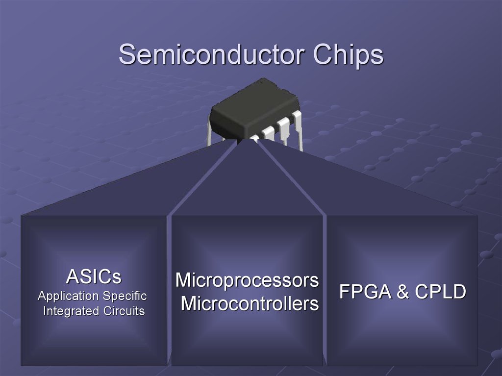
3. Semiconductor Chips
ASICsApplication Specific
Integrated Circuits
Microprocessors
FPGA & CPLD
Microcontrollers
4. Programmable logic
An integrated circuit that can beprogrammed/reprogrammed with a digital
logic of a curtain level.
Started at late 70s and constantly growing
Now available of up to approximately 700K
Flip-Flops in a single chip.
5. Advantages
Short Development timeReconfigurable
Saves board space
Flexible to changes
No need for ASIC expensive design and
production
Fast time to market
Bugs can be fixed easily
Of the shelf solutions are available
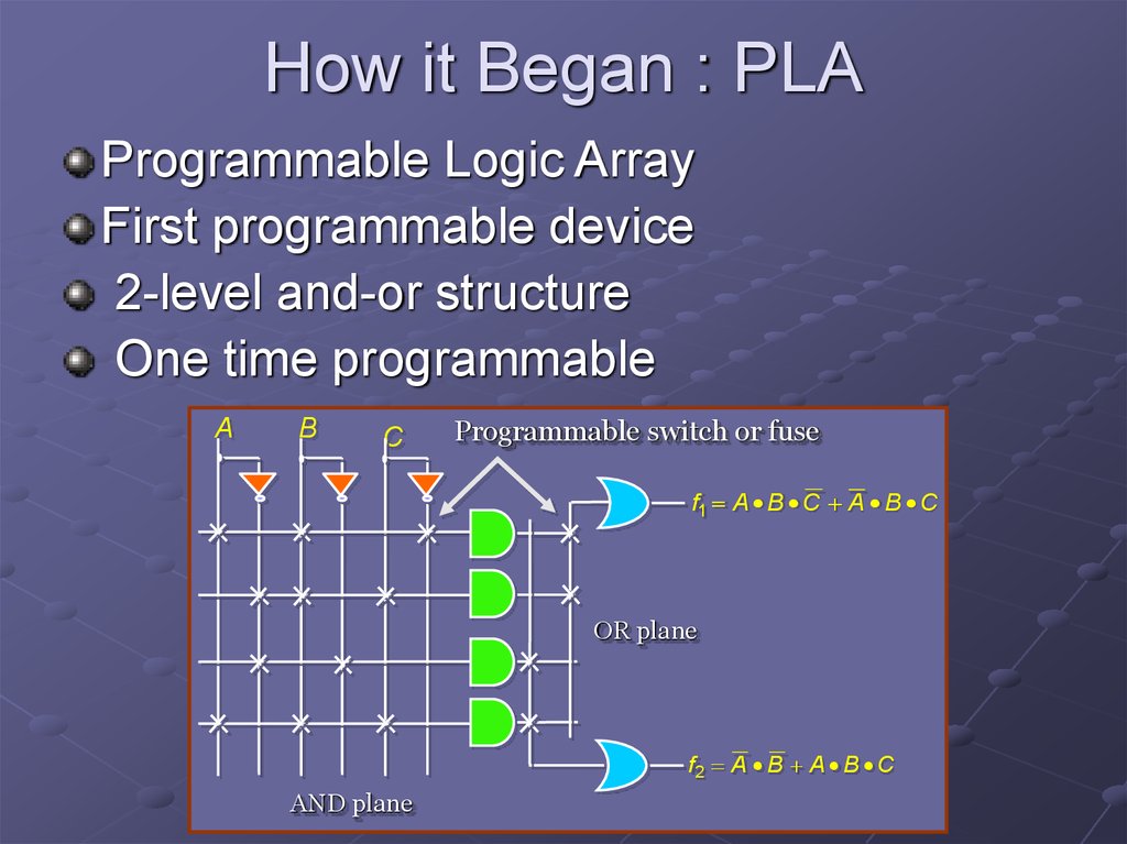
6. How it Began : PLA
Programmable Logic ArrayFirst programmable device
2-level and-or structure
One time programmable
A
B
C
Programmable switch or fuse
f1 A B C A B C
OR plane
f2 A B A B C
AND plane
7. SPLD - CPLD
Simple Programmable logic deviceSingle AND Level
Flip-Flops and feedbacks
Complex Programmable logic device
D
AND plane
Interconnection Matrix
MUX
I/O Block
Clock
Q
PLD
Block
Enable
f1
Flip-flop
PLD
Block
I/O Block
Select
C
I/O Block
B
I/O Block
A
Several PLDs Stacked together
PLD
Block
PLD
Block
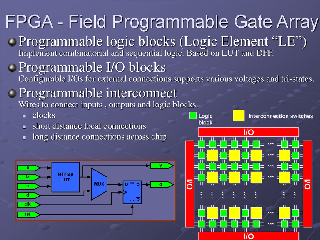
8. FPGA - Field Programmable Gate Array
Programmable logic blocks (Logic Element “LE”)Implement combinatorial and sequential logic. Based on LUT and DFF.
Programmable I/O blocks
Configurable I/Os for external connections supports various voltages and tri-states.
Programmable interconnect
Wires to connect inputs , outputs and logic blocks.
clocks
Logic
block
short distance local connections
long distance connections across chip
MUX
D
SET
Q
q
I/O
N Input
LUT
I/O
c
I/O
y
a
b
Interconnection switches
d
CLR
Q
clk
rst
I/O
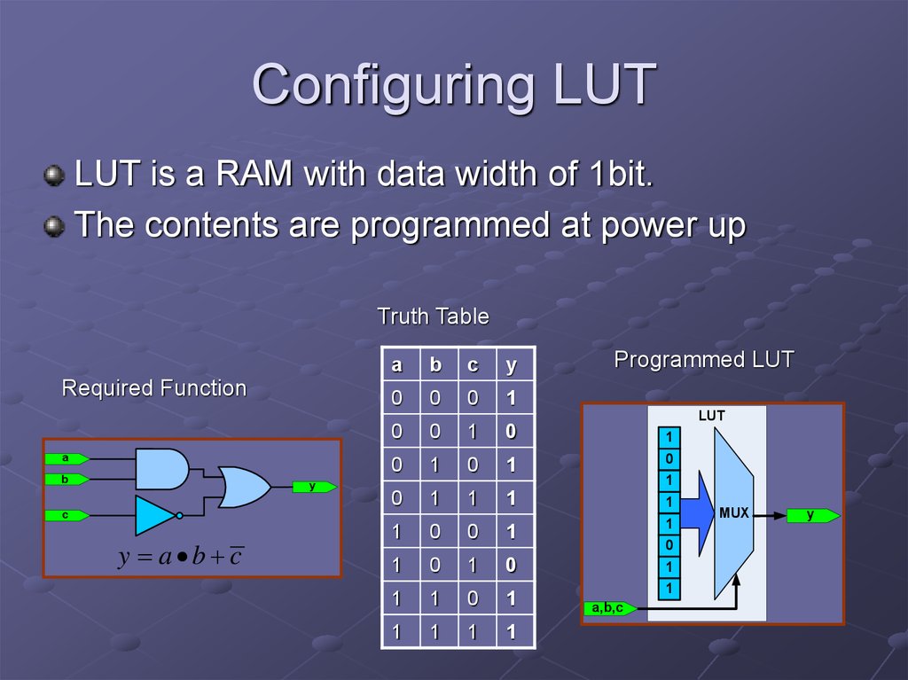
9. Configuring LUT
LUT is a RAM with data width of 1bit.The contents are programmed at power up
Truth Table
Required Function
Programmed LUT
a
b
c
y
0
0
0
1
0
0
1
0
1
0
1
0
1
0
0
1
1
1
1
LUT
a
b
y
1
c
y a b c
1
0
0
1
1
1
0
1
0
1
1
1
0
1
1
1
1
1
0
1
a,b,c
MUX
y
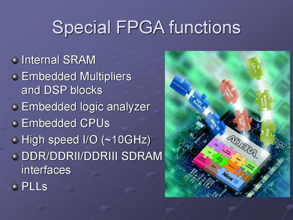
10. Special FPGA functions
Internal SRAMEmbedded Multipliers
and DSP blocks
Embedded logic analyzer
Embedded CPUs
High speed I/O (~10GHz)
DDR/DDRII/DDRIII SDRAM
interfaces
PLLs
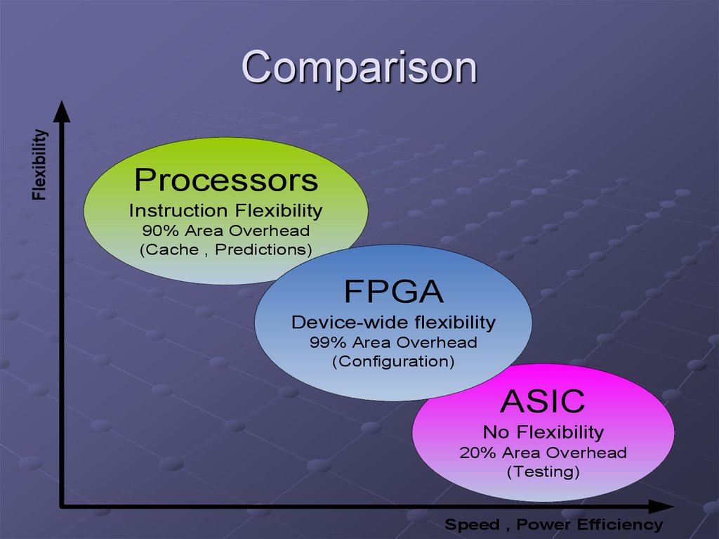
11. Comparison
FlexibilityComparison
Processors
Instruction Flexibility
90% Area Overhead
(Cache , Predictions)
FPGA
Device-wide flexibility
99% Area Overhead
(Configuration)
ASIC
No Flexibility
20% Area Overhead
(Testing)
Speed , Power Efficiency
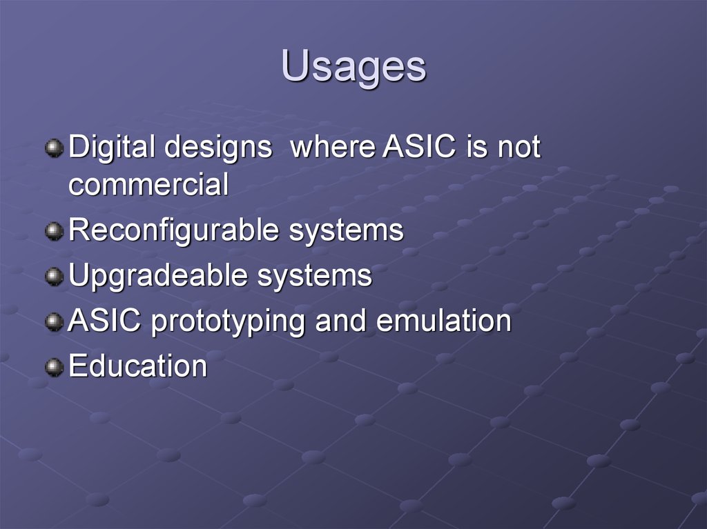
12. Usages
Digital designs where ASIC is notcommercial
Reconfigurable systems
Upgradeable systems
ASIC prototyping and emulation
Education
13. Manufacturers
XilinxAltera
Lattice
Actel
We will work with Altera FPGAs
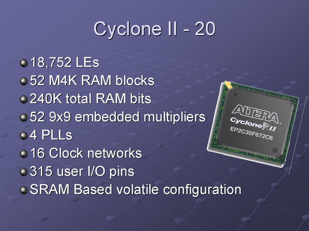
14. Cyclone II - 20
18,752 LEs52 M4K RAM blocks
240K total RAM bits
52 9x9 embedded multipliers
4 PLLs
16 Clock networks
315 user I/O pins
SRAM Based volatile configuration
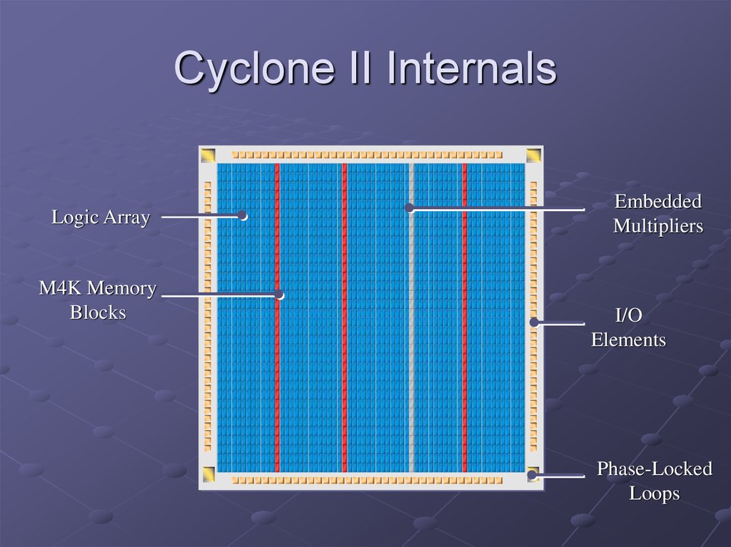
15. Cyclone II Internals
Logic ArrayM4K Memory
Blocks
Embedded
Multipliers
I/O
Elements
Phase-Locked
Loops
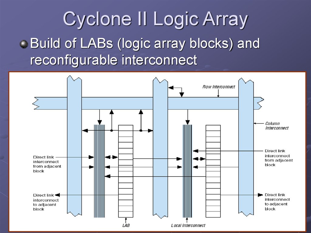
16. Cyclone II Logic Array
Build of LABs (logic array blocks) andreconfigurable interconnect
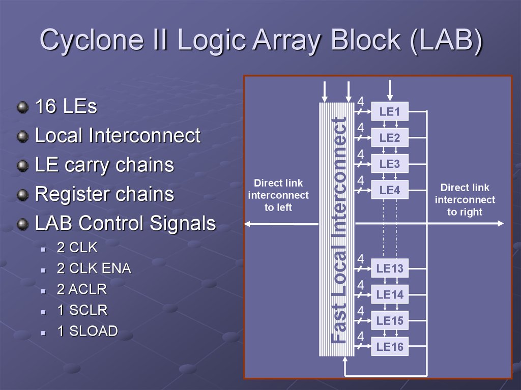
17. Cyclone II Logic Array Block (LAB)
2 CLK2 CLK ENA
2 ACLR
1 SCLR
1 SLOAD
4
Direct link
interconnect
to left
Fast Local Interconnect
16 LEs
Local Interconnect
LE carry chains
Register chains
LAB Control Signals
4
4
4
4
4
4
4
LE1
LE2
LE3
LE4
LE13
LE14
LE15
LE16
Direct link
interconnect
to right
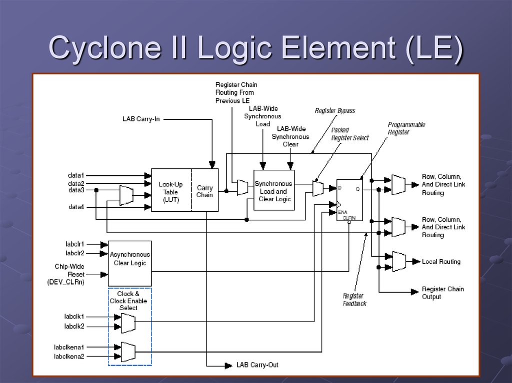
18. Cyclone II Logic Element (LE)
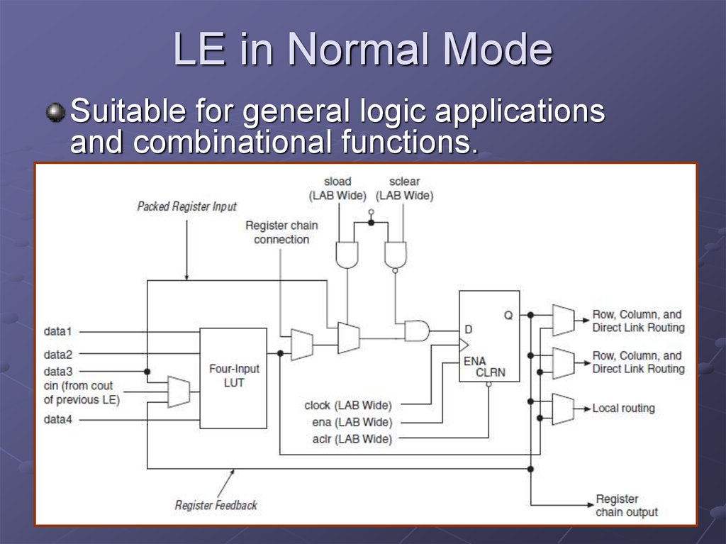
19. LE in Normal Mode
Suitable for general logic applicationsand combinational functions.
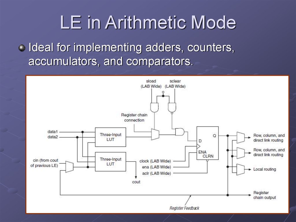
20. LE in Arithmetic Mode
Ideal for implementing adders, counters,accumulators, and comparators.
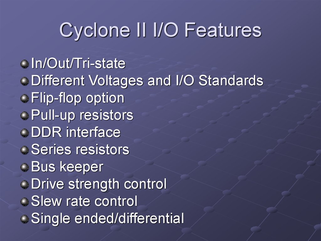
21. Cyclone II I/O Features
In/Out/Tri-stateDifferent Voltages and I/O Standards
Flip-flop option
Pull-up resistors
DDR interface
Series resistors
Bus keeper
Drive strength control
Slew rate control
Single ended/differential
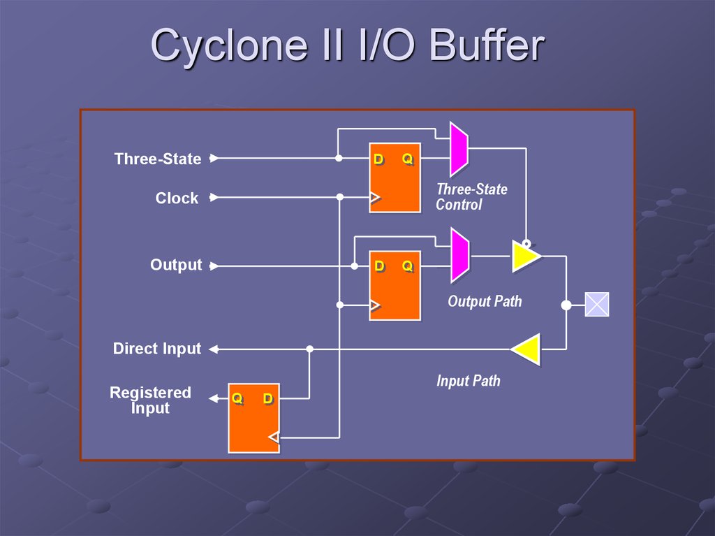
22. Cyclone II I/O Buffer
Three-StateD
Q
Three-State
Control
Clock
Output
D
Q
Output Path
Direct Input
Registered
Input
Input Path
Q
D
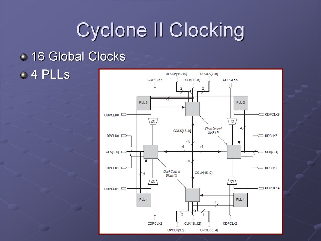
23. Cyclone II Clocking
16 Global Clocks4 PLLs
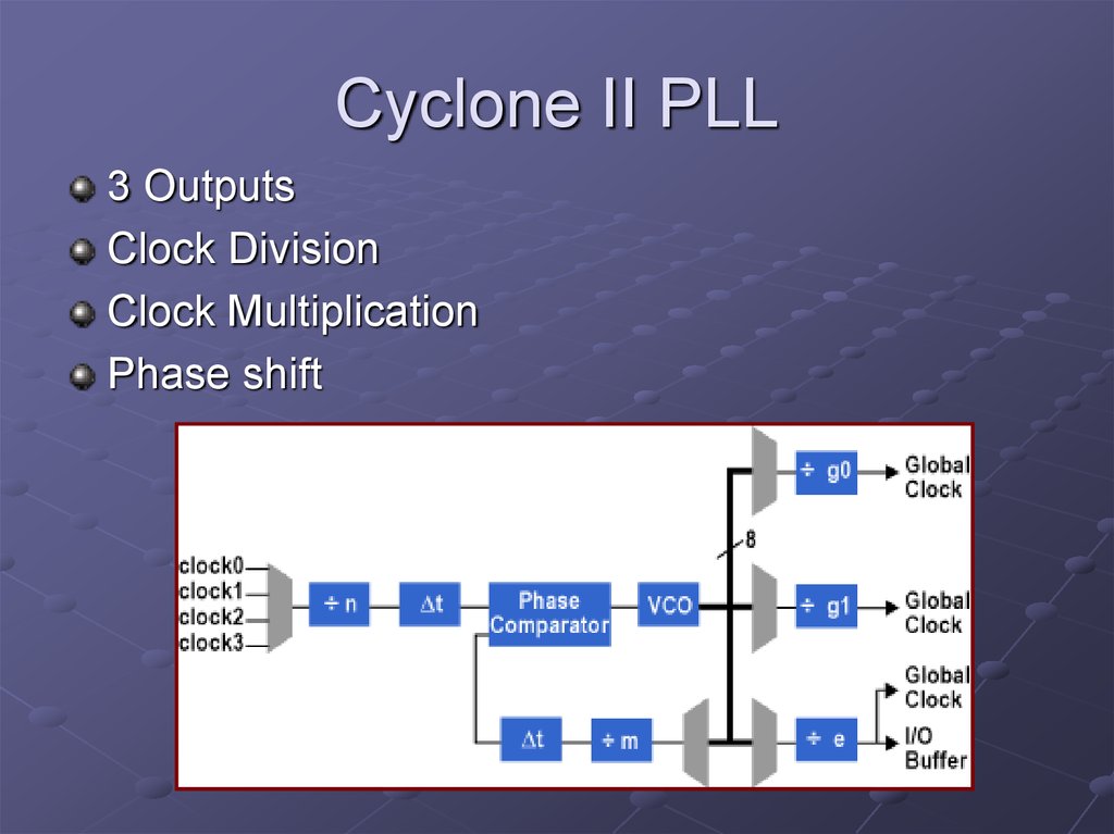
24. Cyclone II PLL
3 OutputsClock Division
Clock Multiplication
Phase shift
25. Memory
True Dual port RAM/ROM with dual clockVariable data width
4K×1, 2K×2, 1K×4, 512×8, 512×9, 256×16, 256×18
128×32, 128×36 (not available in true dual-port mode)
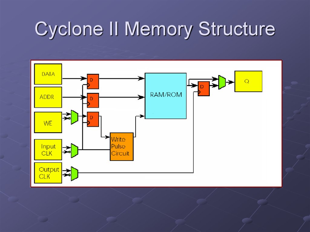
Input data and address are registered
1 Clock Write latency
Output data can be registered
Read latency of 1 or 2 clocks
Byte Enable
26. Cyclone II Memory Structure
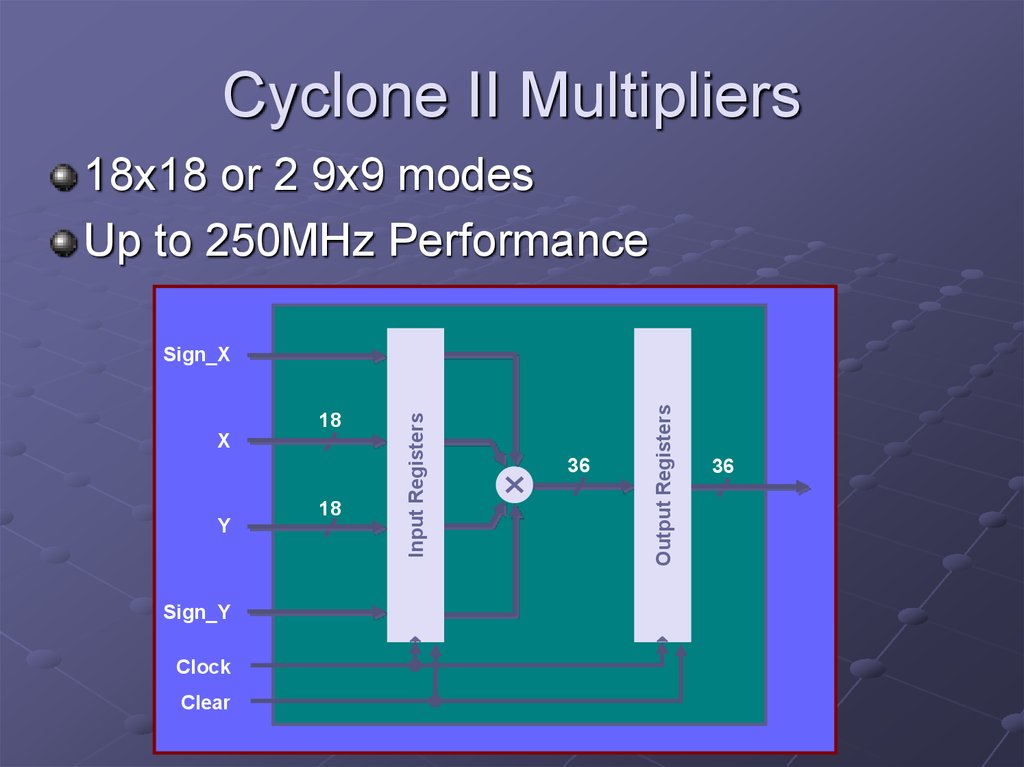
27. Cyclone II Multipliers
18x18 or 2 9x9 modesUp to 250MHz Performance
Y
Sign_Y
Clock
Clear
18
36
Output Registers
18
X
Input Registers
Sign_X
36
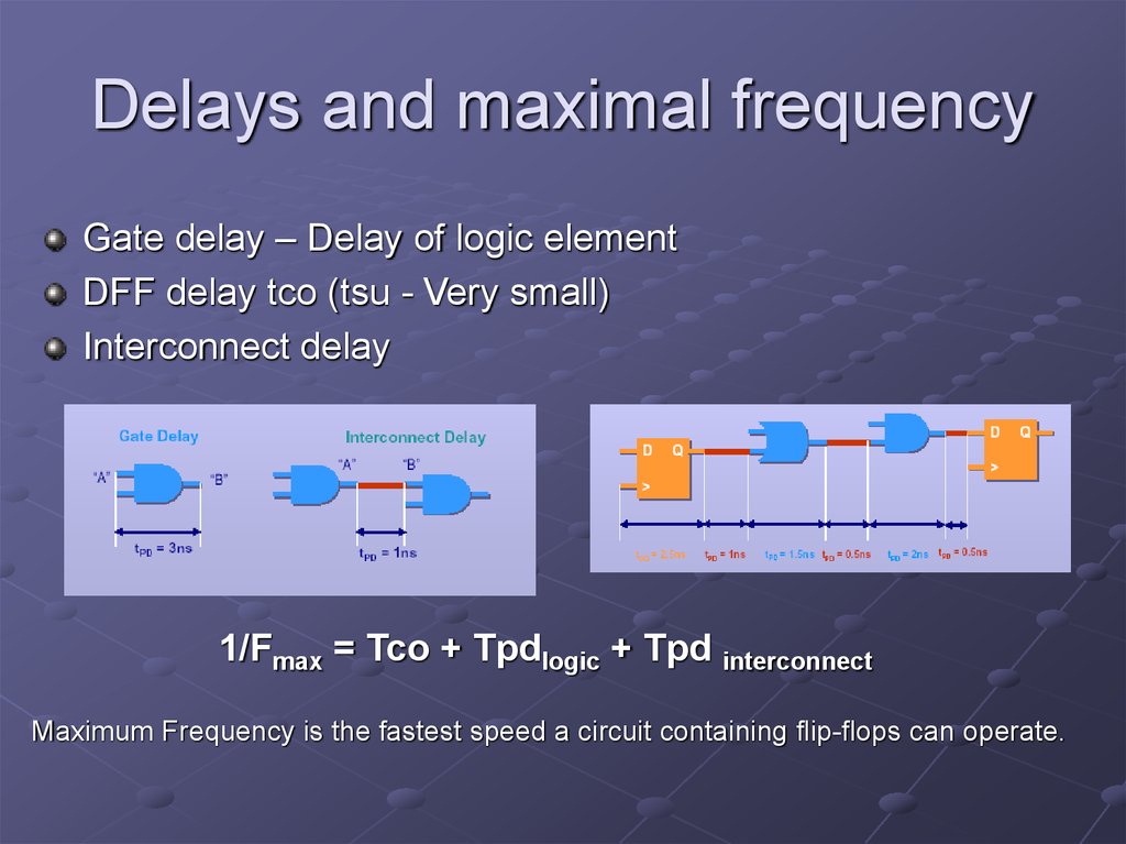
28. Delays and maximal frequency
Gate delay – Delay of logic elementDFF delay tco (tsu - Very small)
Interconnect delay
1/Fmax = Tco + Tpdlogic + Tpd interconnect
Maximum Frequency is the fastest speed a circuit containing flip-flops can operate.
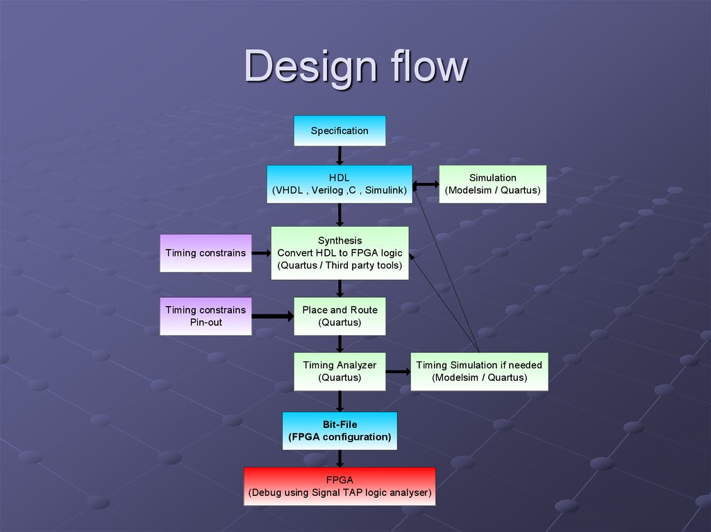
29. Design flow
SpecificationHDL
(VHDL , Verilog ,C , Simulink)
Timing constrains
Synthesis
Convert HDL to FPGA logic
(Quartus / Third party tools)
Timing constrains
Pin-out
Place and Route
(Quartus)
Timing Analyzer
(Quartus)
Simulation
(Modelsim / Quartus)
Timing Simulation if needed
(Modelsim / Quartus)
Bit-File
(FPGA configuration)
FPGA
(Debug using Signal TAP logic analyser)
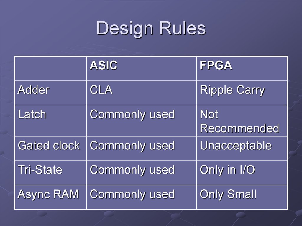
30. Design Rules
ASICFPGA
Adder
CLA
Ripple Carry
Latch
Commonly used
Gated clock Commonly used
Not
Recommended
Unacceptable
Tri-State
Commonly used
Only in I/O
Async RAM Commonly used
Only Small




 Электроника


