
 Электроника
Похожие презентации:


")
")


Shift Registers Lecture 11 Digital Electronics
1.
Shift RegistersLecture 11
Digital Electronics
2.
Course MaterialsAll needed Software and course materials will
be located on Canvas.
◻ Materials that are used in this slides are taken
from the textbook “Digital Electronics A
Practical Approach with VHDL” by William
Kleitz
◻
3.
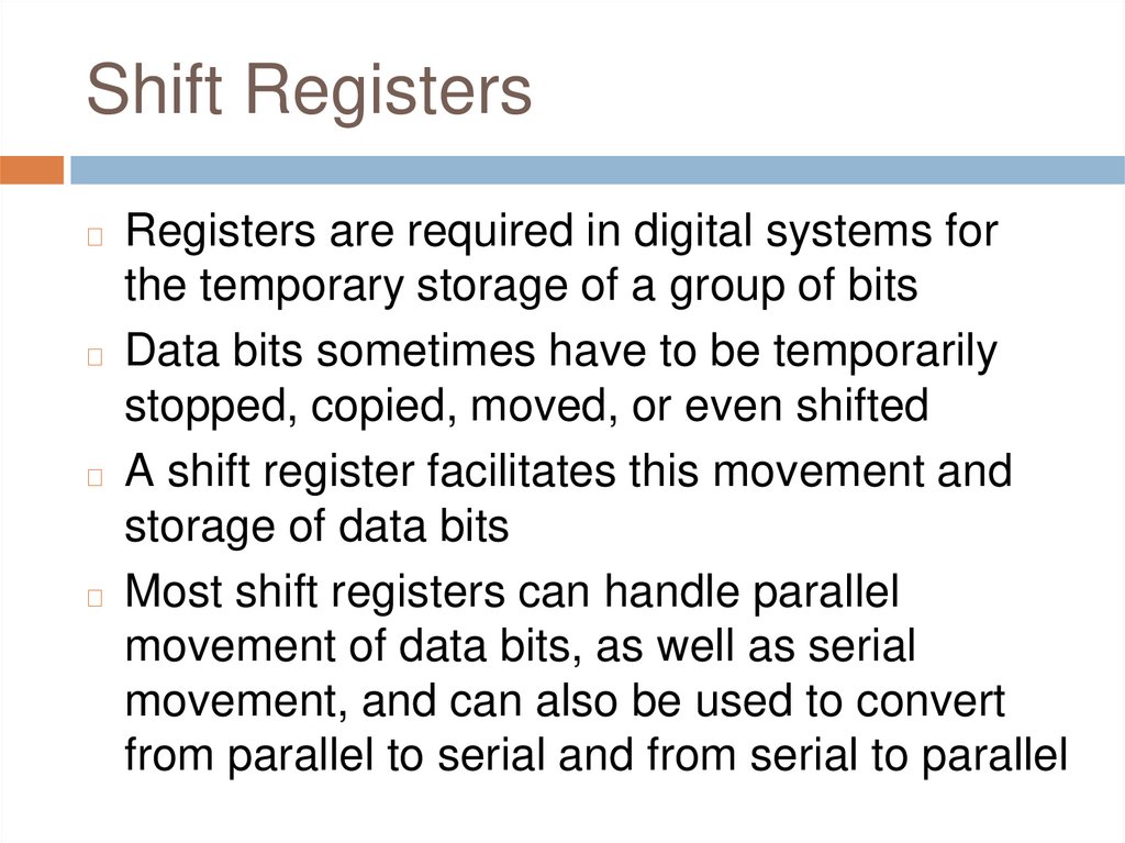
Shift RegistersRegisters are required in digital systems for
the temporary storage of a group of bits
◻ Data bits sometimes have to be temporarily
stopped, copied, moved, or even shifted
◻ A shift register facilitates this movement and
storage of data bits
◻ Most shift registers can handle parallel
movement of data bits, as well as serial
movement, and can also be used to convert
from parallel to serial and from serial to parallel
◻
4.
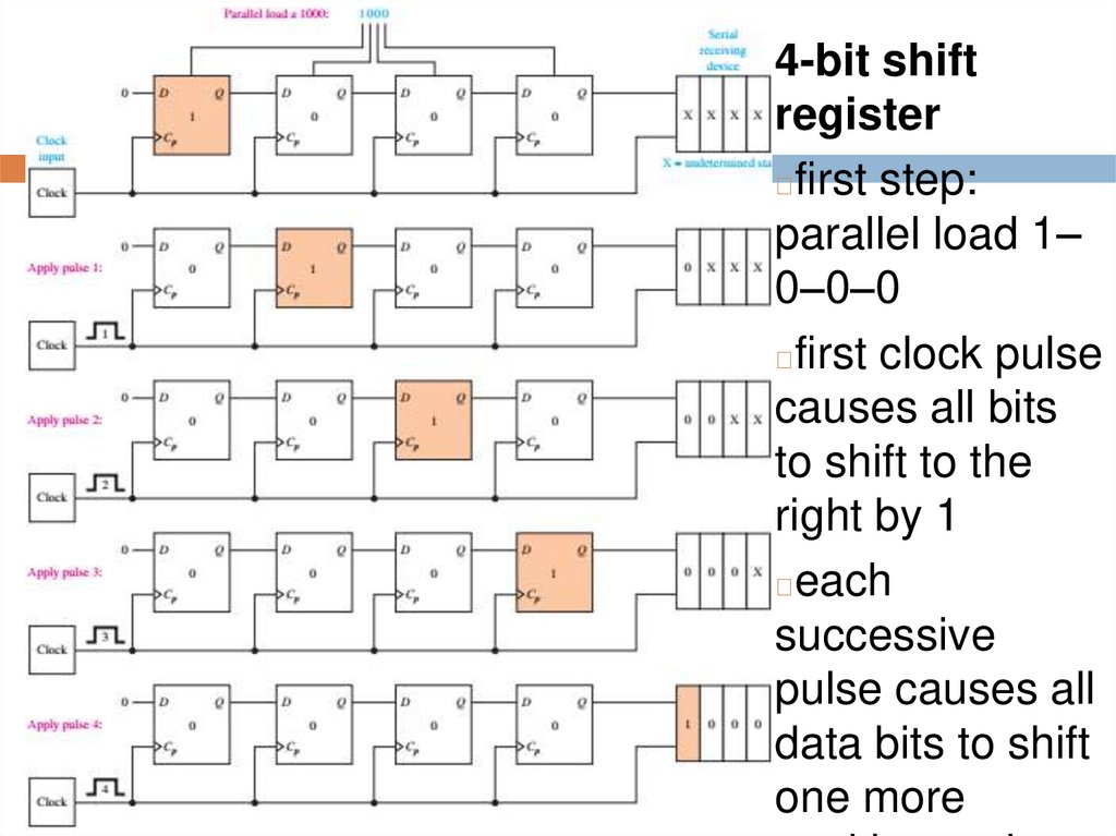
4-bit shiftregister
◻first step:
parallel load 1–
0–0–0
◻first clock pulse
causes all bits
to shift to the
right by 1
◻each
successive
pulse causes all
data bits to shift
one more
5.
4-bit Shift RegisterParallel load is done by momentarily enabling
the appropriate asynchronous Set and Reset
inputs
◻ At the end of the fourth clock pulse all four
original data bits appear, in the correct order,
in the serial receiving device
◻ Computers operate on data internally in a
parallel format
◻ To communicate over a serial cable like the
one used by the RS232 standard or a
telephone line, the data must first be converted
◻
6.
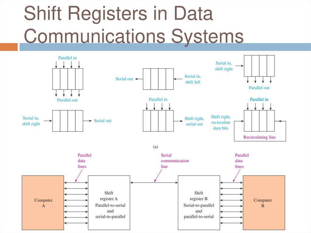
Shift Registers in DataCommunications Systems
7.
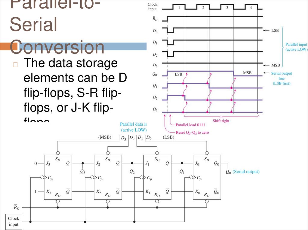
Parallel-toSerialConversion
◻
The data storage
elements can be D
flip-flops, S-R flipflops, or J-K flipflops
8.
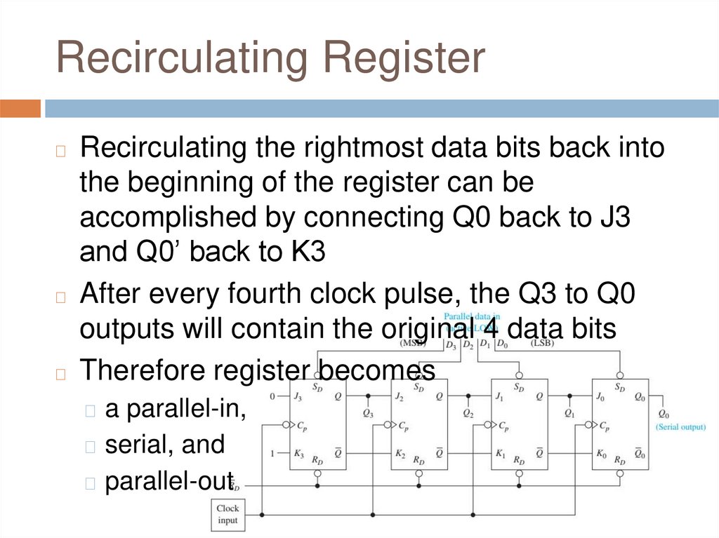
Recirculating RegisterRecirculating the rightmost data bits back into
the beginning of the register can be
accomplished by connecting Q0 back to J3
and Q0’ back to K3
◻ After every fourth clock pulse, the Q3 to Q0
outputs will contain the original 4 data bits
◻ Therefore register becomes
◻
◻ a parallel-in,
◻ serial, and
◻ parallel-out
9.
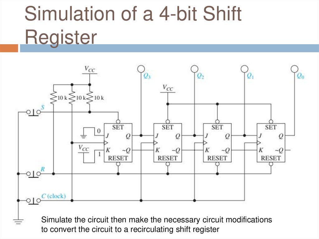
Simulation of a 4-bit ShiftRegister
Simulate the circuit then make the necessary circuit modifications
to convert the circuit to a recirculating shift register
10.
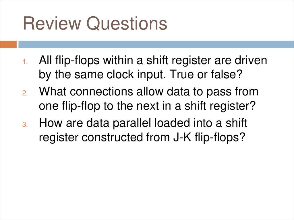
Review Questions1.
2.
3.
All flip-flops within a shift register are driven
by the same clock input. True or false?
What connections allow data to pass from
one flip-flop to the next in a shift register?
How are data parallel loaded into a shift
register constructed from J-K flip-flops?
11.
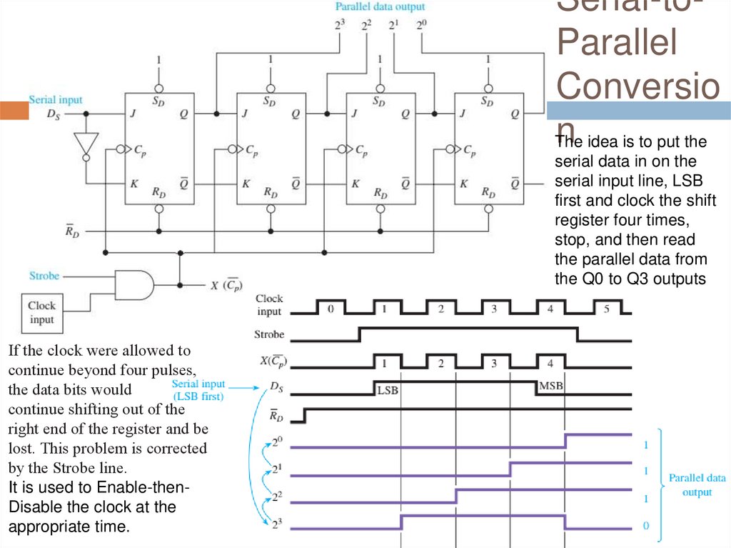
Serial-toParallelConversio
nhe idea is to put the
T
serial data in on the
serial input line, LSB
first and clock the shift
register four times,
stop, and then read
the parallel data from
the Q0 to Q3 outputs
If the clock were allowed to
continue beyond four pulses,
the data bits would
continue shifting out of the
right end of the register and be
lost. This problem is corrected
by the Strobe line.
It is used to Enable-thenDisable the clock at the
appropriate time.
12.
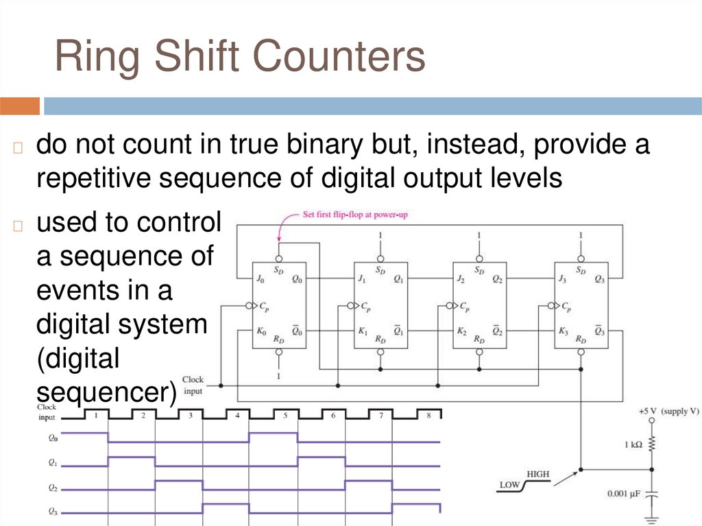
Ring Shift Counters◻
do not count in true binary but, instead, provide a
repetitive sequence of digital output levels
◻
used to control
a sequence of
events in a
digital system
(digital
sequencer)
13.
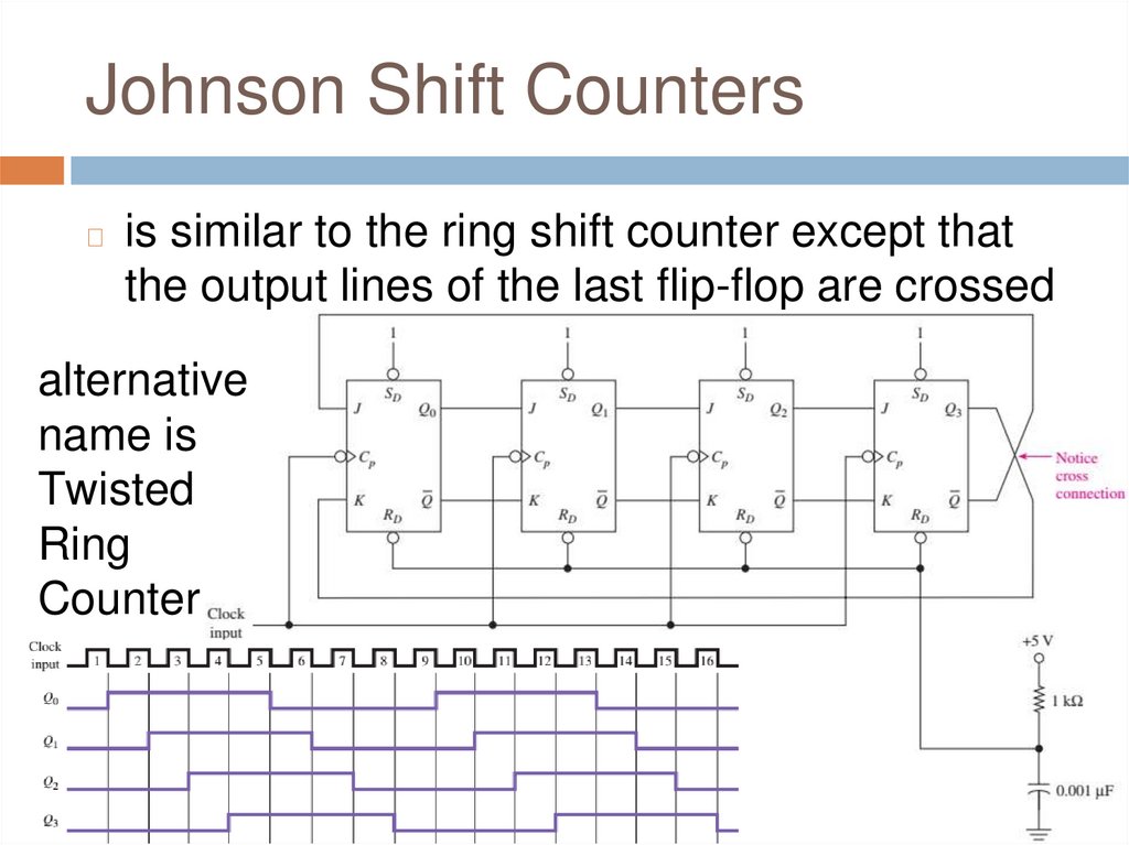
Johnson Shift Counters◻
is similar to the ring shift counter except that
the output lines of the last flip-flop are crossed
alternative
name is
Twisted
Ring
Counter
14.
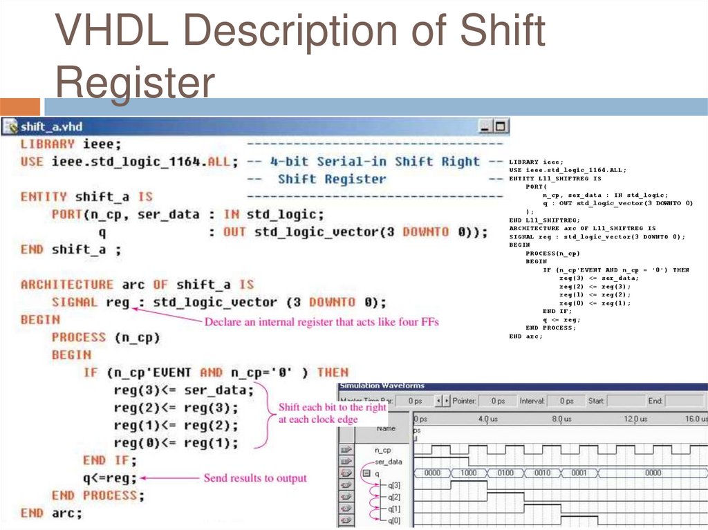
VHDL Description of ShiftRegister
LIBRARY ieee;
USE ieee.std_logic_1164.ALL;
ENTITY L11_SHIFTREG IS
PORT(
n_cp, ser_data : IN std_logic;
q : OUT std_logic_vector(3 DOWNTO 0)
);
END L11_SHIFTREG;
ARCHITECTURE arc OF L11_SHIFTREG IS
SIGNAL reg : std_logic_vector(3 DOWNTO 0);
BEGIN
PROCESS(n_cp)
BEGIN
IF (n_cp'EVENT AND n_cp = '0') THEN
reg(3) <= ser_data;
reg(2) <= reg(3);
reg(1) <= reg(2);
reg(0) <= reg(1);
END IF;
q <= reg;
END PROCESS;
END arc;
15.
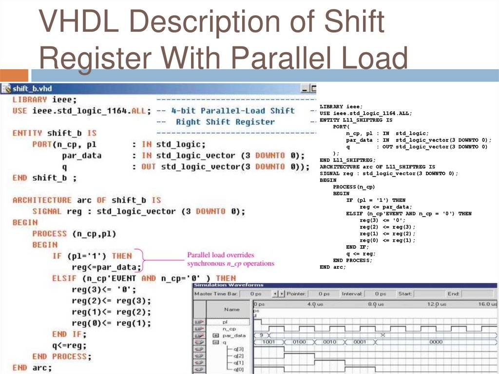
VHDL Description of ShiftRegister With Parallel Load
LIBRARY ieee;
USE ieee.std_logic_1164.ALL;
ENTITY L11_SHIFTREG IS
PORT(
n_cp, pl : IN std_logic;
par_data : IN std_logic_vector(3 DOWNTO 0);
q
: OUT std_logic_vector(3 DOWNTO 0)
);
END L11_SHIFTREG;
ARCHITECTURE arc OF L11_SHIFTREG IS
SIGNAL reg : std_logic_vector(3 DOWNTO 0);
BEGIN
PROCESS(n_cp)
BEGIN
IF (pl = '1') THEN
reg <= par_data;
ELSIF (n_cp'EVENT AND n_cp = '0') THEN
reg(3) <= '0';
reg(2) <= reg(3);
reg(1) <= reg(2);
reg(0) <= reg(1);
END IF;
q <= reg;
END PROCESS;
END arc;
16.
Shift Register ICs4-bit and 8-bit shift registers are commonly
available in IC packages
◻ practically every possible load, shift, and
conversion operation is available
◻ four popular shift register ICs:
◻
◻ 74164 8-Bit Serial-In, Parallel-Out Shift Register
◻ 74165 8-bit serial or parallel-in, serial-out shift
register
◻ 74194 4-bit bidirectional universal shift register
◻ 74395A 4-bit shift right register with three-state
outputs
17.
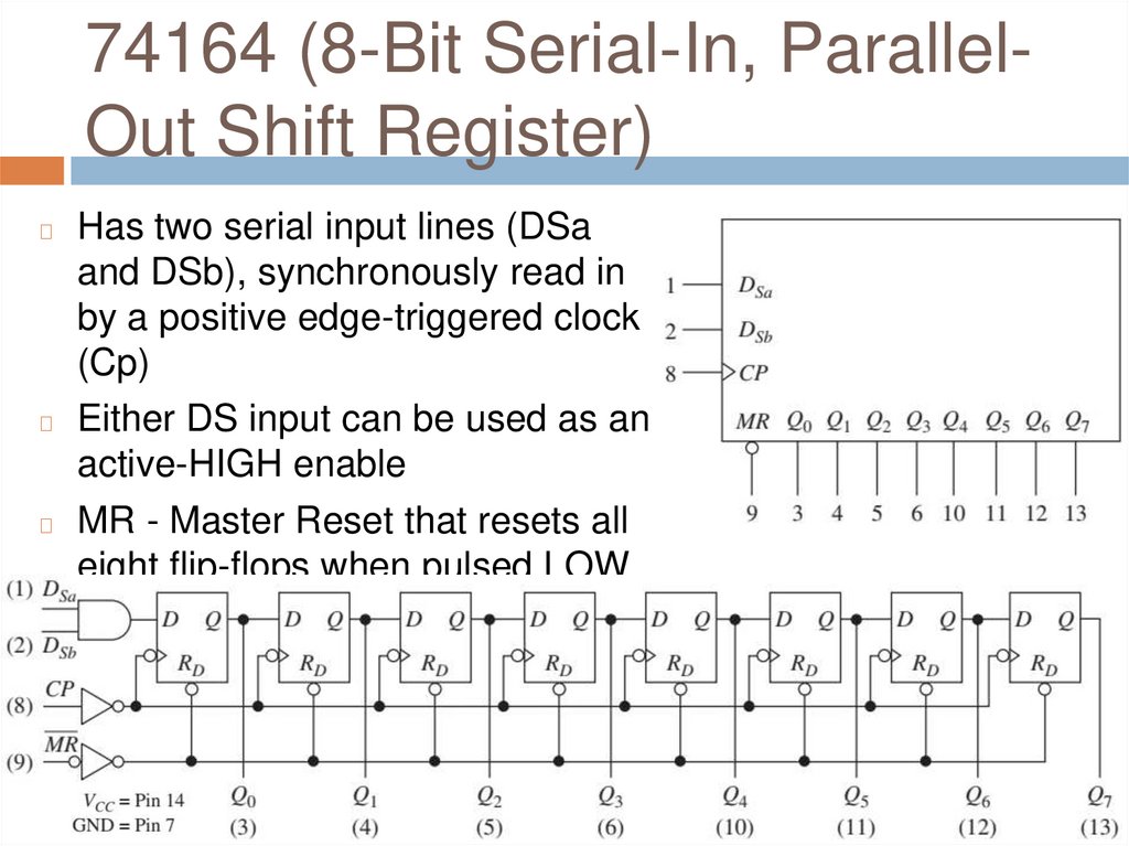
74164 (8-Bit Serial-In, ParallelOut Shift Register)Has two serial input lines (DSa
and DSb), synchronously read in
by a positive edge-triggered clock
(Cp)
◻ Either DS input can be used as an
active-HIGH enable
◻ MR - Master Reset that resets all
eight flip-flops when pulsed LOW
◻
18.
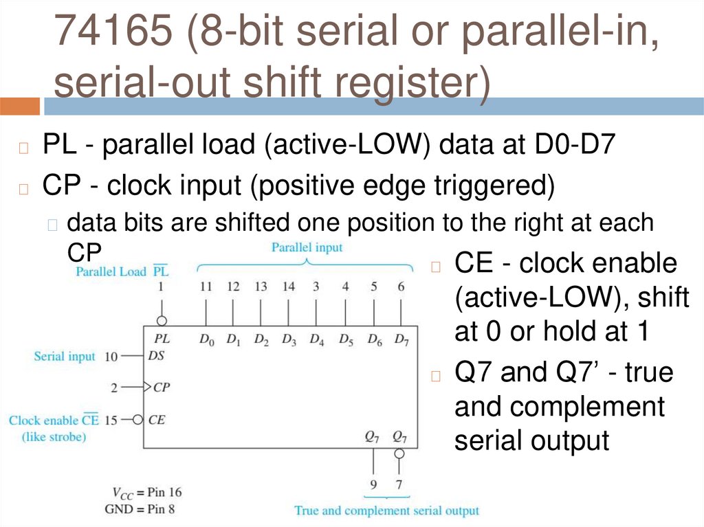
74165 (8-bit serial or parallel-in,serial-out shift register)
PL - parallel load (active-LOW) data at D0-D7
◻ CP - clock input (positive edge triggered)
◻
◻ data bits are shifted one position to the right at each
CP
CE - clock enable
(active-LOW), shift
at 0 or hold at 1
◻ Q7 and Q7’ - true
and complement
serial output
◻
19.
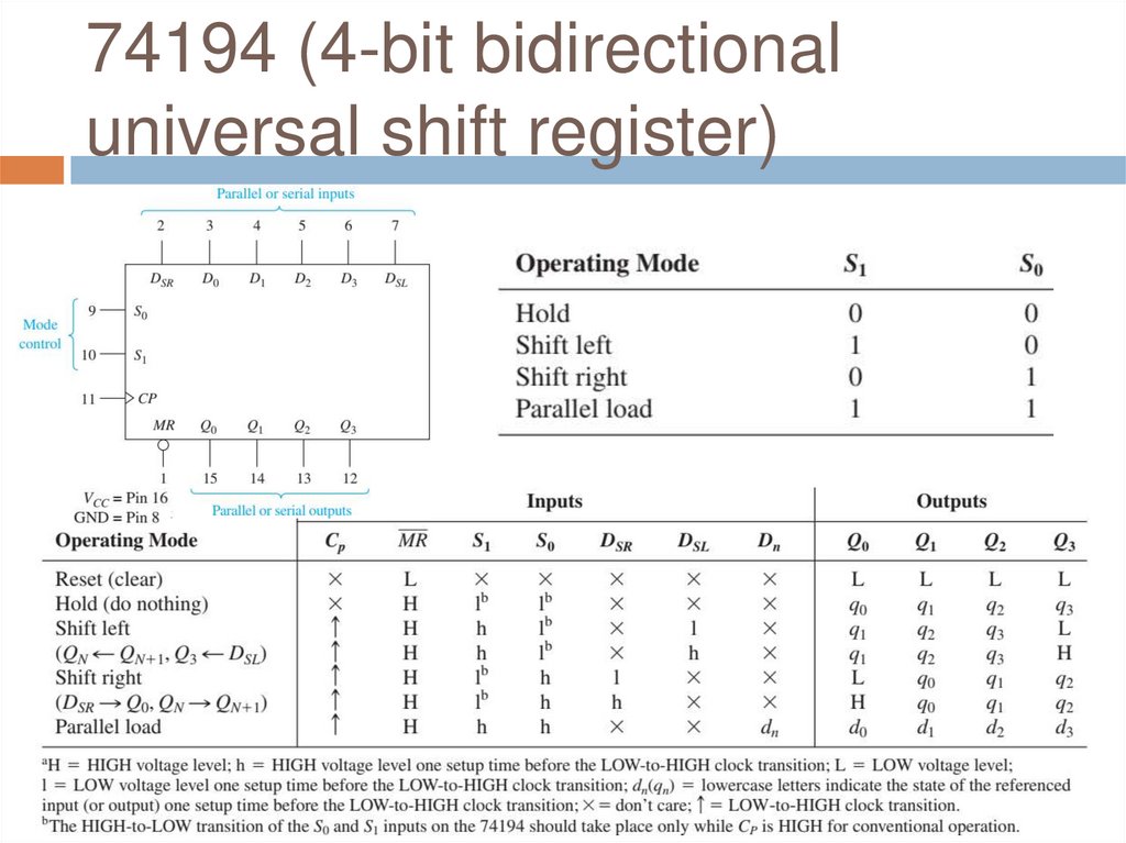
74194 (4-bit bidirectionaluniversal shift register)
20.
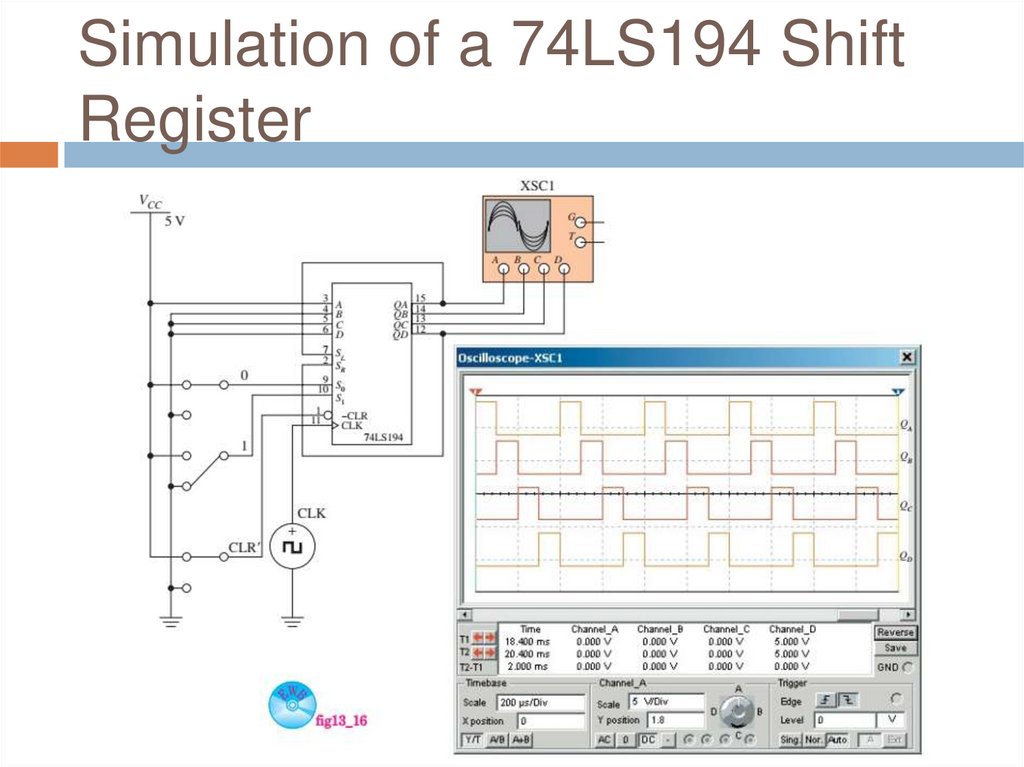
Simulation of a 74LS194 ShiftRegister
21.
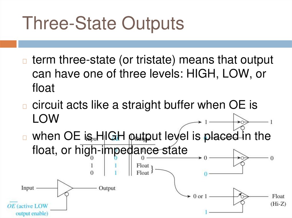
Three-State Outputsterm three-state (or tristate) means that output
can have one of three levels: HIGH, LOW, or
float
◻ circuit acts like a straight buffer when OE is
LOW
◻ when OE is HIGH output level is placed in the
float, or high-impedance state
◻
22.
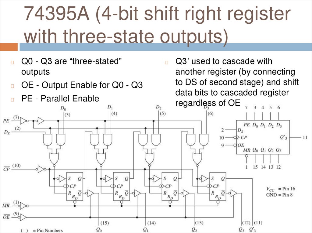
74395A (4-bit shift right registerwith three-state outputs)
◻
Q0 - Q3 are “three-stated”
outputs
◻
OE - Output Enable for Q0 - Q3
◻
PE - Parallel Enable
◻
MR - Master Reset
◻
Q3’ used to cascade with
another register (by connecting
to DS of second stage) and shift
data bits to cascaded register
regardless of OE
23.
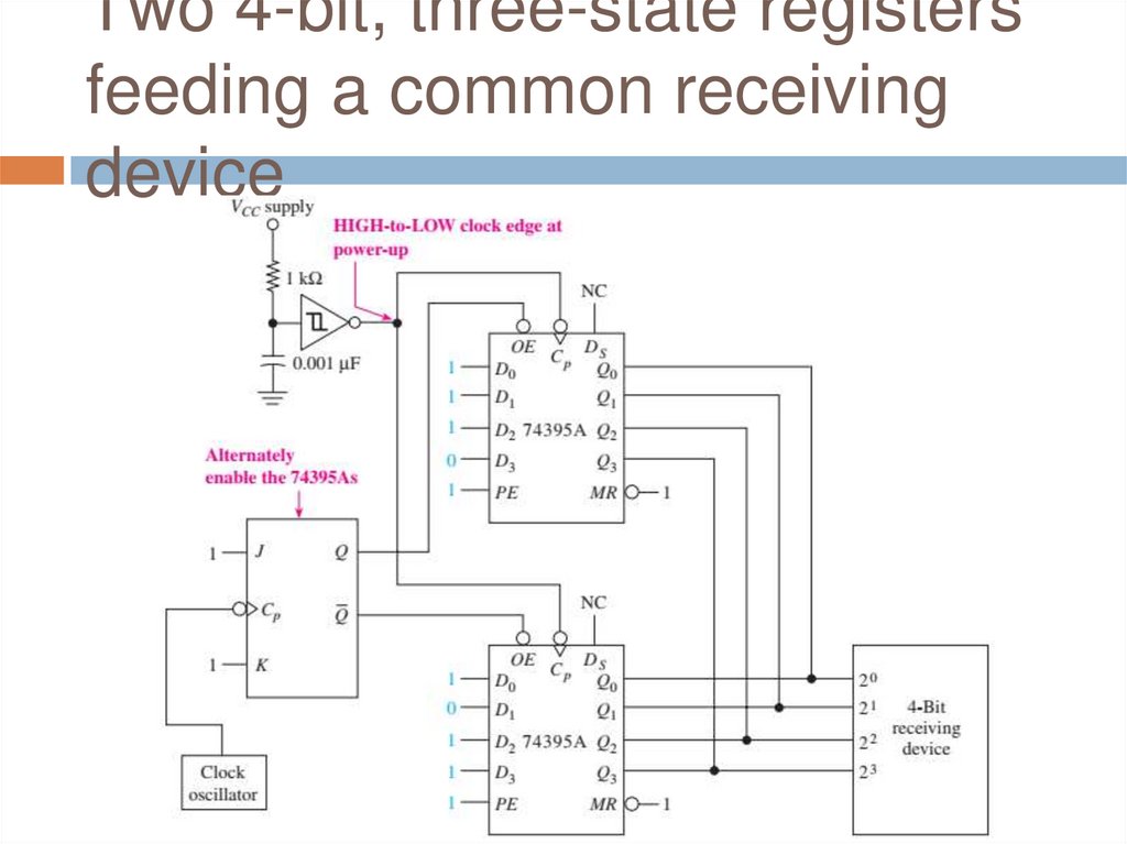
Two 4-bit, three-state registersfeeding a common receiving
device
24.
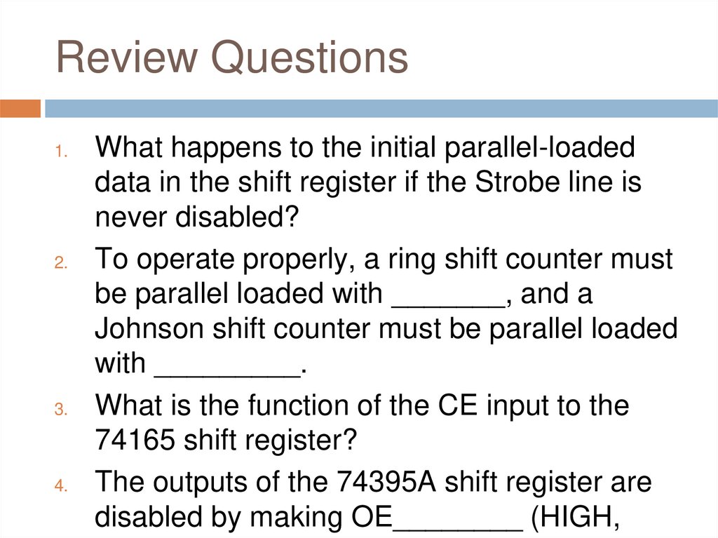
Review Questions1.
2.
3.
4.
What happens to the initial parallel-loaded
data in the shift register if the Strobe line is
never disabled?
To operate properly, a ring shift counter must
be parallel loaded with _______, and a
Johnson shift counter must be parallel loaded
with _________.
What is the function of the CE input to the
74165 shift register?
The outputs of the 74395A shift register are
disabled by making OE________ (HIGH,
25.
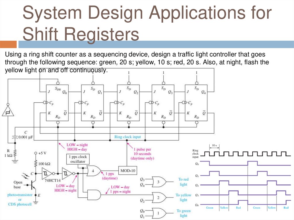
System Design Applications forShift Registers
Using a ring shift counter as a sequencing device, design a traffic light controller that goes
through the following sequence: green, 20 s; yellow, 10 s; red, 20 s. Also, at night, flash the
yellow light on and off continuously.
26.
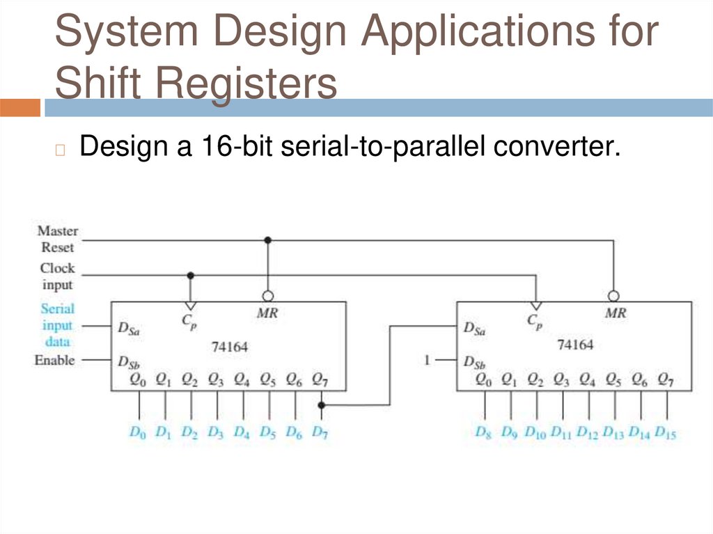
System Design Applications forShift Registers
◻
Design a 16-bit serial-to-parallel converter.
27.
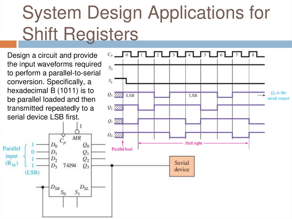
System Design Applications forShift Registers
Design a circuit and provide
the input waveforms required
to perform a parallel-to-serial
conversion. Specifically, a
hexadecimal B (1011) is to
be parallel loaded and then
transmitted repeatedly to a
serial device LSB first.
28.
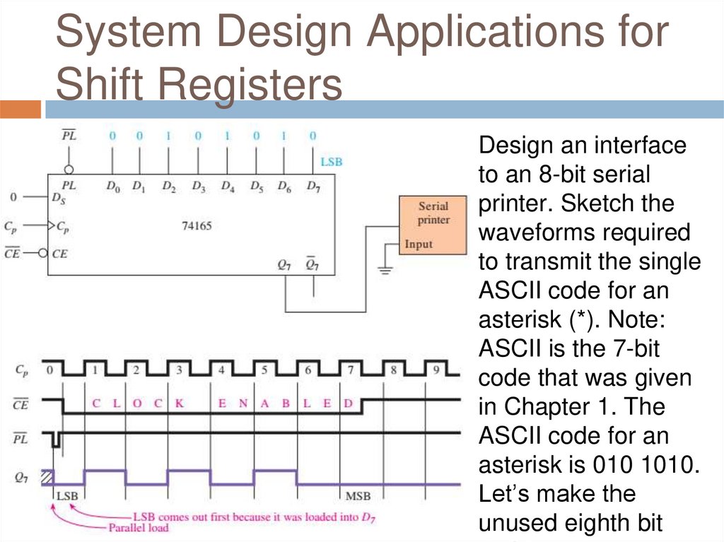
System Design Applications forShift Registers
Design an interface
to an 8-bit serial
printer. Sketch the
waveforms required
to transmit the single
ASCII code for an
asterisk (*). Note:
ASCII is the 7-bit
code that was given
in Chapter 1. The
ASCII code for an
asterisk is 010 1010.
Let’s make the
unused eighth bit
29.
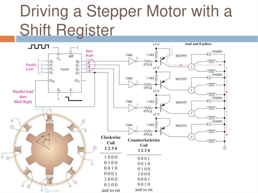
Driving a Stepper Motor with aShift Register
30.
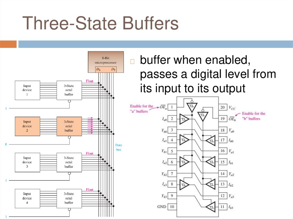
Three-State Buffers◻
buffer when enabled,
passes a digital level from
its input to its output
unchanged
31.
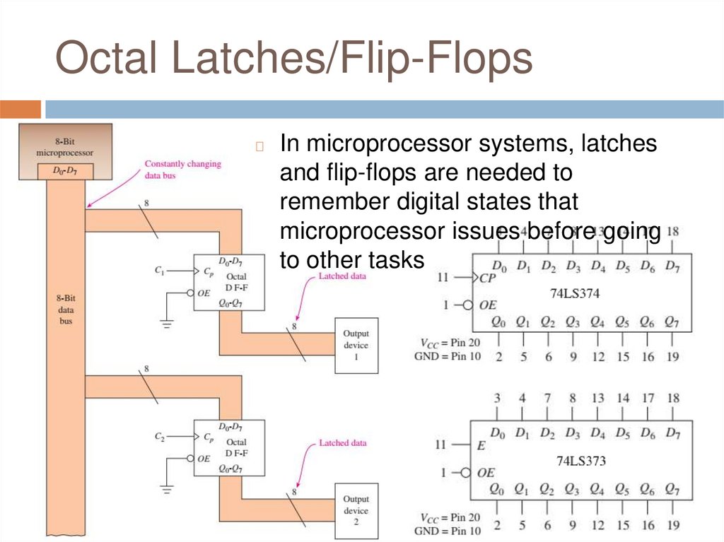
Octal Latches/Flip-Flops◻
In microprocessor systems, latches
and flip-flops are needed to
remember digital states that
microprocessor issues before going
to other tasks
32.
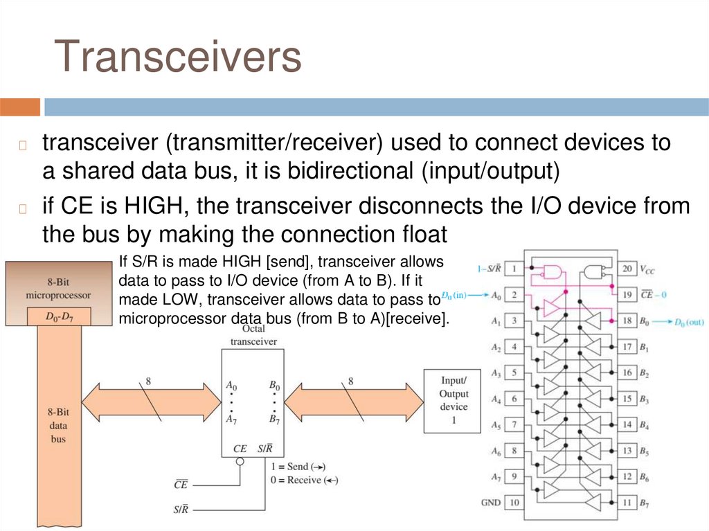
Transceiverstransceiver (transmitter/receiver) used to connect devices to
a shared data bus, it is bidirectional (input/output)
◻ if CE is HIGH, the transceiver disconnects the I/O device from
the bus by making the connection float
◻
If S/R is made HIGH [send], transceiver allows
data to pass to I/O device (from A to B). If it
made LOW, transceiver allows data to pass to
microprocessor data bus (from B to A)[receive].
33.
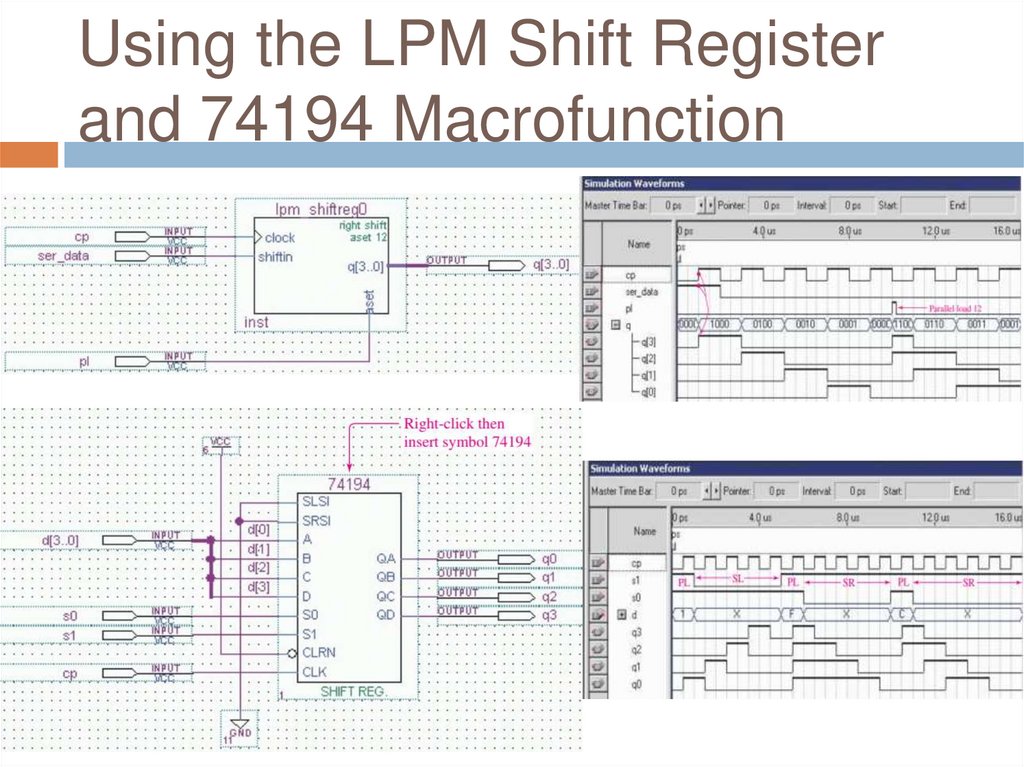
Using the LPM Shift Registerand 74194 Macrofunction
34.
Using VHDL Components andInstantiations
structural VHDL programs use multiple
components
◻ components are predefined VHDL program
modules
◻
◻ can be used repeatedly like subroutines in a PL
◻ Ex: the key component in a shift register is a D
flip-flop
◻
D flip-flop entity and its architecture must first
be defined at the beginning of the VHDL
program
◻ or it may be previously defined and stored in a
35.
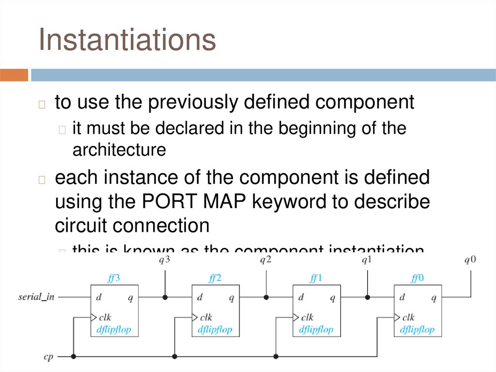
Instantiations◻
to use the previously defined component
◻ it must be declared in the beginning of the
architecture
◻
each instance of the component is defined
using the PORT MAP keyword to describe
circuit connection
◻ this is known as the component instantiation
36.
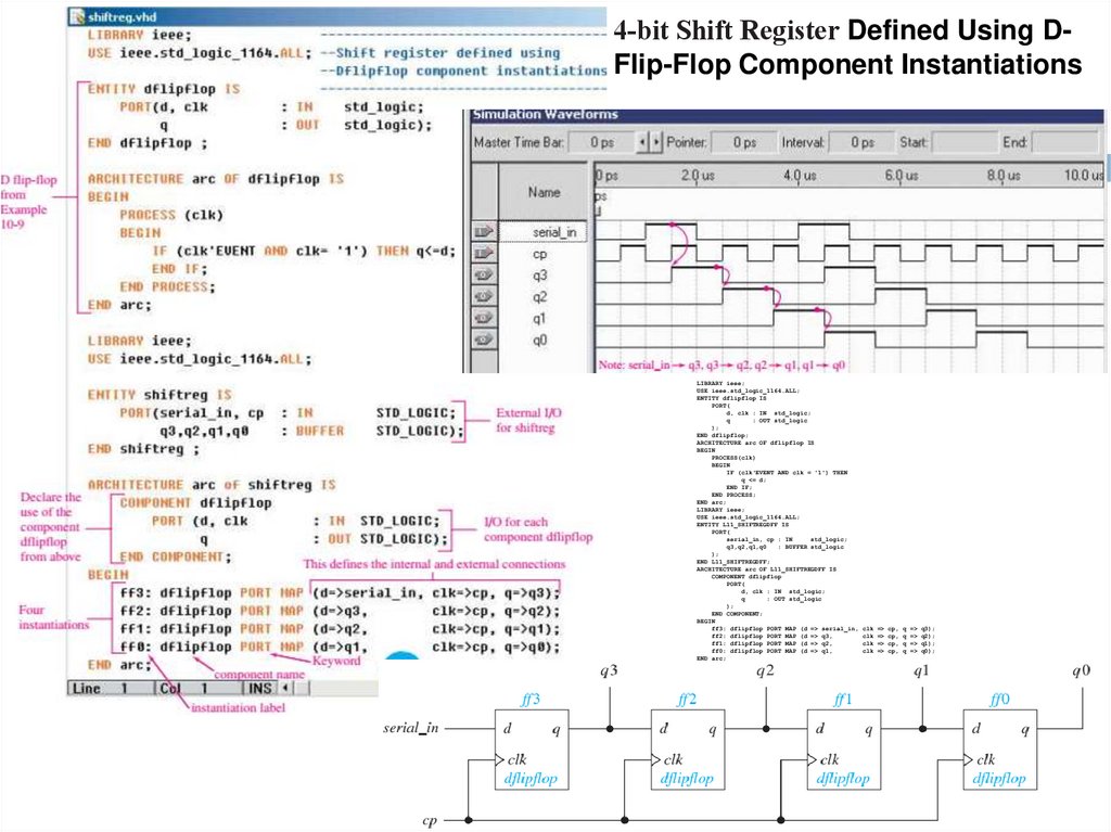
4-bit Shift Register Defined Using DFlip-Flop Component InstantiationsLIBRARY ieee;
USE ieee.std_logic_1164.ALL;
ENTITY dflipflop IS
PORT(
d, clk : IN std_logic;
q
: OUT std_logic
);
END dflipflop;
ARCHITECTURE arc OF dflipflop IS
BEGIN
PROCESS(clk)
BEGIN
IF (clk'EVENT AND clk = '1') THEN
q <= d;
END IF;
END PROCESS;
END arc;
LIBRARY ieee;
USE ieee.std_logic_1164.ALL;
ENTITY L11_SHIFTREGDFF IS
PORT(
serial_in, cp : IN
std_logic;
q3,q2,q1,q0
: BUFFER std_logic
);
END L11_SHIFTREGDFF;
ARCHITECTURE arc OF L11_SHIFTREGDFF IS
COMPONENT dflipflop
PORT(
d, clk : IN std_logic;
q
: OUT std_logic
);
END COMPONENT;
BEGIN
ff3: dflipflop PORT MAP (d => serial_in, clk => cp, q => q3);
ff2: dflipflop PORT MAP (d => q3,
clk => cp, q => q2);
ff1: dflipflop PORT MAP (d => q2,
clk => cp, q => q1);
ff0: dflipflop PORT MAP (d => q1,
clk => cp, q => q0);
END arc;
37.
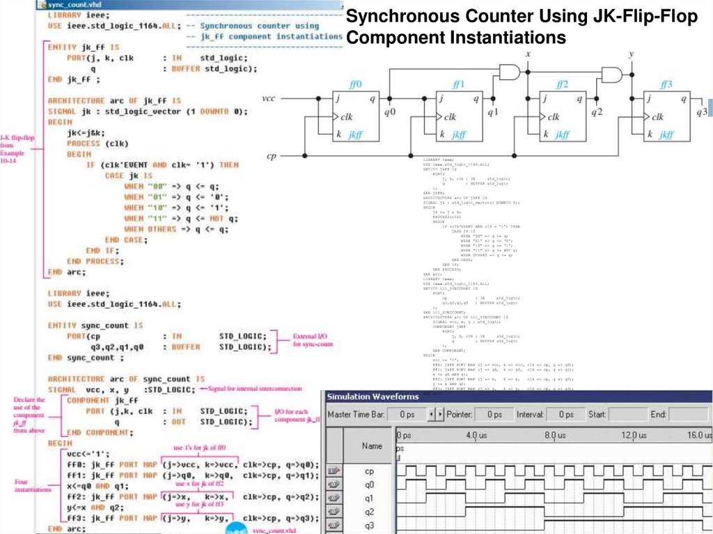
Synchronous Counter Using JK-Flip-FlopComponent Instantiations
LIBRARY ieee;
USE ieee.std_logic_1164.ALL;
ENTITY jkff IS
PORT(
j, k, clk : IN
std_logic;
q
: BUFFER std_logic
);
END jkff;
ARCHITECTURE arc OF jkff IS
SIGNAL jk : std_logic_vector(1 DOWNTO 0);
BEGIN
jk <= j & k;
PROCESS(clk)
BEGIN
IF (clk'EVENT AND clk = '1') THEN
CASE jk IS
WHEN "00" => q <= q;
WHEN "01" => q <= '0';
WHEN "10" => q <= '1';
WHEN "11" => q <= NOT q;
WHEN OTHERS => q <= q;
END CASE;
END IF;
END PROCESS;
END arc;
LIBRARY ieee;
USE ieee.std_logic_1164.ALL;
ENTITY L11_SYNCCOUNT IS
PORT(
cp
: IN
std_logic;
q3,q2,q1,q0
: BUFFER std_logic
);
END L11_SYNCCOUNT;
ARCHITECTURE arc OF L11_SYNCCOUNT IS
SIGNAL vcc, x, y : std_logic;
COMPONENT jkff
PORT(
j, k, clk : IN
std_logic;
q
: BUFFER std_logic
);
END COMPONENT;
BEGIN
vcc <= '1';
ff0: jkff PORT MAP (j => vcc, k => vcc, clk => cp, q => q0);
ff1: jkff PORT MAP (j => q0, k => q0, clk => cp, q => q1);
x <= q0 AND q1;
ff2: jkff PORT MAP (j => x,
k => x,
clk => cp, q => q2);
y <= x AND q2;
ff3: jkff PORT MAP (j => y,
k => y,
clk => cp, q => q3);
END arc;
38.
Q&AAny Questions?