Похожие презентации:
Digital Systems. Chapter 5. Flip-Flops and Related Devices
1. DIGITAL CIRCUIT, 2023-1 RAJIB PAUL
Digital SystemsChapter 5 – Flip-Flops and Related Devices
DIGITAL CIRCUIT, 2023-1
RAJIB PAUL
Copyright © 2011, 2007, 2004, 2001, 1998 by Pearson Education, Inc.
Upper Saddle River, New Jersey 07458 • All rights reserved
2. Chapter 5 Objectives
• Selected areas covered in this chapter:– Constructing/analyzing operation of latch flip-flops
made from NAND or NOR gates.
– Differences of synchronous/asynchronous systems.
– Major differences between parallel & serial transfers.
– Operation of edge-triggered flip-flops.
– Typical characteristics of Schmitt triggers.
– Effects of clock skew on synchronous circuits.
– Troubleshoot various types of flip-flop circuits.
– Sequential circuits with PLDs using schematic entry.
– Logic primitives, components & libraries in HDL code.
– Structural level circuits from components.
2
3. Chapter 5 Introduction
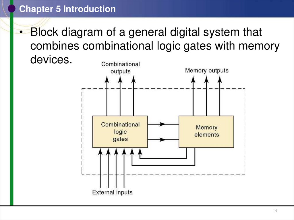
• Block diagram of a general digital system thatcombines combinational logic gates with memory
devices.
3
4. Chapter 5 Introduction
• The most important memory element is the flipflop (FF)—made up of an assembly of logic gates.The flip-flop is known by other names,
including latch and bistable multivibrator.
4
5. 5-1 NAND Gate Latch
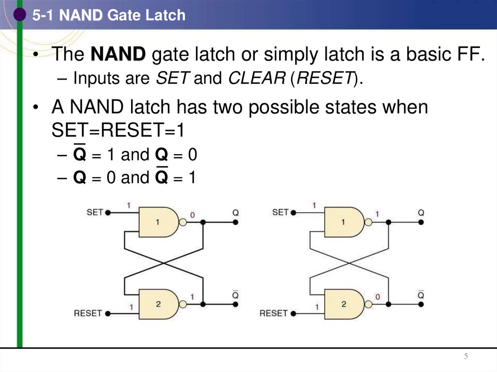
• The NAND gate latch or simply latch is a basic FF.– Inputs are SET and CLEAR (RESET).
• A NAND latch has two possible states when
SET=RESET=1
– Q = 1 and Q = 0
– Q = 0 and Q = 1
5
6. 5-1 NAND Gate Latch – Setting the Latch (FF)
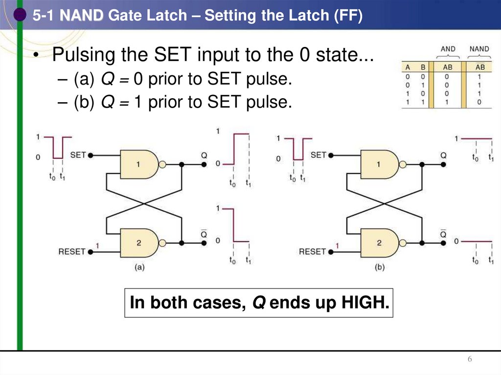
• Pulsing the SET input to the 0 state...– (a) Q = 0 prior to SET pulse.
– (b) Q = 1 prior to SET pulse.
In both cases, Q ends up HIGH.
6
7. 5-1 NAND Gate Latch – Resetting the Latch (FF)
• Pulsing RESET LOW when...– (a) Q = 0 prior to the RESET pulse.
– (b) Q = 1 prior to the RESET pulse.
In each case, Q ends up LOW.
7
8.
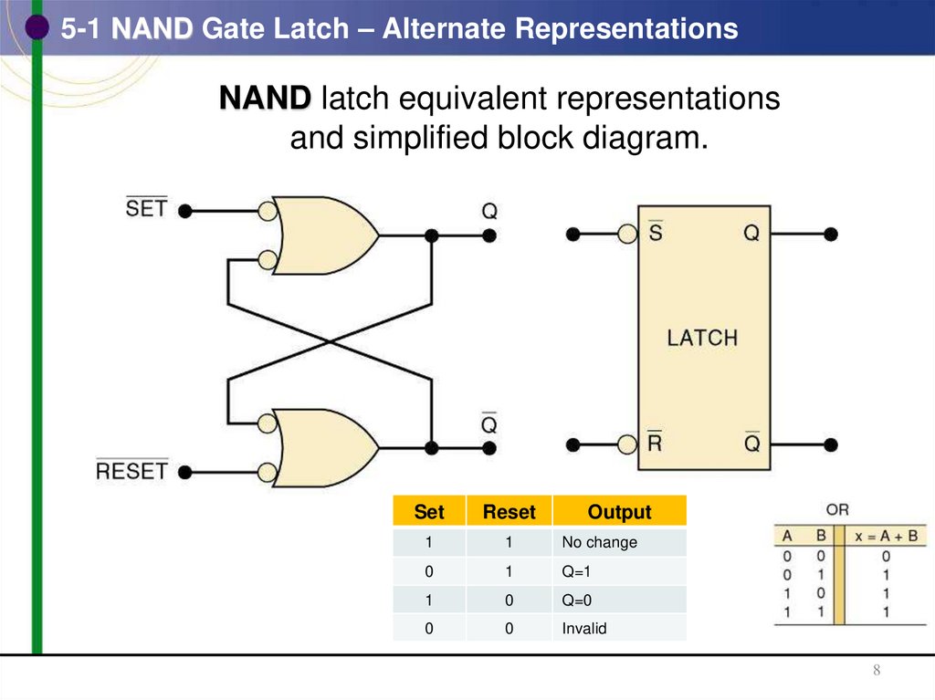
5-1 NAND Gate Latch – Alternate RepresentationsNAND latch equivalent representations
and simplified block diagram.
Set
Reset
Output
1
1
No change
0
1
Q=1
1
0
Q=0
0
0
Invalid
8
9. 5-1 NAND Gate Latch - Summary
• Summary of the NAND latch:– SET = 1, RESET = 1—Normal resting state, outputs
remain in state they were in prior to input.
– SET = 0, RESET = 1—Output will go to Q = 1 and
remains there, even after SET returns HIGH.
• Called setting the latch.
– SET = 1, RESET = 0—Will produce Q = 0 and
remains there, even after RESET returns HIGH.
• Called clearing or resetting the latch.
– SET = 0, RESET = 0—Tries to set and clear the latch
at the same time, and produces Q = Q = 1.
• Output is unpredictable, and this input condition
should not be used.
9
10. 5-2 NOR Gate Latch
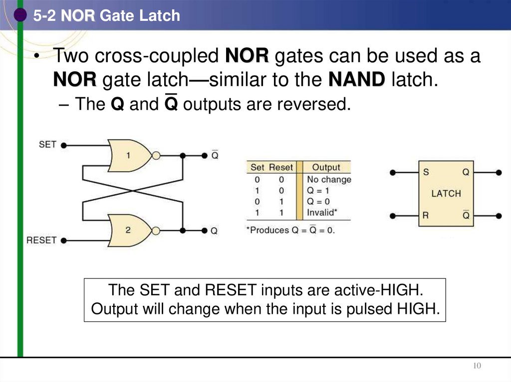
• Two cross-coupled NOR gates can be used as aNOR gate latch—similar to the NAND latch.
– The Q and Q outputs are reversed.
The SET and RESET inputs are active-HIGH.
Output will change when the input is pulsed HIGH.
10
11. 5-2 NOR Gate Latch - Summary
• Summary of the NOR latch:– SET = 0, RESET = 0—Normal resting state, No effect
on output state.
– SET = 1, RESET = 0—will always set Q = 1, where it
remains even after SET returns to 0.
– SET = 0, RESET = 1—will always clear Q = 0, where
it remains even after RESET returns to 0.
– SET = 1, RESET = 1—Tries to set and reset the latch
at the same time, and produces Q = Q = 0.
• Output is unpredictable, and this input condition
should not be used.
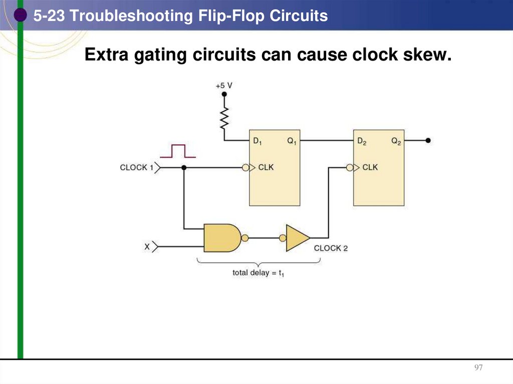
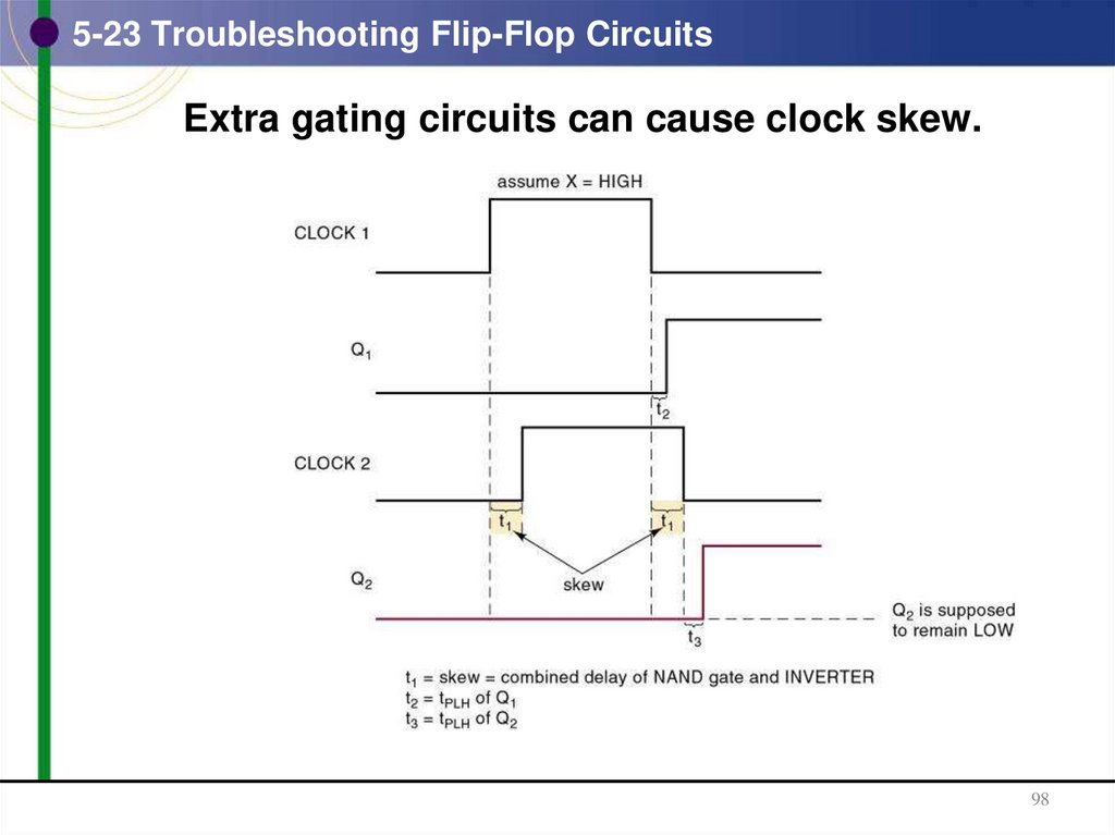
11
12. Example
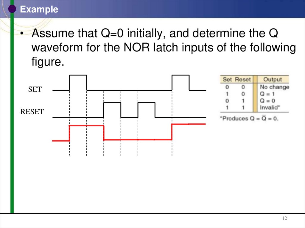
• Assume that Q=0 initially, and determine the Qwaveform for the NOR latch inputs of the following
figure.
SET
RESET
12
13. 5-2 Power-Up
• When power is applied, it is not possible to predictthe starting state of a flip-flop’s output.
– If SET and RESET inputs are in their inactive state.
• To start a latch or FF in a particular state, it must
be placed in that state by momentarily activating
the SET or RESET input, at the start of operation.
– Often achieved by application of a pulse to the
appropriate input.
13
14. 5-3 Troubleshooting Case Study
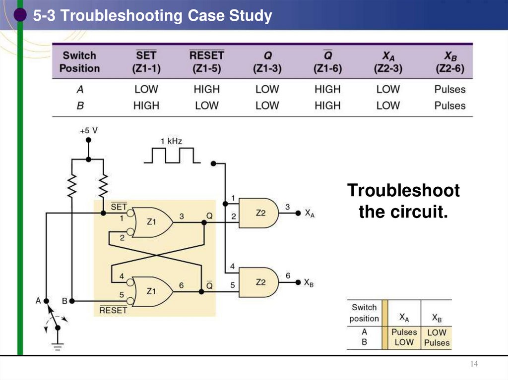
Troubleshootthe circuit.
14
15. 5-3 Troubleshooting Case Study
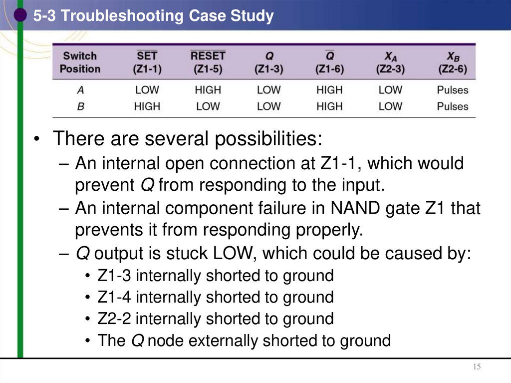
• There are several possibilities:– An internal open connection at Z1-1, which would
prevent Q from responding to the input.
– An internal component failure in NAND gate Z1 that
prevents it from responding properly.
– Q output is stuck LOW, which could be caused by:
• Z1-3 internally shorted to ground
• Z1-4 internally shorted to ground
• Z2-2 internally shorted to ground
• The Q node externally shorted to ground
15
16. 5-4 Digital Pulses
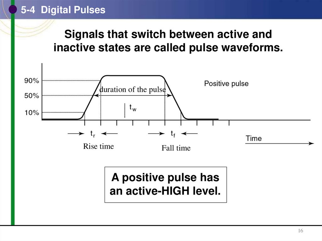
Signals that switch between active andinactive states are called pulse waveforms.
duration of the pulse
Rise time
Fall time
A positive pulse has
an active-HIGH level.
16
17. 5-4 Digital Pulses
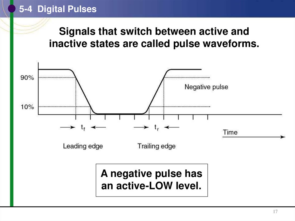
Signals that switch between active andinactive states are called pulse waveforms.
A negative pulse has
an active-LOW level.
17
18. 5-4 Digital Pulses
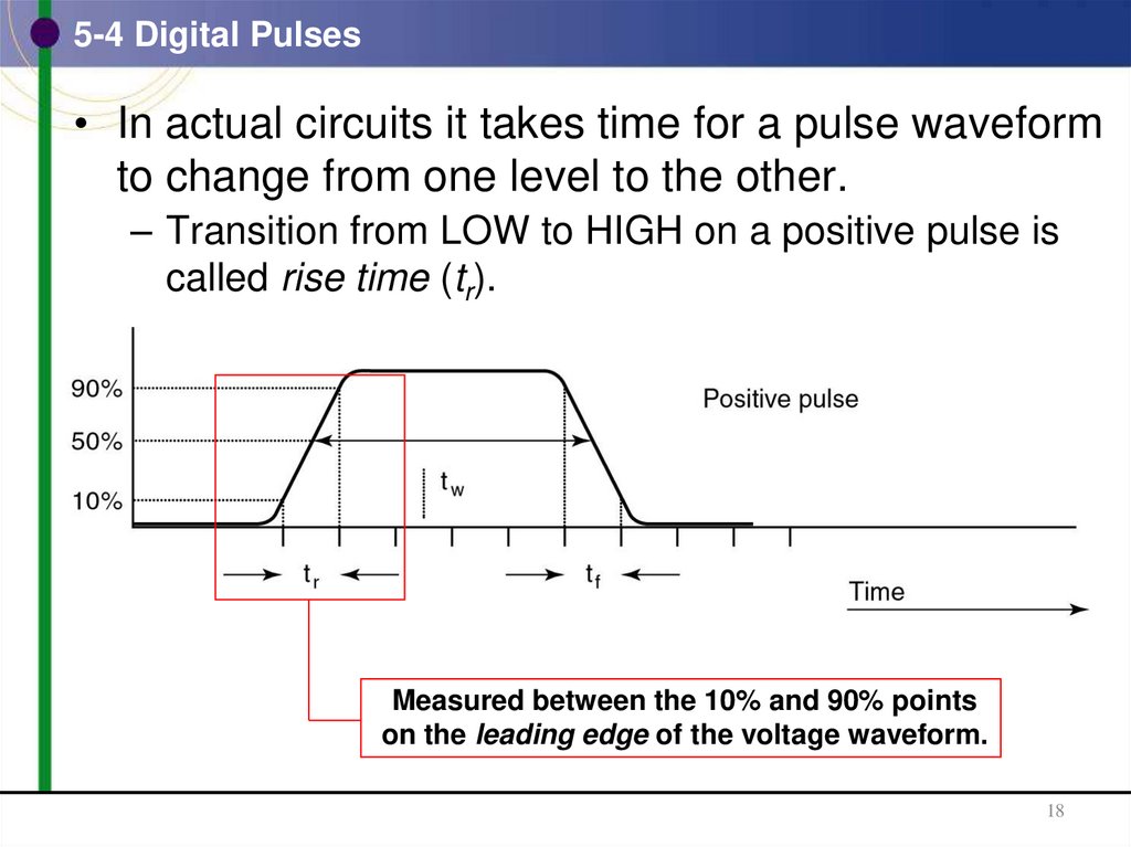
• In actual circuits it takes time for a pulse waveformto change from one level to the other.
– Transition from LOW to HIGH on a positive pulse is
called rise time (tr).
Measured between the 10% and 90% points
on the leading edge of the voltage waveform.
18
19. 5-4 Digital Pulses
• In actual circuits it takes time for a pulse waveformto change from one level to the other.
– Transition from HIGH to LOW on a positive pulse is
called fall time (tf).
Measured between the 90%
and 10% points on the trailing
edge of the voltage waveform.
19
20. 5-4 Digital Pulses
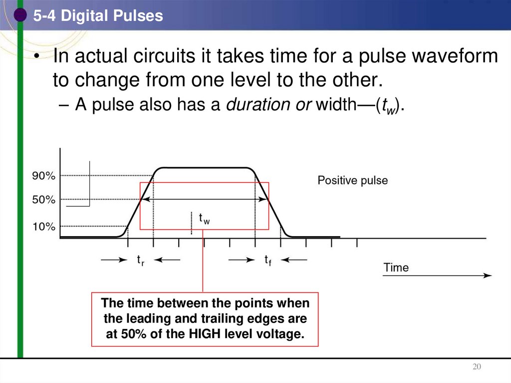
• In actual circuits it takes time for a pulse waveformto change from one level to the other.
– A pulse also has a duration or width—(tw).
The time between the points when
the leading and trailing edges are
at 50% of the HIGH level voltage.
20
21. 5-5 Clock Signals and Clocked Flip-Flops
• Digital systems can operate either asynchronouslyor synchronously.
– Asynchronous system—outputs can change state
at any time the input(s) change.
– Synchronous system—output can change state
only at a specific time in the clock cycle.
21
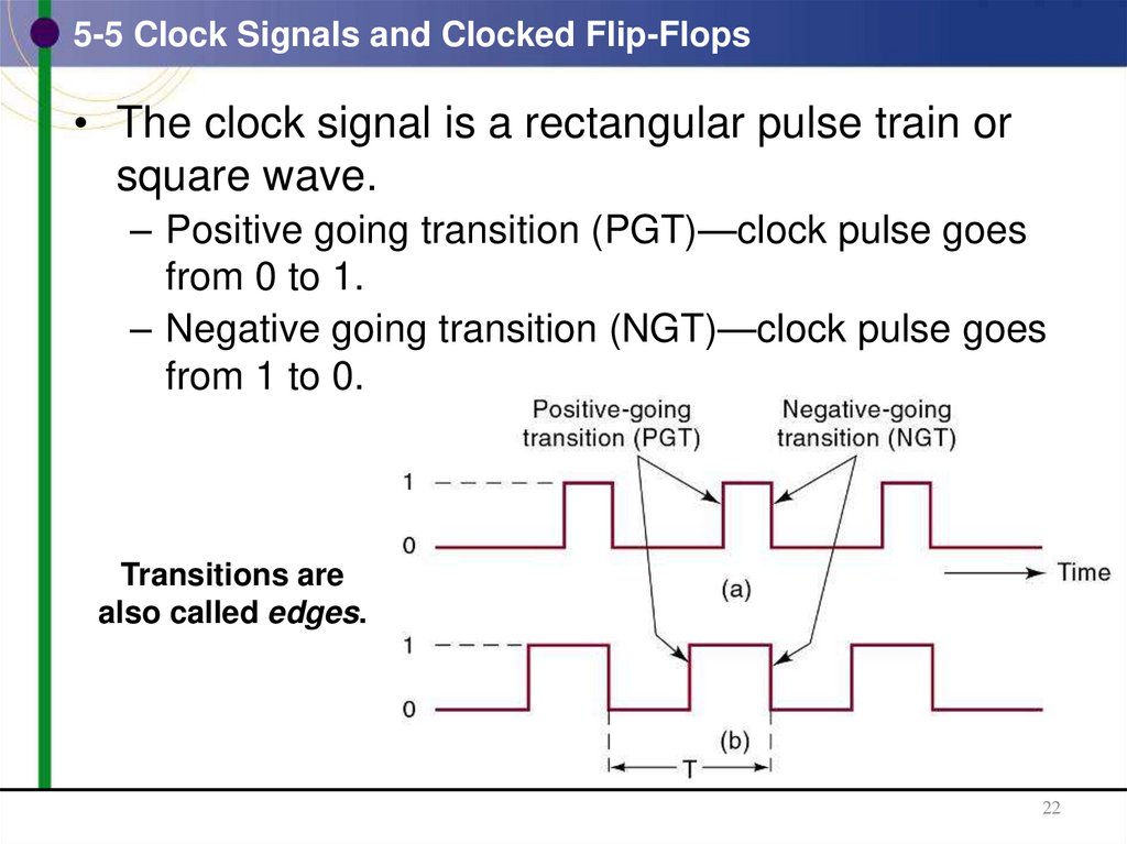
22. 5-5 Clock Signals and Clocked Flip-Flops
• The clock signal is a rectangular pulse train orsquare wave.
– Positive going transition (PGT)—clock pulse goes
from 0 to 1.
– Negative going transition (NGT)—clock pulse goes
from 1 to 0.
Transitions are
also called edges.
22
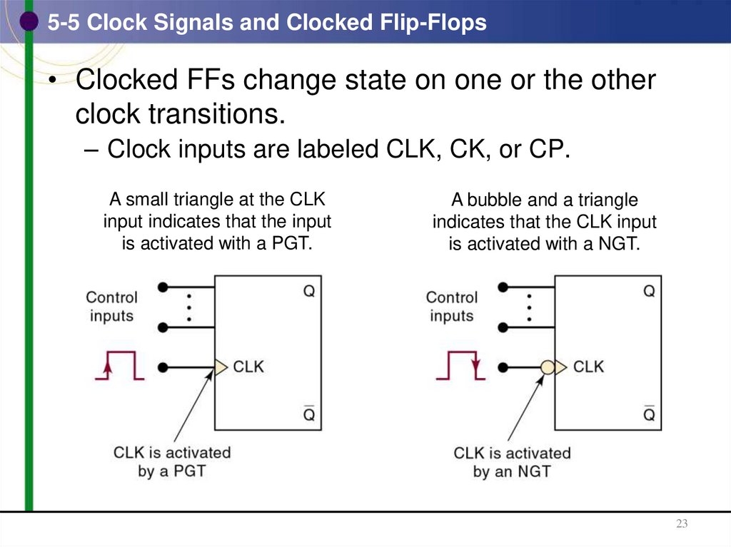
23. 5-5 Clock Signals and Clocked Flip-Flops
• Clocked FFs change state on one or the otherclock transitions.
– Clock inputs are labeled CLK, CK, or CP.
A small triangle at the CLK
input indicates that the input
is activated with a PGT.
A bubble and a triangle
indicates that the CLK input
is activated with a NGT.
23
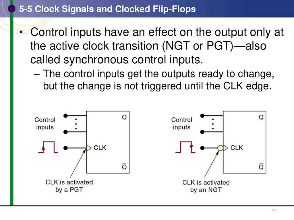
24. 5-5 Clock Signals and Clocked Flip-Flops
• Control inputs have an effect on the output only atthe active clock transition (NGT or PGT)—also
called synchronous control inputs.
– The control inputs get the outputs ready to change,
but the change is not triggered until the CLK edge.
24
25. 5-5 Clock Signals and Clocked Flip-Flops
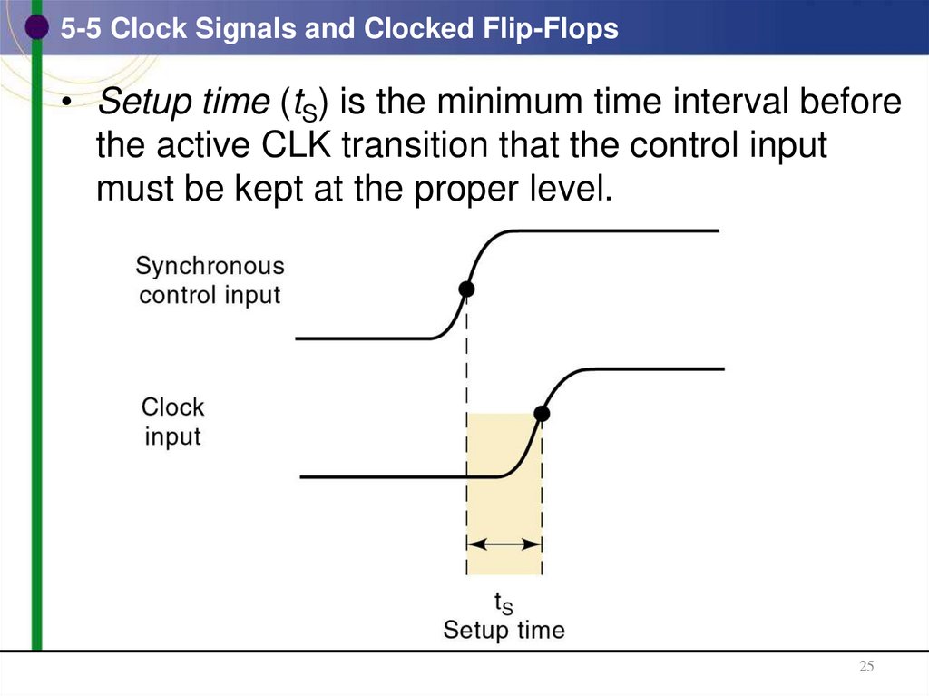
• Setup time (tS) is the minimum time interval beforethe active CLK transition that the control input
must be kept at the proper level.
25
26. 5-5 Clock Signals and Clocked Flip-Flops
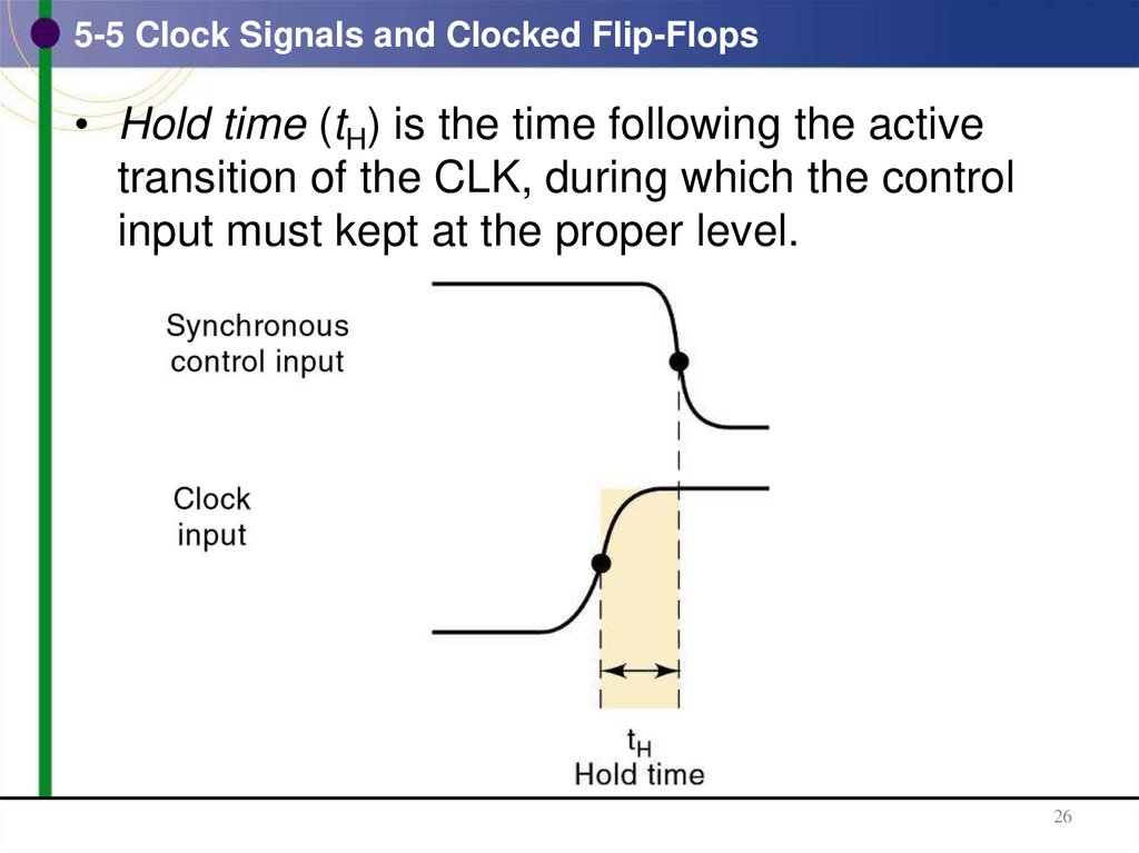
• Hold time (tH) is the time following the activetransition of the CLK, during which the control
input must kept at the proper level.
26
27. 5-6 Clocked S-R Flip-Flop
• The S and R inputs are synchronous controlinputs, which control the state the FF will go to
when the clock pulse occurs.
– The CLK input is the trigger input that causes the
FF to change states according to the S and R inputs.
• SET-RESET (or SET-CLEAR) FF will change
states at positive- or negative-going clock edges.
27
28. 5-6 Clocked S-R Flip-Flop
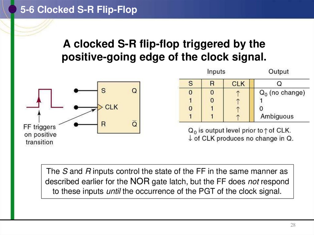
A clocked S-R flip-flop triggered by thepositive-going edge of the clock signal.
The S and R inputs control the state of the FF in the same manner as
described earlier for the NOR gate latch, but the FF does not respond
to these inputs until the occurrence of the PGT of the clock signal.
28
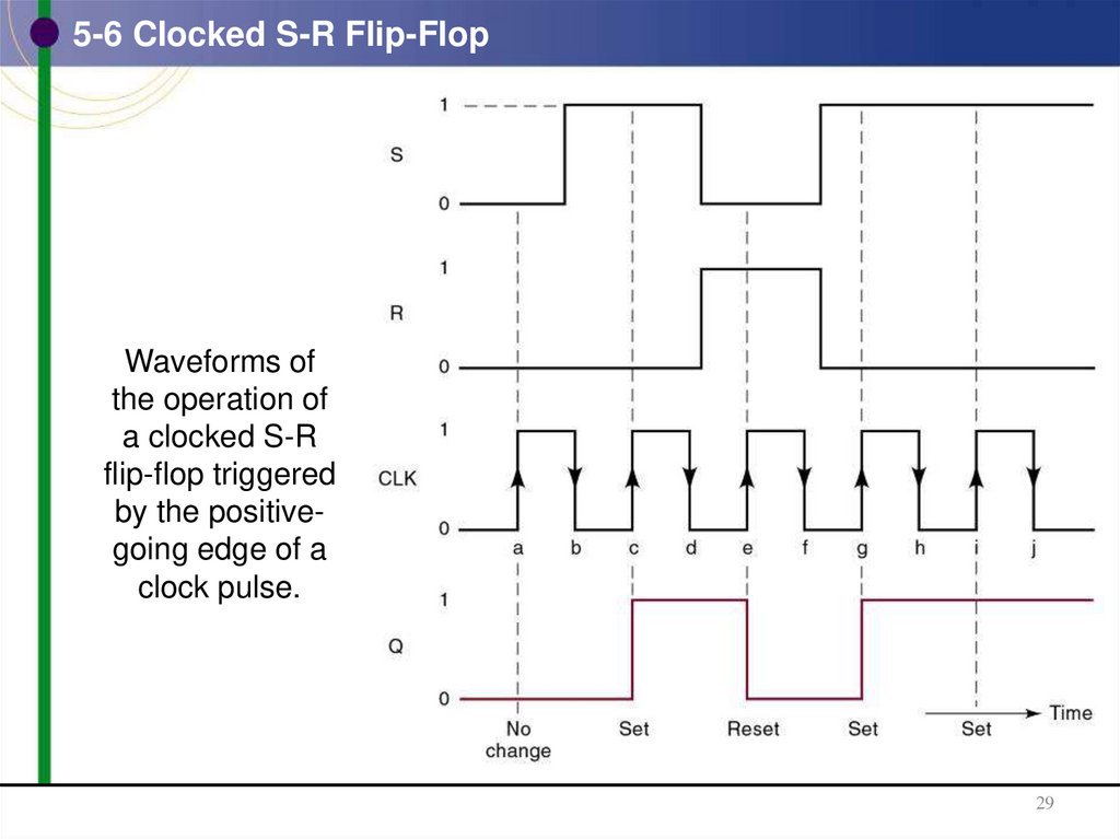
29. 5-6 Clocked S-R Flip-Flop
Waveforms ofthe operation of
a clocked S-R
flip-flop triggered
by the positivegoing edge of a
clock pulse.
29
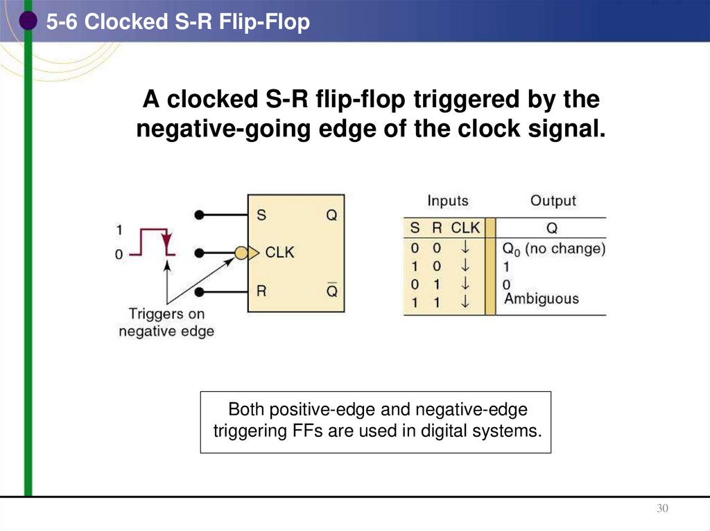
30. 5-6 Clocked S-R Flip-Flop
A clocked S-R flip-flop triggered by thenegative-going edge of the clock signal.
Both positive-edge and negative-edge
triggering FFs are used in digital systems.
30
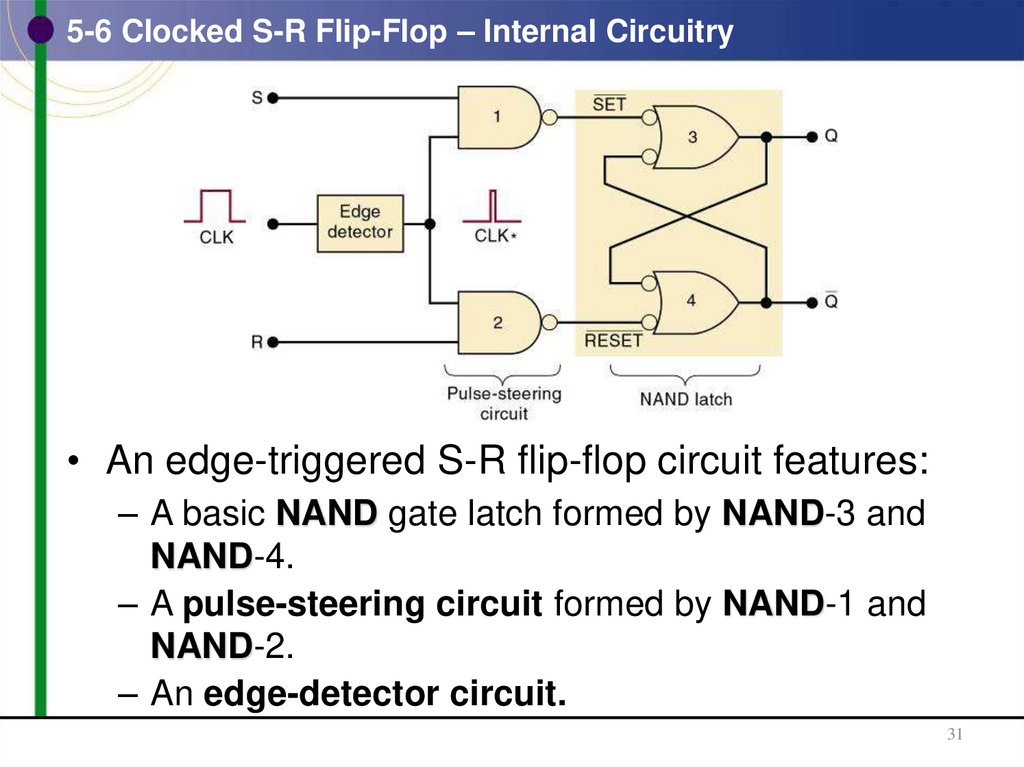
31. 5-6 Clocked S-R Flip-Flop – Internal Circuitry
• An edge-triggered S-R flip-flop circuit features:– A basic NAND gate latch formed by NAND-3 and
NAND-4.
– A pulse-steering circuit formed by NAND-1 and
NAND-2.
– An edge-detector circuit.
31
32. 5-6 Clocked S-R Flip-Flop – Internal Circuitry
• Implementation of edge-detector circuits used inedge-triggered flip-flops:
– (a) PGT; (b) NGT.
The duration of the CLK* pulses is typically 2–5 ns.
32
33. 5-7 Clocked J-K Flip-Flop
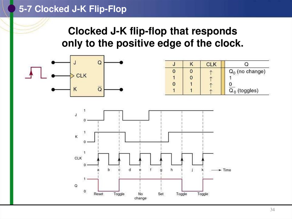
• Operates like the S-R FF.– J is SET, K is CLEAR.
• When J and K are both HIGH, output is toggled
to the opposite state.
– May be positive going or negative going clock trigger.
• Much more versatile than the S-R flip-flop, as it
has no ambiguous states.
– Has the ability to do everything the S-R FF does,
plus operates in toggle mode.
33
34. 5-7 Clocked J-K Flip-Flop
Clocked J-K flip-flop that respondsonly to the positive edge of the clock.
34
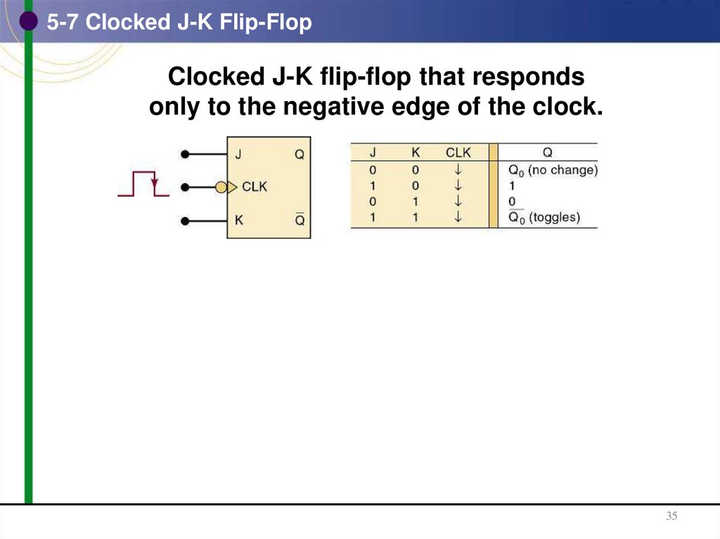
35. 5-7 Clocked J-K Flip-Flop
Clocked J-K flip-flop that respondsonly to the negative edge of the clock.
35
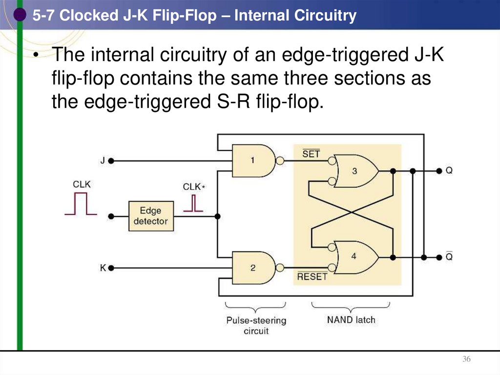
36. 5-7 Clocked J-K Flip-Flop – Internal Circuitry
• The internal circuitry of an edge-triggered J-Kflip-flop contains the same three sections as
the edge-triggered S-R flip-flop.
36
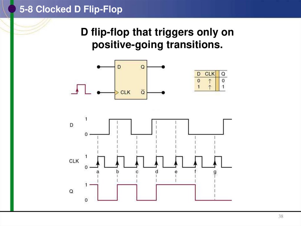
37. 5-8 Clocked D Flip-Flop
• One data input—output changes to the value ofthe input at either the positive- or negative-going
clock trigger.
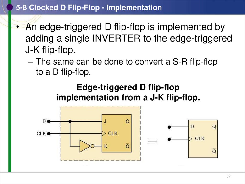
• May be implemented with a J-K FF by tying
the J input to the K input through an inverter.
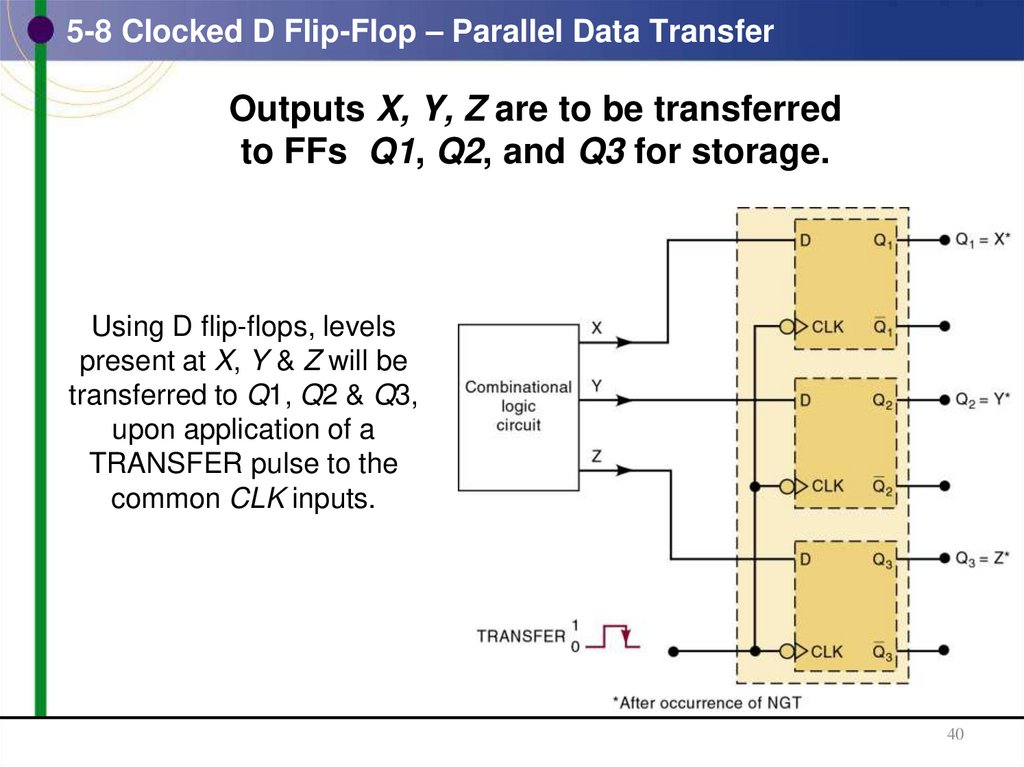
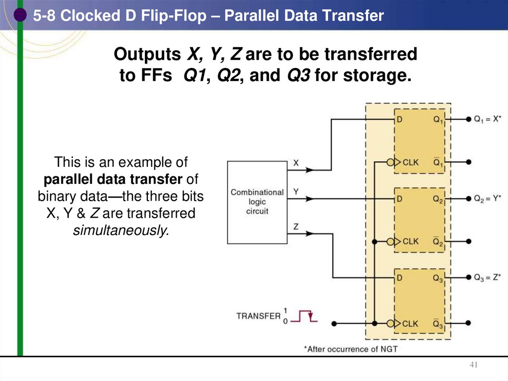
• Useful for parallel data transfer.
37
38. 5-8 Clocked D Flip-Flop
D flip-flop that triggers only onpositive-going transitions.
38
39. 5-8 Clocked D Flip-Flop - Implementation
• An edge-triggered D flip-flop is implemented byadding a single INVERTER to the edge-triggered
J-K flip-flop.
– The same can be done to convert a S-R flip-flop
to a D flip-flop.
Edge-triggered D flip-flop
implementation from a J-K flip-flop.
39
40. 5-8 Clocked D Flip-Flop – Parallel Data Transfer
Outputs X, Y, Z are to be transferredto FFs Q1, Q2, and Q3 for storage.
Using D flip-flops, levels
present at X, Y & Z will be
transferred to Q1, Q2 & Q3,
upon application of a
TRANSFER pulse to the
common CLK inputs.
40
41. 5-8 Clocked D Flip-Flop – Parallel Data Transfer
Outputs X, Y, Z are to be transferredto FFs Q1, Q2, and Q3 for storage.
This is an example of
parallel data transfer of
binary data—the three bits
X, Y & Z are transferred
simultaneously.
41
42. 5-9 D Latch (Transparent Latch)
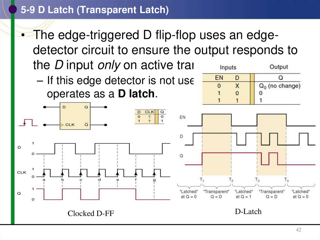
• The edge-triggered D flip-flop uses an edgedetector circuit to ensure the output responds tothe D input only on active transition of the clock.
– If this edge detector is not used, the resultant circuit
operates as a D latch.
Clocked D-FF
D-Latch
42
43. 5-9 D Latch (Transparent Latch)
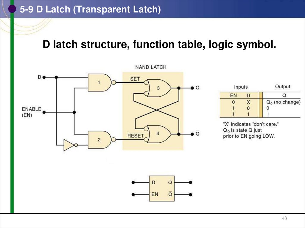
D latch structure, function table, logic symbol.43
44. 5-9 D Latch (Transparent Latch)
• The circuit contains the NAND latch and thesteering NAND gates 1 and 2 without the edgedetector circuit.
• The common input to the steering gates is called
an enable input (abbreviated EN)—rather than a
clock input.
– Its effect on the Q and Q outputs is not restricted to
occurring only on its transitions
44
45. 5-10 Asynchronous Inputs
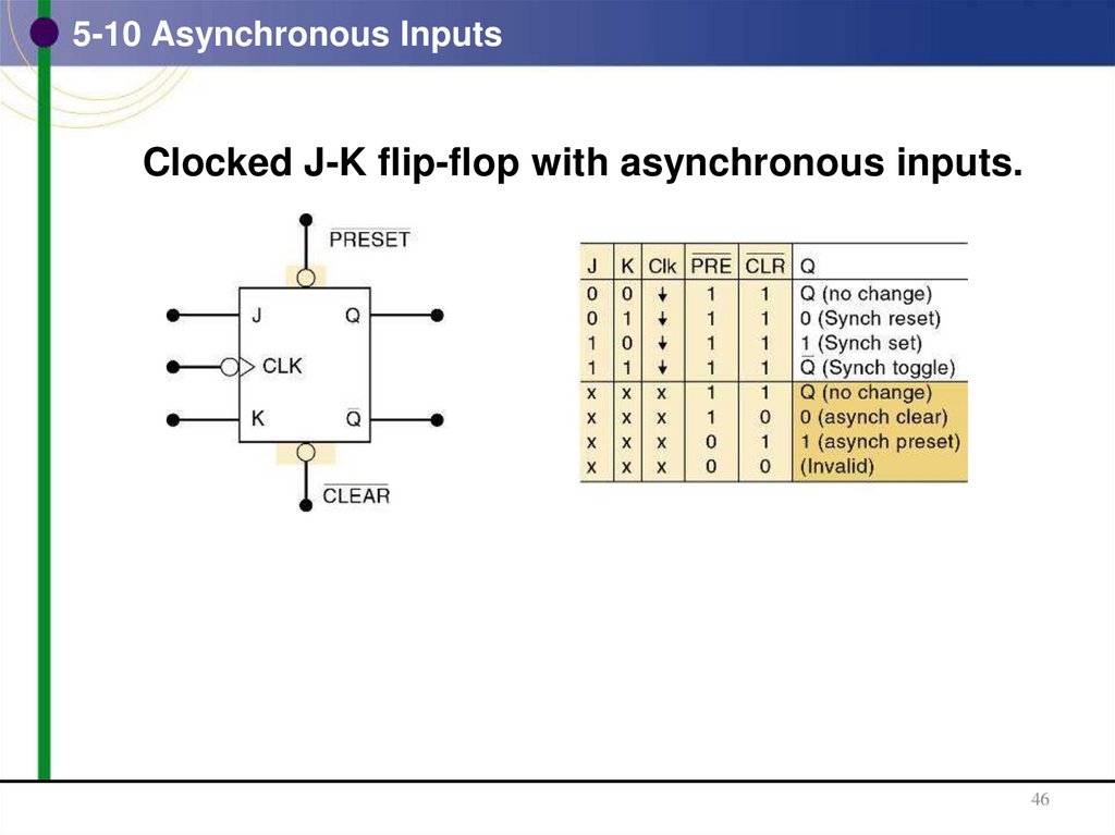
• Inputs that depend on the clock are synchronous.• Most clocked FFs have asynchronous inputs that
do not depend on the clock.
– Labels PRE & CLR are used for asynchronous inputs.
• Active-LOW asynchronous inputs will have a bar
over the labels and inversion bubbles.
• If the asynchronous inputs are not used they will
be tied to their inactive state.
45
46. 5-10 Asynchronous Inputs
Clocked J-K flip-flop with asynchronous inputs.46
47. 5-10 Asynchronous Inputs - Designations
• IC manufacturers do not agree on nomenclaturefor asynchronous inputs.
– The most common designations are PRE (PRESET)
and CLR (CLEAR).
• Clearly distinguished from synchronous SET & RESET.
– Labels such as S-D (direct SET) and R-D (direct
RESET) are also used.
47
48. 5-10 Asynchronous Inputs
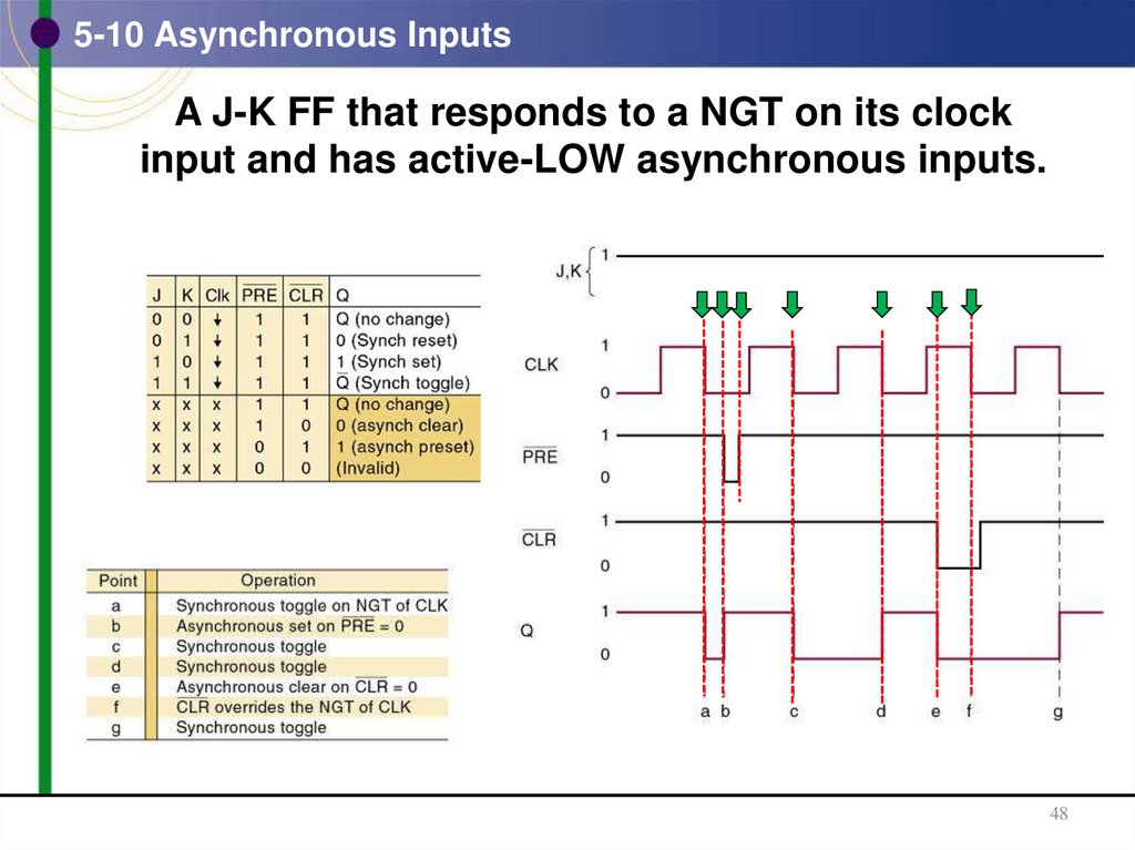
A J-K FF that responds to a NGT on its clockinput and has active-LOW asynchronous inputs.
48
49. 5-11 Flip-Flop Timing Considerations - Parameters
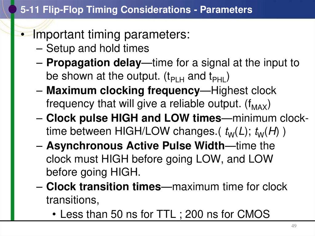
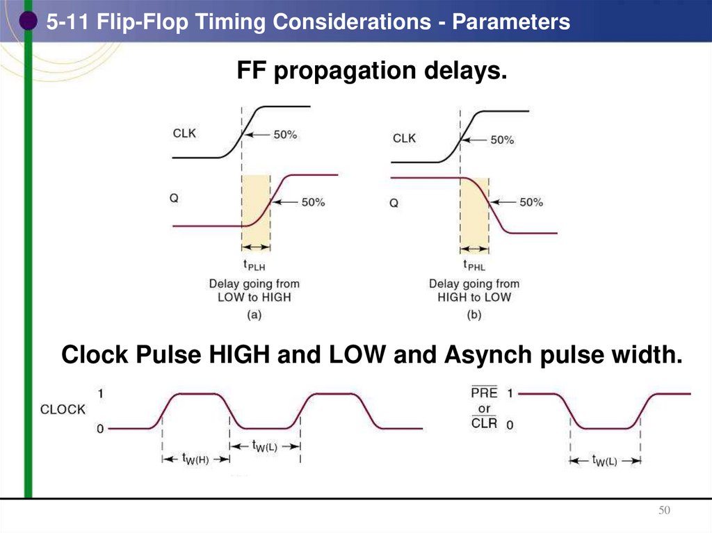
• Important timing parameters:– Setup and hold times
– Propagation delay—time for a signal at the input to
be shown at the output. (tPLH and tPHL)
– Maximum clocking frequency—Highest clock
frequency that will give a reliable output. (fMAX)
– Clock pulse HIGH and LOW times—minimum clocktime between HIGH/LOW changes.( tW(L); tW(H) )
– Asynchronous Active Pulse Width—time the
clock must HIGH before going LOW, and LOW
before going HIGH.
– Clock transition times—maximum time for clock
transitions,
• Less than 50 ns for TTL ; 200 ns for CMOS
49
50. 5-11 Flip-Flop Timing Considerations - Parameters
FF propagation delays.Clock Pulse HIGH and LOW and Asynch pulse width.
50
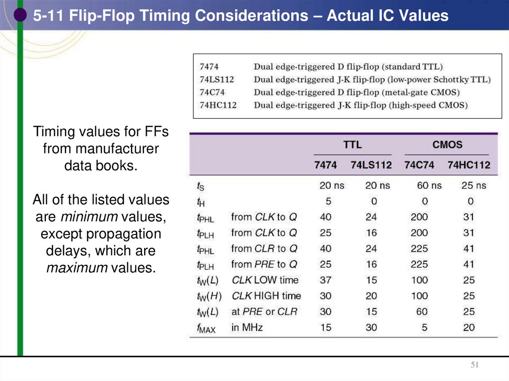
51. 5-11 Flip-Flop Timing Considerations – Actual IC Values
Timing values for FFsfrom manufacturer
data books.
All of the listed values
are minimum values,
except propagation
delays, which are
maximum values.
51
52. Example
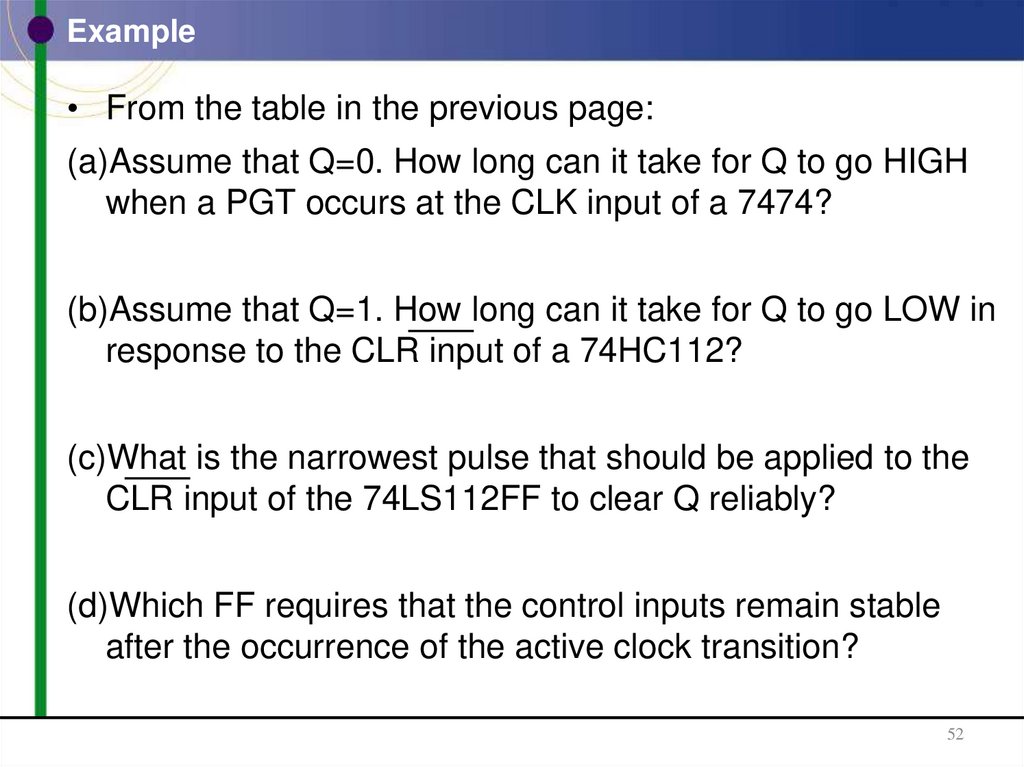
• From the table in the previous page:(a)Assume that Q=0. How long can it take for Q to go HIGH
when a PGT occurs at the CLK input of a 7474?
(b)Assume that Q=1. How long can it take for Q to go LOW in
response to the CLR input of a 74HC112?
(c)What is the narrowest pulse that should be applied to the
CLR input of the 74LS112FF to clear Q reliably?
(d)Which FF requires that the control inputs remain stable
after the occurrence of the active clock transition?
52
53. 5-12 Potential Timing Problems in FF Circuits
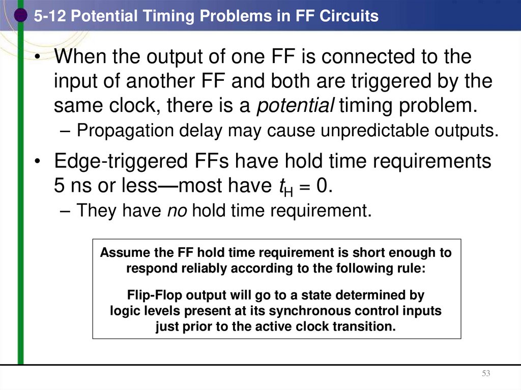
• When the output of one FF is connected to theinput of another FF and both are triggered by the
same clock, there is a potential timing problem.
– Propagation delay may cause unpredictable outputs.
• Edge-triggered FFs have hold time requirements
5 ns or less—most have tH = 0.
– They have no hold time requirement.
Assume the FF hold time requirement is short enough to
respond reliably according to the following rule:
Flip-Flop output will go to a state determined by
logic levels present at its synchronous control inputs
just prior to the active clock transition.
53
54. 5-12 Potential Timing Problems in FF Circuits
Q2 will respond properlyto the level present at
Q1 prior to NGT of CLK—
provided Q2 ’s hold time
requirement, tH, is less than
Q1’s propagation delay.
54
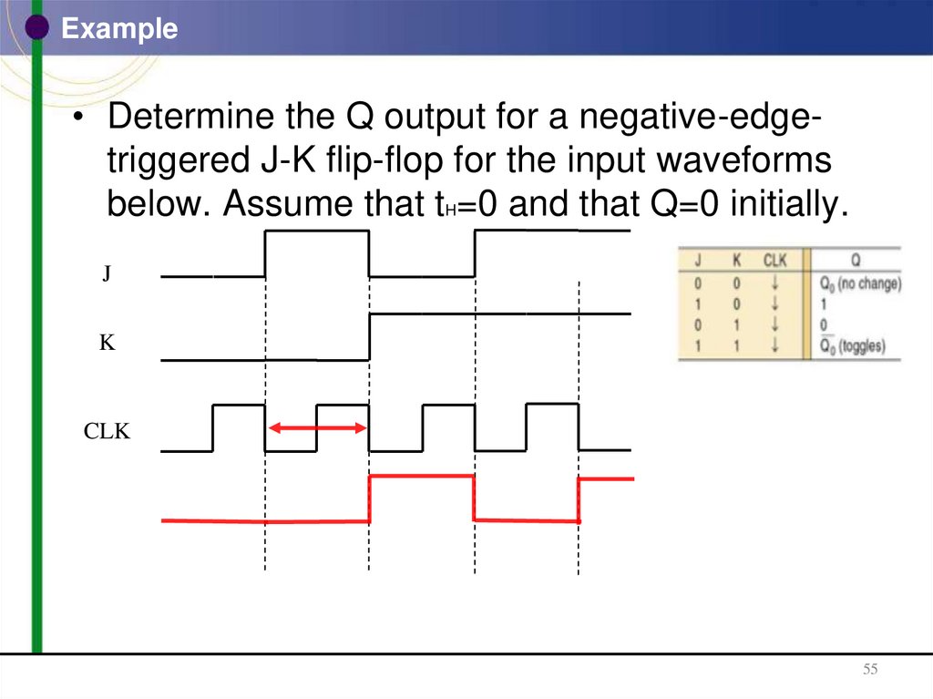
55. Example
• Determine the Q output for a negative-edgetriggered J-K flip-flop for the input waveformsbelow. Assume that tH=0 and that Q=0 initially.
J
K
CLK
55
56. 5-13 Flip-Flop Applications
• Examples of applications:– Counting; Storing binary data
– Transferring binary data between locations
• Many FF applications are categorized sequential.
– Output follows a predetermined sequence of states.
56
57. 5-14 Flip-Flop Synchronization
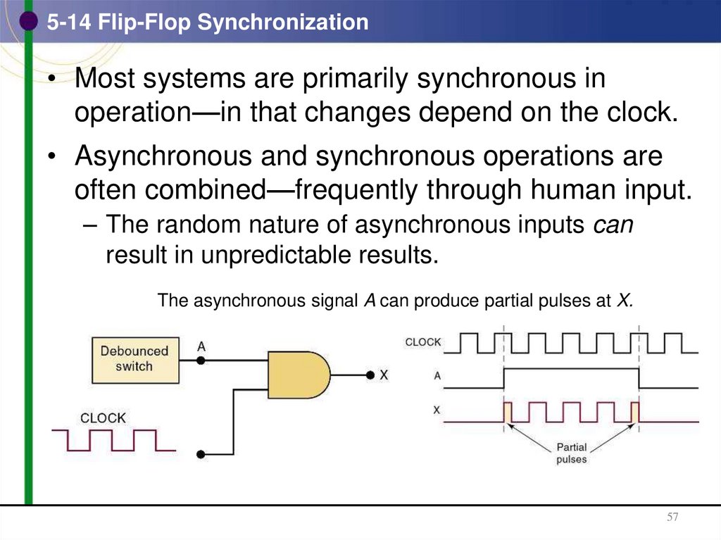
• Most systems are primarily synchronous inoperation—in that changes depend on the clock.
• Asynchronous and synchronous operations are
often combined—frequently through human input.
– The random nature of asynchronous inputs can
result in unpredictable results.
The asynchronous signal A can produce partial pulses at X.
57
58. 5-14 Flip-Flop Synchronization
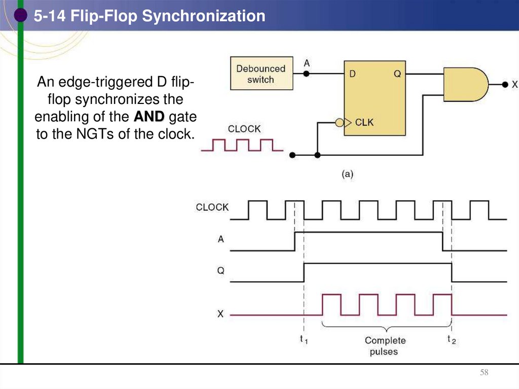
An edge-triggered D flipflop synchronizes theenabling of the AND gate
to the NGTs of the clock.
58
59. 5-15 Detecting an Input Sequence
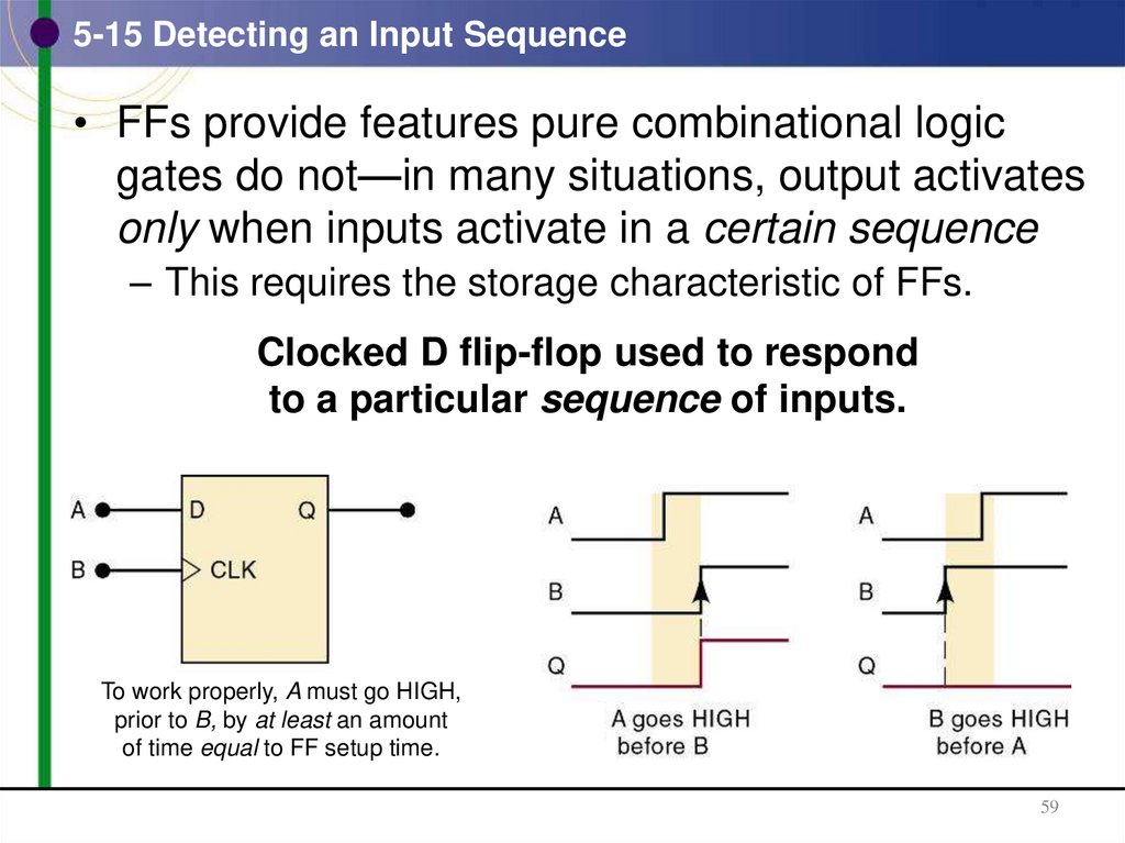
• FFs provide features pure combinational logicgates do not—in many situations, output activates
only when inputs activate in a certain sequence
– This requires the storage characteristic of FFs.
Clocked D flip-flop used to respond
to a particular sequence of inputs.
To work properly, A must go HIGH,
prior to B, by at least an amount
of time equal to FF setup time.
59
60. 5-16 Data Storage and Transfer
• FFs are commonly used for storage and transferof binary data.
– Groups used for storage are registers.
• Data transfers take place when data is moved
between registers or FFs.
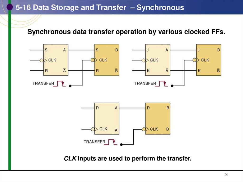
– Synchronous transfers take place at clock PGT/NGT.
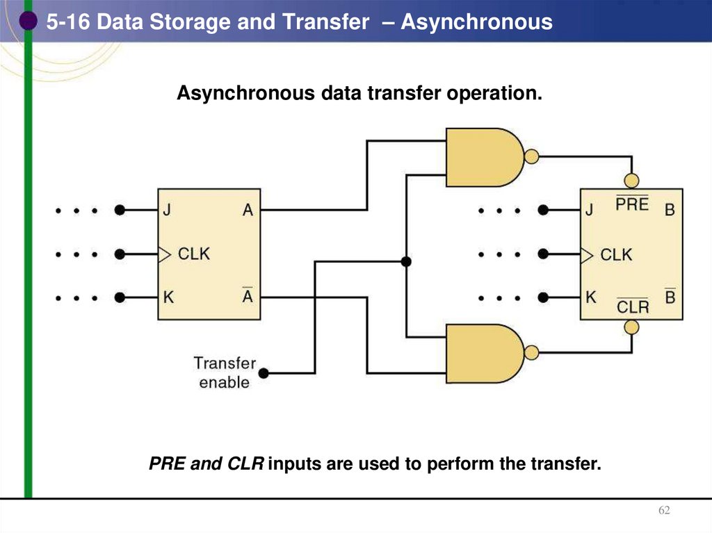
– Asynchronous transfers are controlled by PRE & CLR.
60
61. 5-16 Data Storage and Transfer – Synchronous
Synchronous data transfer operation by various clocked FFs.CLK inputs are used to perform the transfer.
61
62. 5-16 Data Storage and Transfer – Asynchronous
Asynchronous data transfer operation.PRE and CLR inputs are used to perform the transfer.
62
63. 5-16 Data Storage and Transfer – Parallel
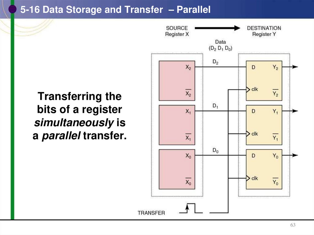
Transferring thebits of a register
simultaneously is
a parallel transfer.
63
64. 5-17 Serial Data Transfer
• Transferring the bits of a register a bit at a time isa serial transfer.
64
65. 5-17 Serial Data Transfer – Shift Register
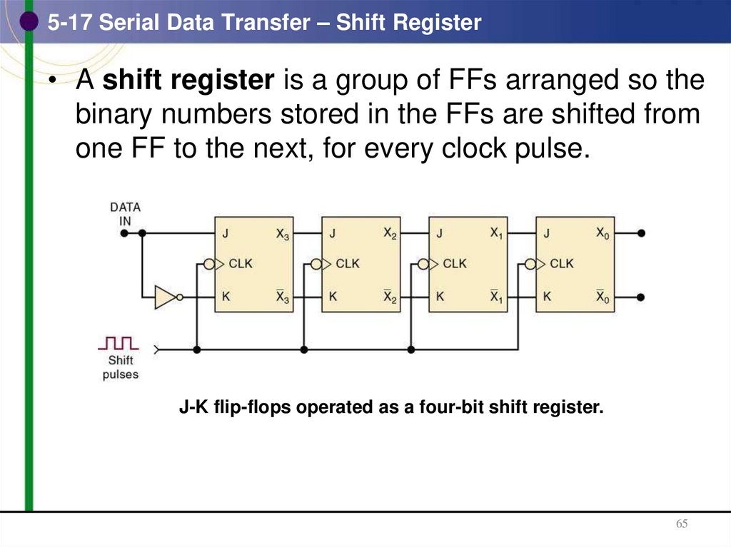
• A shift register is a group of FFs arranged so thebinary numbers stored in the FFs are shifted from
one FF to the next, for every clock pulse.
J-K flip-flops operated as a four-bit shift register.
65
66. 5-17 Serial Data Transfer – Shift Register
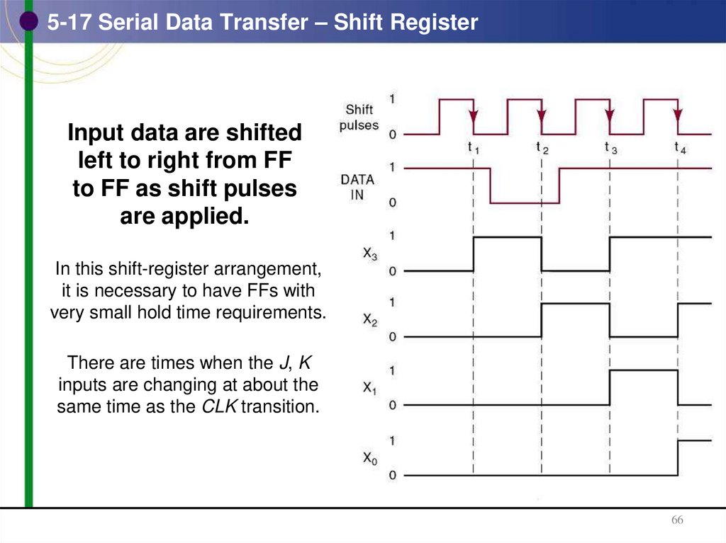
Input data are shiftedleft to right from FF
to FF as shift pulses
are applied.
In this shift-register arrangement,
it is necessary to have FFs with
very small hold time requirements.
There are times when the J, K
inputs are changing at about the
same time as the CLK transition.
66
67. 5-17 Serial Data Transfer – Shift Register
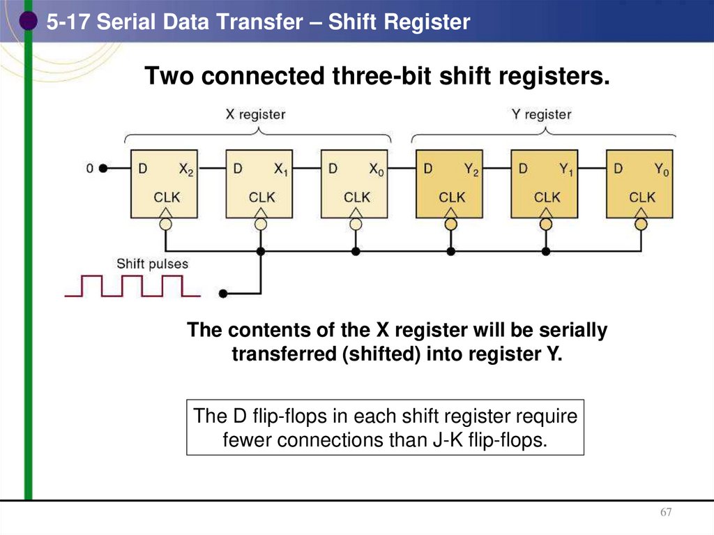
Two connected three-bit shift registers.The contents of the X register will be serially
transferred (shifted) into register Y.
The D flip-flops in each shift register require
fewer connections than J-K flip-flops.
67
68. 5-17 Serial Data Transfer – Shift Register
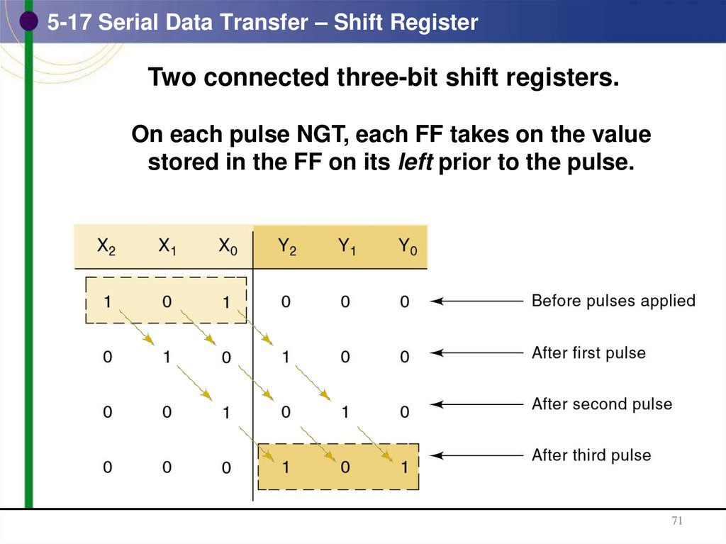
Two connected three-bit shift registers.The complete transfer of the three bits
of data requires three shift pulses.
68
69. 5-17 Serial Data Transfer – Shift Register
Two connected three-bit shift registers.On each pulse NGT, each FF takes on the value
stored in the FF on its left prior to the pulse.
69
70. 5-17 Serial Data Transfer – Shift Register
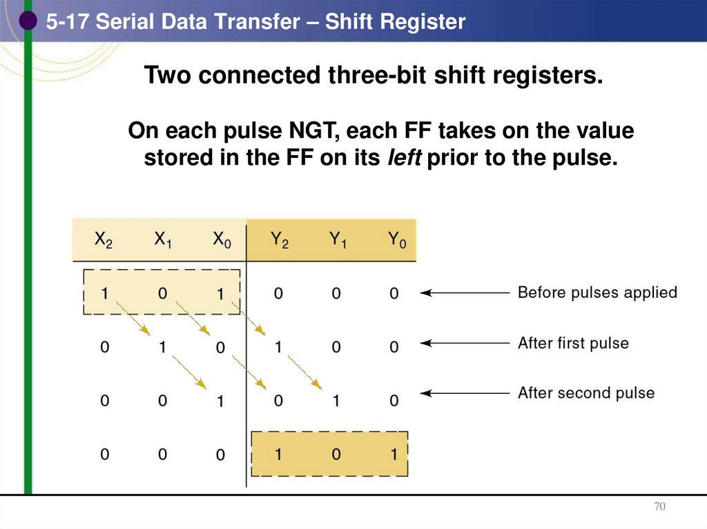
Two connected three-bit shift registers.On each pulse NGT, each FF takes on the value
stored in the FF on its left prior to the pulse.
70
71. 5-17 Serial Data Transfer – Shift Register
Two connected three-bit shift registers.On each pulse NGT, each FF takes on the value
stored in the FF on its left prior to the pulse.
71
72. 5-17 Serial Data Transfer – Shift Register
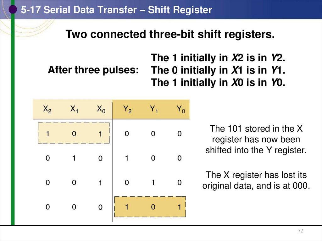
Two connected three-bit shift registers.After three pulses:
The 1 initially in X2 is in Y2.
The 0 initially in X1 is in Y1.
The 1 initially in X0 is in Y0.
The 101 stored in the X
register has now been
shifted into the Y register.
The X register has lost its
original data, and is at 000.
72
73. 5-17 Serial Data Transfer vs. Parallel
• FFs can just as easily be connected so thatinformation shifts from right to left.
– No general advantage of one direction over another.
• Often dictated by the nature of the application.
• Parallel transfer requires more interconnections
between sending & receiving registers than serial.
– More critical when a greater number of bits of are
being transferred.
• Often, a combination of types is used
– Taking advantage of parallel transfer speed and serial
transfer the economy and simplicity of serial transfer.
73
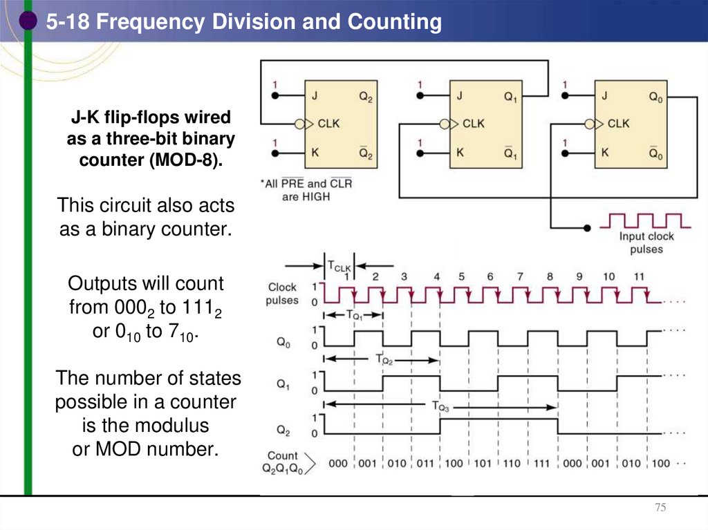
74. 5-18 Frequency Division and Counting
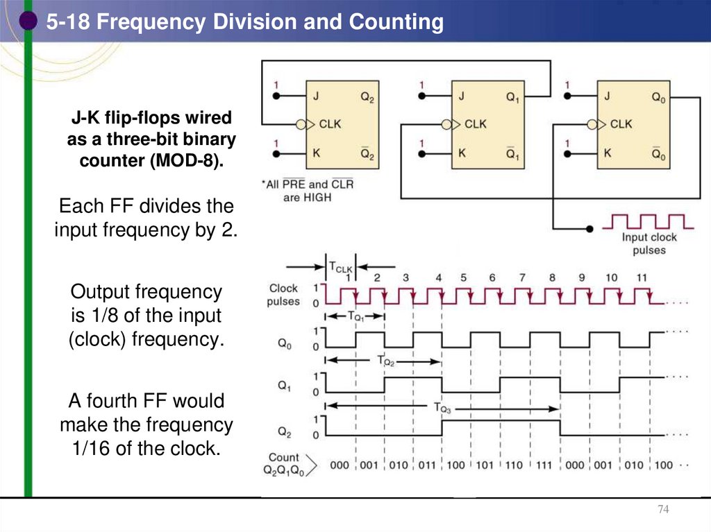
J-K flip-flops wiredas a three-bit binary
counter (MOD-8).
Each FF divides the
input frequency by 2.
Output frequency
is 1/8 of the input
(clock) frequency.
A fourth FF would
make the frequency
1/16 of the clock.
74
75. 5-18 Frequency Division and Counting
J-K flip-flops wiredas a three-bit binary
counter (MOD-8).
This circuit also acts
as a binary counter.
Outputs will count
from 0002 to 1112
or 010 to 710.
The number of states
possible in a counter
is the modulus
or MOD number.
75
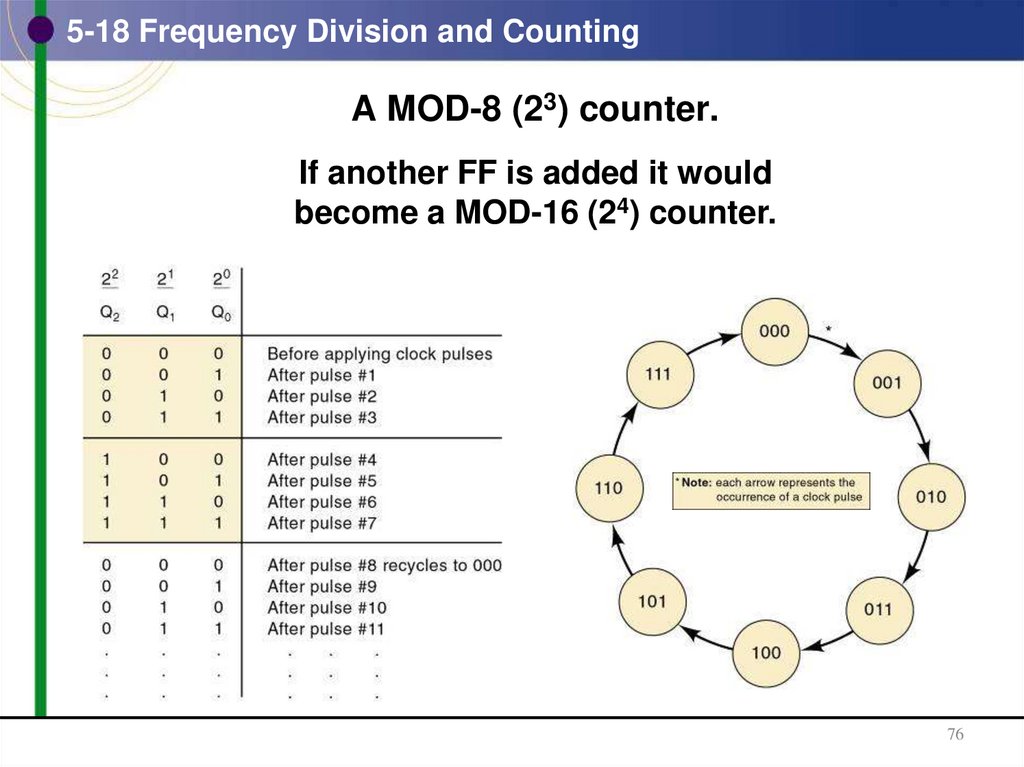
76. 5-18 Frequency Division and Counting
A MOD-8 (23) counter.If another FF is added it would
become a MOD-16 (24) counter.
76
77. 5-19 Microcomputer Application
• Microprocessor units (MPUs) perform manyfunctions involving use of registers for data
transfer and storage.
• MPUs may send data to external registers
for many purposes, including:
– Solenoid/relay control; Device positioning.
– Motor starting & speed controls.
77
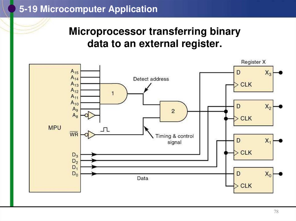
78. 5-19 Microcomputer Application
Microprocessor transferring binarydata to an external register.
78
79. 5-20 Schmitt-Trigger Devices
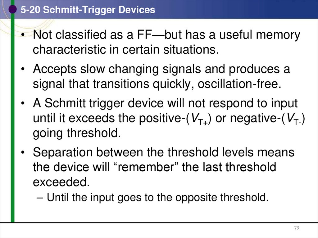
• Not classified as a FF—but has a useful memorycharacteristic in certain situations.
• Accepts slow changing signals and produces a
signal that transitions quickly, oscillation-free.
• A Schmitt trigger device will not respond to input
until it exceeds the positive-(VT+) or negative-(VT-)
going threshold.
• Separation between the threshold levels means
the device will “remember” the last threshold
exceeded.
– Until the input goes to the opposite threshold.
79
80. 5-20 Schmitt-Trigger Devices
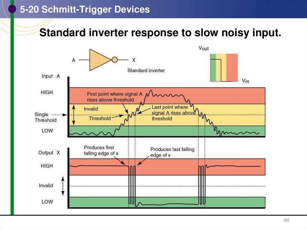
Standard inverter response to slow noisy input.80
81. 5-20 Schmitt-Trigger Devices
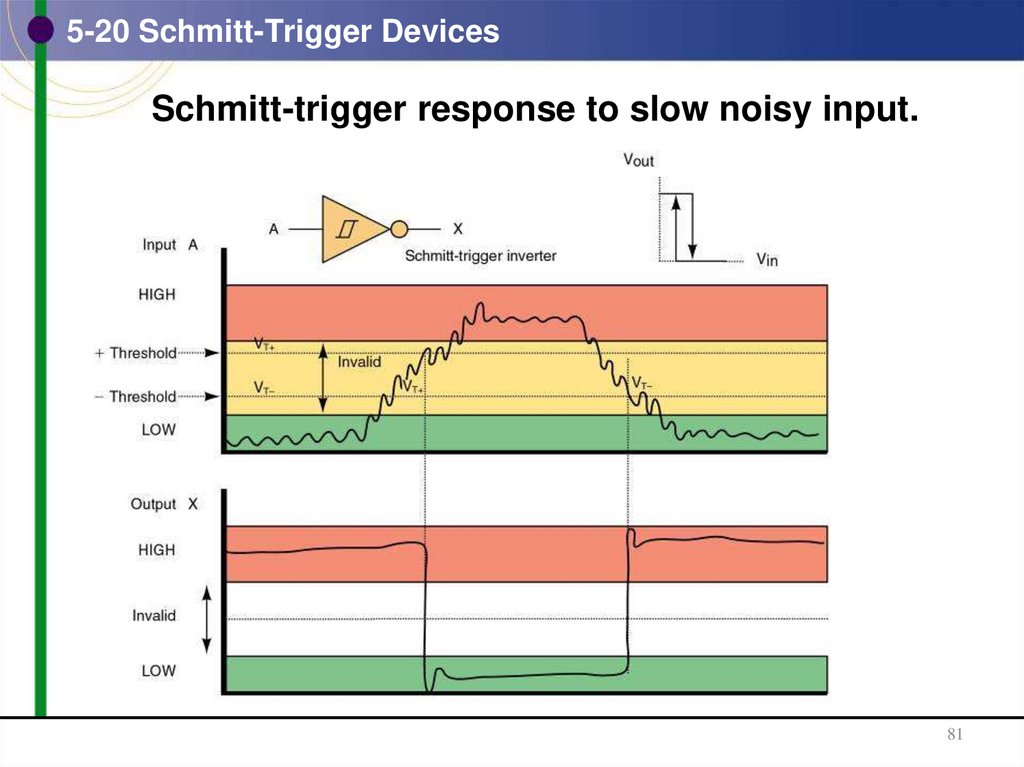
Schmitt-trigger response to slow noisy input.81
82. 5-21 One-shot (Monostable Multivibrator)
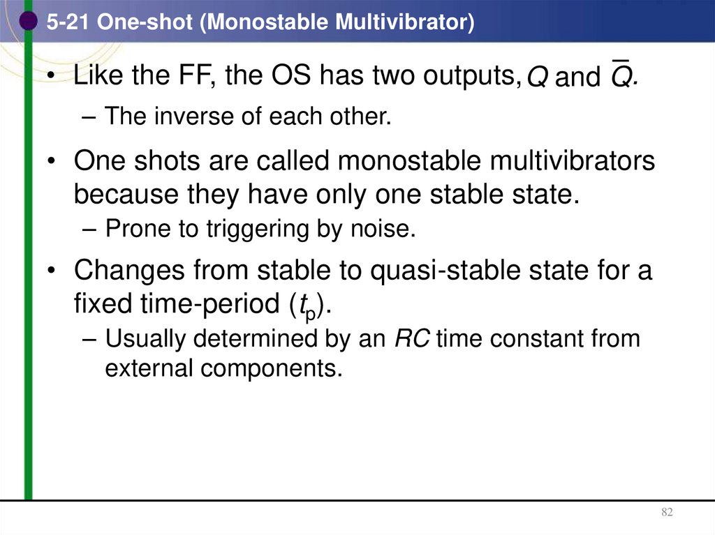
• Like the FF, the OS has two outputs, Q and Q.– The inverse of each other.
• One shots are called monostable multivibrators
because they have only one stable state.
– Prone to triggering by noise.
• Changes from stable to quasi-stable state for a
fixed time-period (tp).
– Usually determined by an RC time constant from
external components.
82
83. 5-21 One-shot (Monostable Multivibrator)
• Nonretriggerable devices trigger & return tostable.
• Retriggerable devices can be triggered while in
the quasi-stable state, to begin another pulse.
83
84. 5-21 One-shot (Monostable Multivibrator)
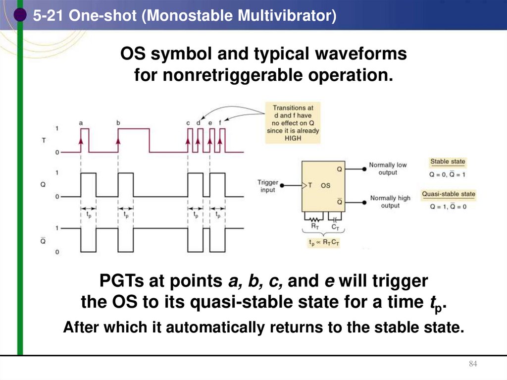
OS symbol and typical waveformsfor nonretriggerable operation.
PGTs at points a, b, c, and e will trigger
the OS to its quasi-stable state for a time tp.
After which it automatically returns to the stable state.
84
85. 5-21 One-shot (Monostable Multivibrator)
OS symbol and typical waveformsfor nonretriggerable operation.
PGTs at points d and f have no effect on the OS
because it has already been triggered quasi-stable.
OS must return to the stable before it can be triggered.
85
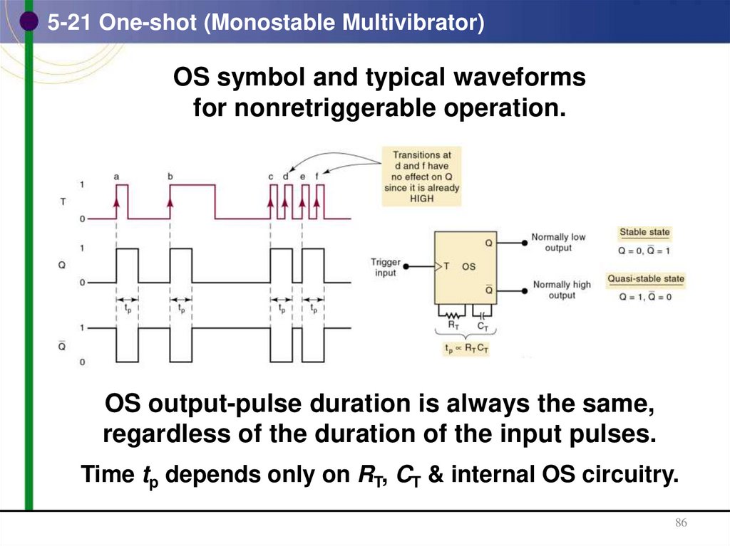
86. 5-21 One-shot (Monostable Multivibrator)
OS symbol and typical waveformsfor nonretriggerable operation.
OS output-pulse duration is always the same,
regardless of the duration of the input pulses.
Time tp depends only on RT, CT & internal OS circuitry.
86
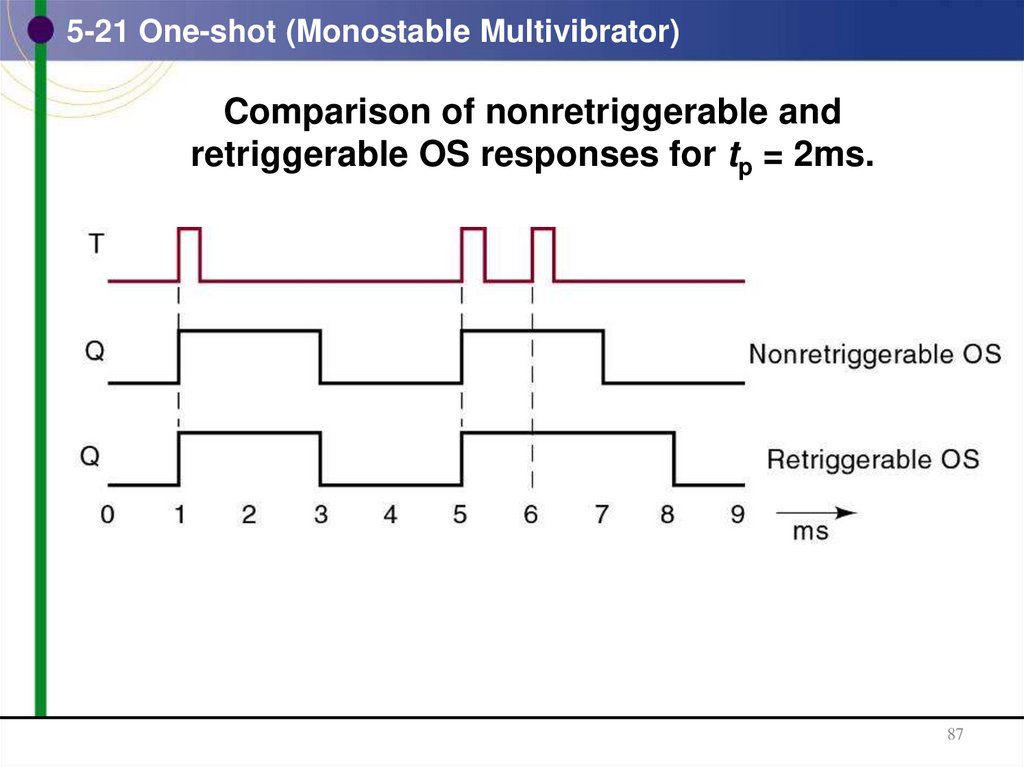
87. 5-21 One-shot (Monostable Multivibrator)
Comparison of nonretriggerable andretriggerable OS responses for tp = 2ms.
87
88. 5-21 One-shot (Monostable Multivibrator)
Retriggerable OS begins a new tp intervaleach time it receives a trigger pulse.
88
89. 5-21 One-shot (Monostable Multivibrator)
74121 nonretriggerable one-shot IC.Contains internal logic gates
to allow inputs A1 , A2 , and B
to trigger OS.
Input B is a Schmitt-trigger—
allowed to have slow transition
times & still reliably trigger OS.
Pins RINT, REXT/CINT, , and CEXT
connect to an external resistor
& capacitor to achieve desired
output pulse duration.
89
90. 5-22 Clock Generator Circuits
• A third type multivibrator has no stable states—anastable or free-running multivibrator.
– Astable or free-running multivibrators switch back
and forth between two unstable states.
– Useful for generating clock signals for synchronous
circuits.
90
91. 5-22 Clock Generator Circuits
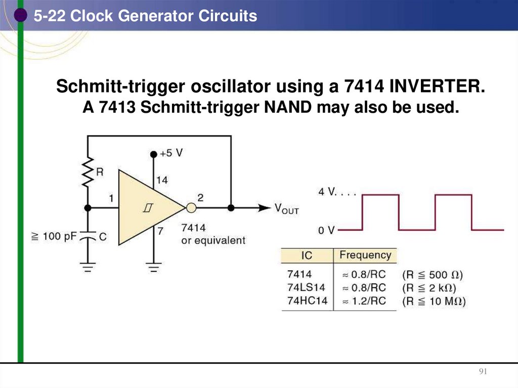
Schmitt-trigger oscillator using a 7414 INVERTER.A 7413 Schmitt-trigger NAND may also be used.
91
92. 5-22 Clock Generator Circuits
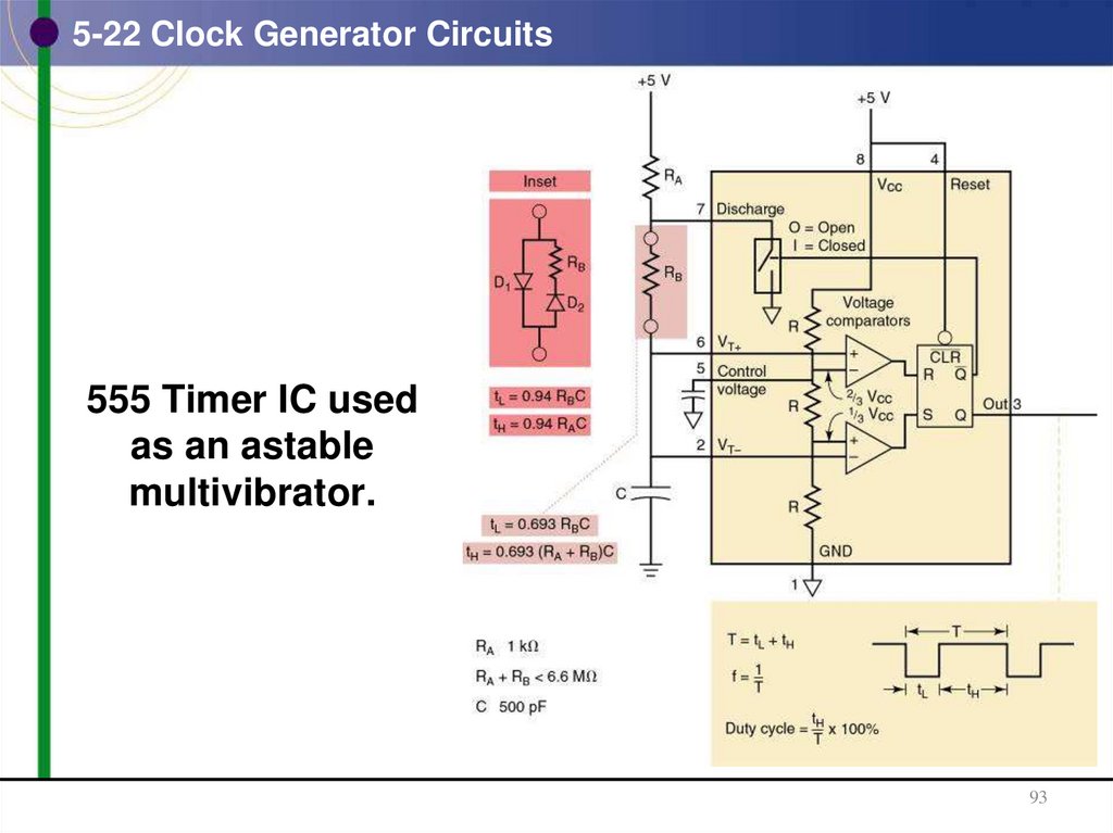
• The 555 timer IC is a TTL-compatible device thatcan operate in several different modes.
– Output is a repetitive rectangular waveform that
switches between two logic levels.
– The time intervals at each logic level are determined
by the R and C values.
• The heart of the 555 timer is two voltage
comparators and an S-R latch.
– The comparators produce a HIGH out when voltage
on the (+) input is greater than on the (-) input.
92
93. 5-22 Clock Generator Circuits
555 Timer IC usedas an astable
multivibrator.
93
94. 5-22 Clock Generator Circuits
• Crystal control may be used if a very stable clockis needed—used in microprocessor systems and
microcomputers where accurate timing intervals
are essential.
94
95. 5-23 Troubleshooting Flip-Flop Circuits
• FFs are subject to the same faults that occur incombinational logic circuits.
– Timing problems create some faults and symptoms
that are not seen in combinational logic circuits.
• Unconnected or floating inputs are particularly
susceptible spurious voltage fluctuations—noise.
• Given sufficient noise amplitude and duration,
logic circuit output may change states in response.
– In a logic gate, output will return to its original state
when the noise signal subsides.
– In a FF, output will remain in its new state due to its
memory characteristic.
95
96. 5-23 Troubleshooting Flip-Flop Circuits
Clock skew occurs when CLK signals arrive
at different FFs at different times.
–
The fault may be seen only intermittently, or
may disappear during testing.
96
97. 5-23 Troubleshooting Flip-Flop Circuits
Extra gating circuits can cause clock skew.97
98. 5-23 Troubleshooting Flip-Flop Circuits
Extra gating circuits can cause clock skew.98















 Электроника


