

 Электроника
Похожие презентации:


")

")


Flip-Flops and Registers Lecture 9 Digital Electronics
1.
Flip-Flops and RegistersLecture 9
Digital Electronics
2.
Course MaterialsAll needed Software and course materials will
be located on Canvas.
◻ Materials that are used in this slides are taken
from the textbook “Digital Electronics A
Practical Approach with VHDL” by William
Kleitz
◻
3.
Flip-Flops and Registerscombination of gates - combinational logic
◻ sequential logic - deal with data storage
circuitry
◻
◻ latch on to (remember) a digital state (1 or 0)
◻ control(s/led by) other circuitry in a specific
sequence
◻ dictated by control clock or enable/disable signals
◻
latch will sometimes have an enable input
◻ used to control the latch to accept or ignore input
states
◻
more sophisticated flip-flops use a clock
4.
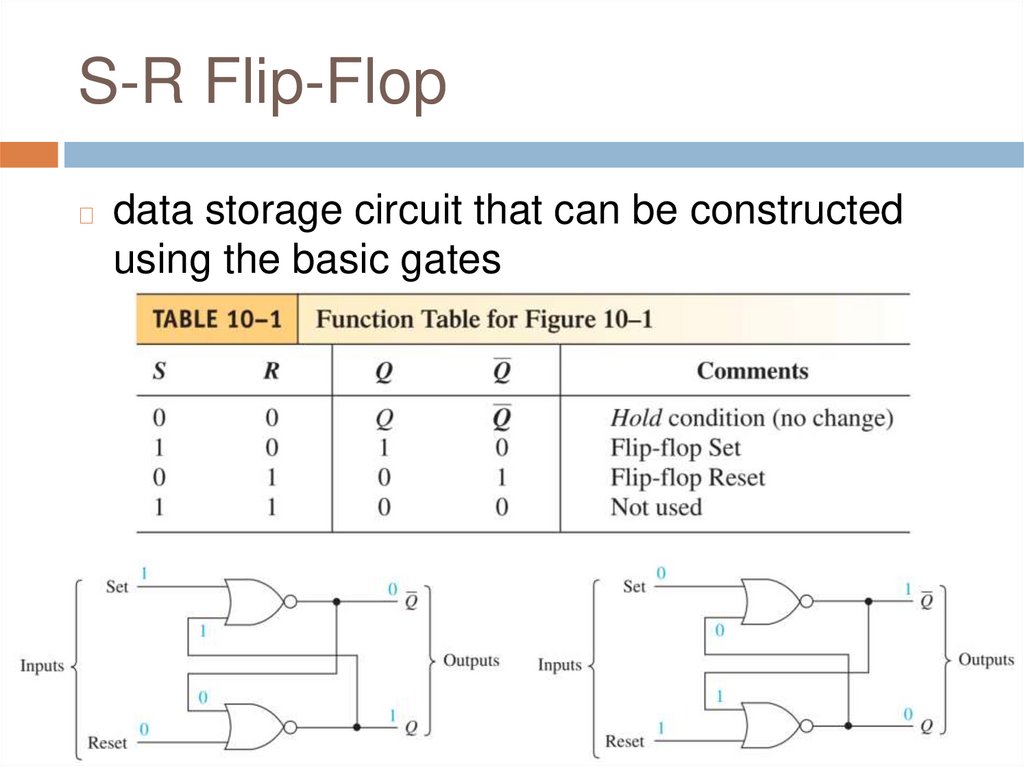
S-R Flip-Flop◻
data storage circuit that can be constructed
using the basic gates
5.
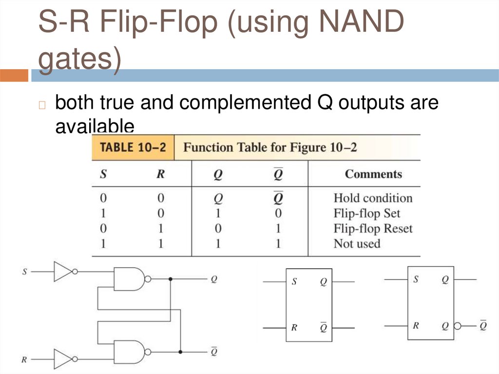
S-R Flip-Flop (using NANDgates)
◻
both true and complemented Q outputs are
available
6.
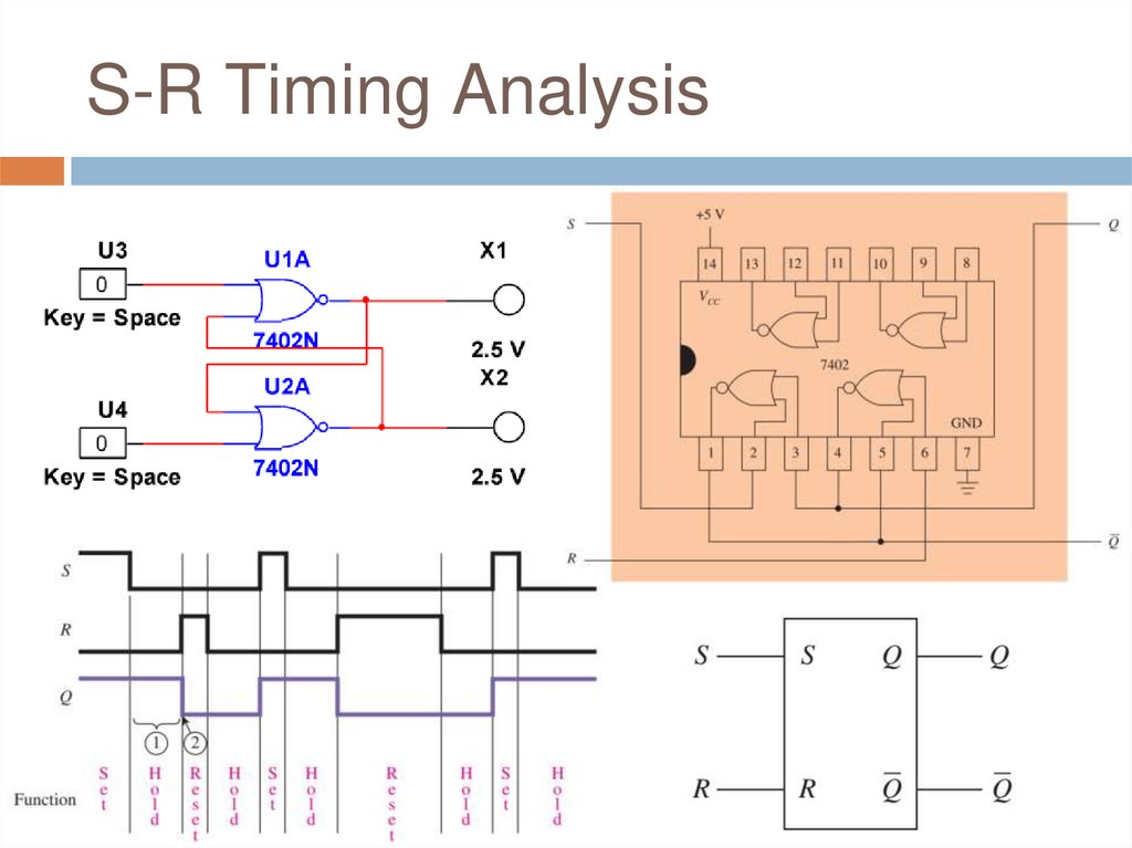
S-R Timing Analysis7.
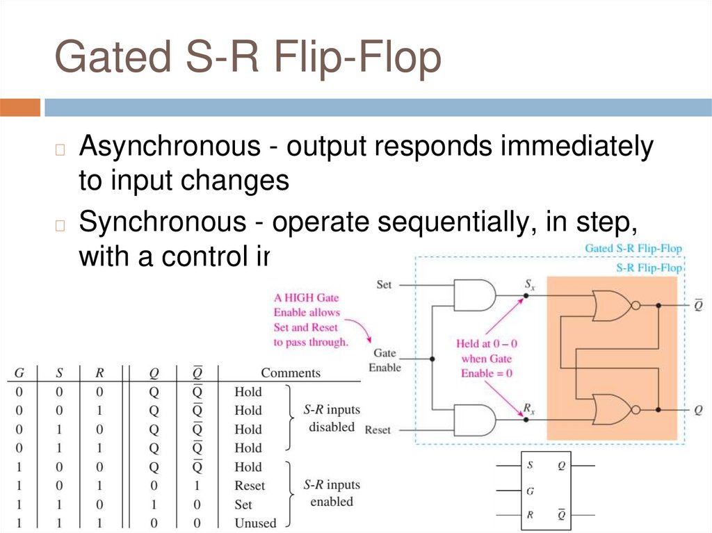
Gated S-R Flip-FlopAsynchronous - output responds immediately
to input changes
◻ Synchronous - operate sequentially, in step,
with a control input
◻
8.
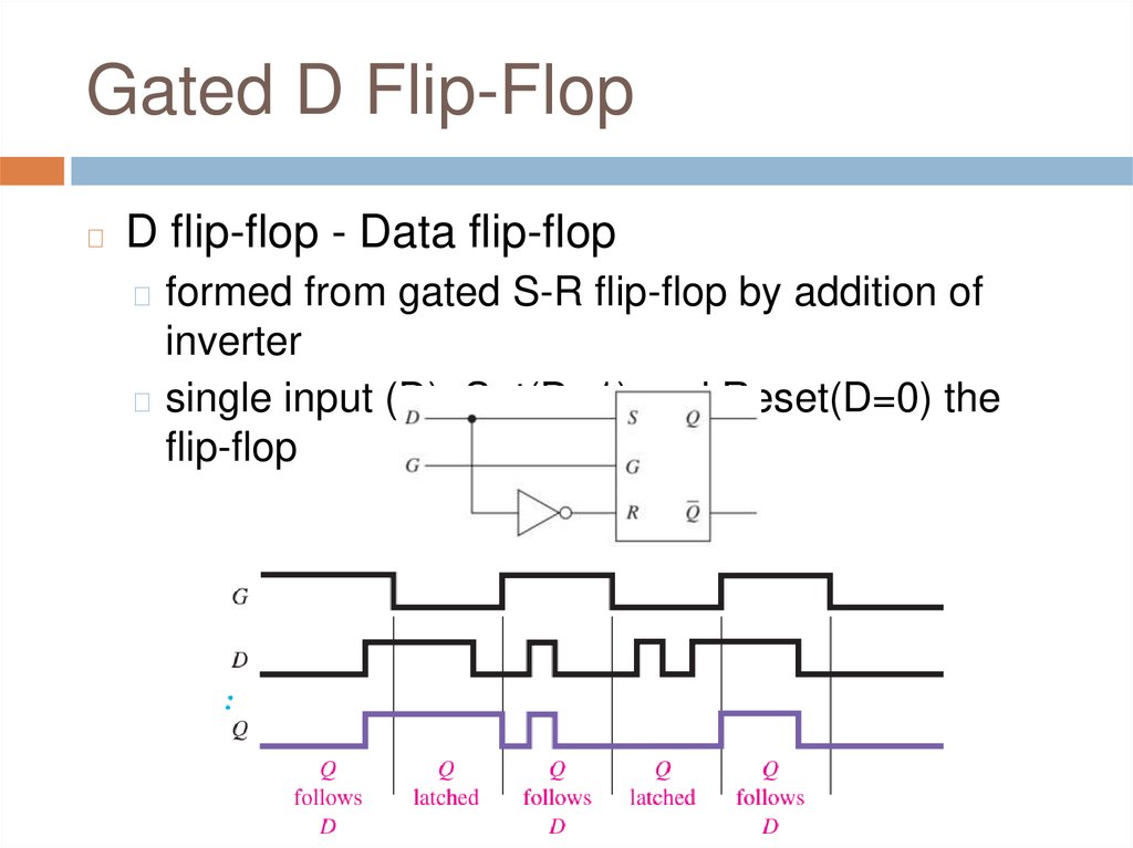
Gated D Flip-Flop◻
D flip-flop - Data flip-flop
◻ formed from gated S-R flip-flop by addition of
inverter
◻ single input (D), Set(D=1) and Reset(D=0) the
flip-flop
9.
Review Questions1.
2.
3.
4.
A flip-flop is different from a basic logic gate
because it remembers the state of the inputs
after they are removed. True or false?
What levels must be placed on S and R to
Set an S-R flip-flop?
What effect do and have on the output level
at Q?
Changes in S and R while a gate is enabled
have no effect on the Q output of a gated S-R
flip-flop. True or false?
10.
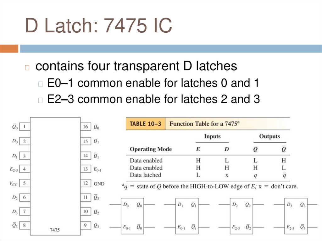
D Latch: 7475 IC◻
contains four transparent D latches
◻ E0–1 common enable for latches 0 and 1
◻ E2–3 common enable for latches 2 and 3
11.
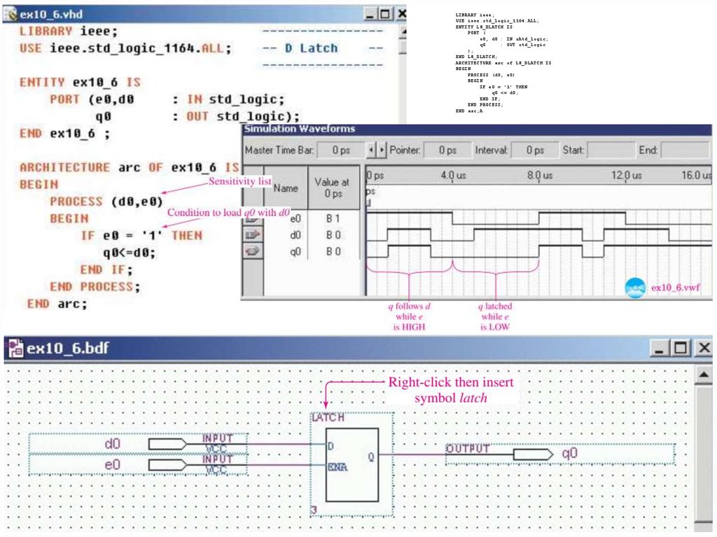
LIBRARY ieee;USE ieee.std_logic_1164.ALL;
ENTITY L8_DLATCH IS
PORT (
e0, d0 : IN sAtd_logic;
q0
: OUT std_logic
);
END L8_DLATCH;
ARCHITECTURE arc of L8_DLATCH IS
BEGIN
PROCESS (d0, e0)
BEGIN
IF e0 = '1' THEN
q0 <= d0;
END IF;
END PROCESS;
END arc;A
12.
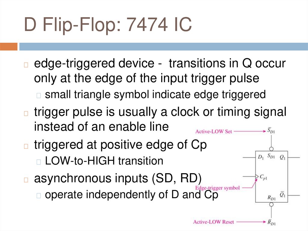
D Flip-Flop: 7474 IC◻
edge-triggered device - transitions in Q occur
only at the edge of the input trigger pulse
◻ small triangle symbol indicate edge triggered
trigger pulse is usually a clock or timing signal
instead of an enable line
◻ triggered at positive edge of Cp
◻
◻ LOW-to-HIGH transition
◻
asynchronous inputs (SD, RD)
◻ operate independently of D and Cp
13.
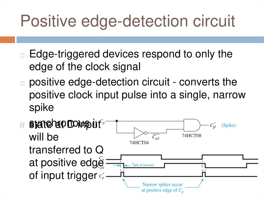
Positive edge-detection circuitEdge-triggered devices respond to only the
edge of the clock signal
◻ positive edge-detection circuit - converts the
positive clock input pulse into a single, narrow
spike
◻ state
synchronous
inputs - D (Data) and Cp (Clock)
◻
at D input
will be
transferred to Q
at positive edge
of input trigger
◻
14.
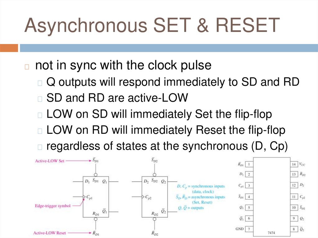
Asynchronous SET & RESET◻
not in sync with the clock pulse
◻ Q outputs will respond immediately to SD and RD
◻ SD and RD are active-LOW
◻ LOW on SD will immediately Set the flip-flop
◻ LOW on RD will immediately Reset the flip-flop
◻ regardless of states at the synchronous (D, Cp)
inputs
15.
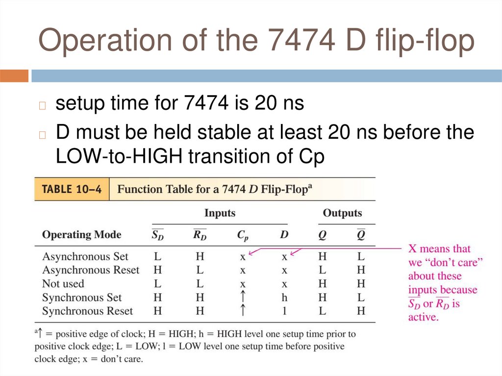
Operation of the 7474 D flip-flopsetup time for 7474 is 20 ns
◻ D must be held stable at least 20 ns before the
LOW-to-HIGH transition of Cp
◻
16.
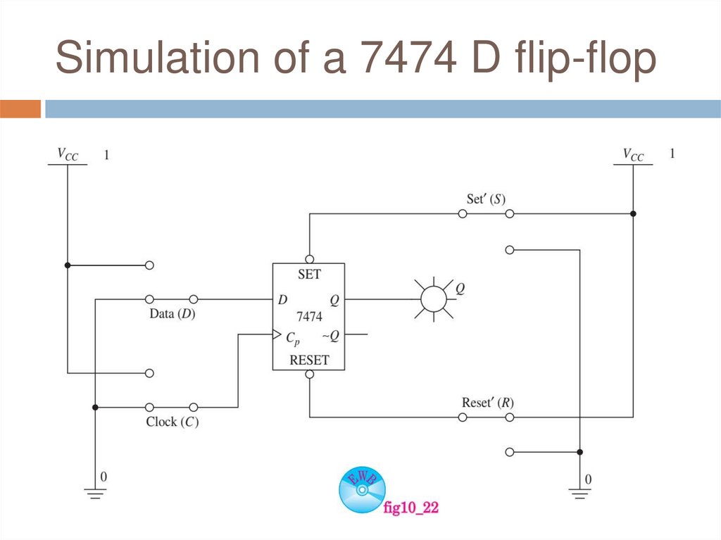
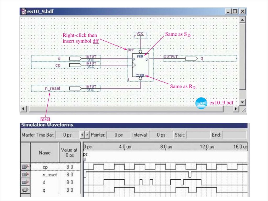
Simulation of a 7474 D flip-flop17.
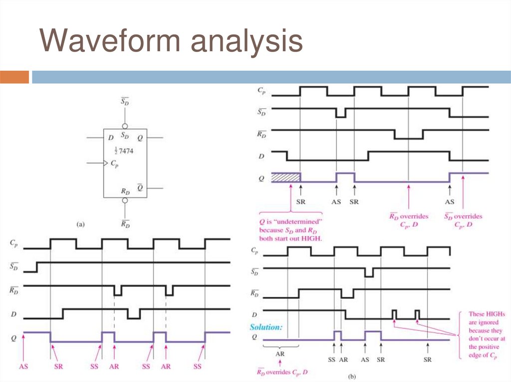
Waveform analysis18.
Review Questions1.
2.
3.
4.
The 7475 IC contains how many D latches?
The Q output of the 7475 D latch follows the
level on the D input as long as E is
___________ (HIGH or LOW)?
The 7474 is an edge-triggered device. What
does this mean?
Which are the synchronous and which are
the asynchronous inputs to the 7474 D flipflop?
19.
20.
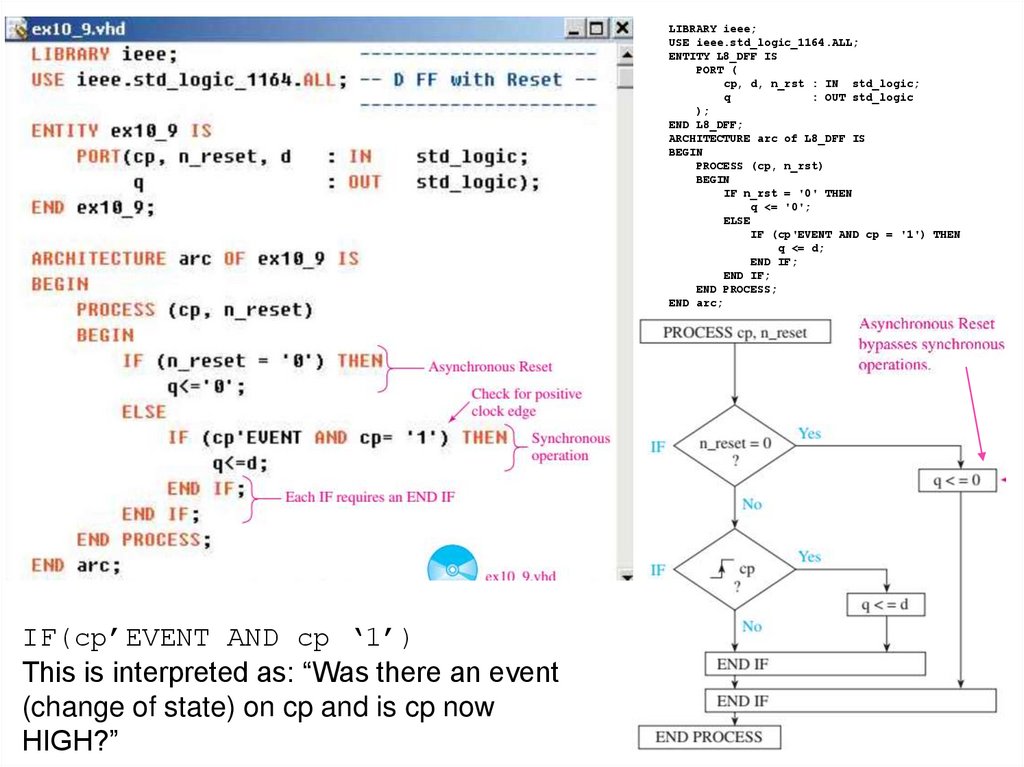
LIBRARY ieee;USE ieee.std_logic_1164.ALL;
ENTITY L8_DFF IS
PORT (
cp, d, n_rst : IN std_logic;
q
: OUT std_logic
);
END L8_DFF;
ARCHITECTURE arc of L8_DFF IS
BEGIN
PROCESS (cp, n_rst)
BEGIN
IF n_rst = '0' THEN
q <= '0';
ELSE
IF (cp'EVENT AND cp = '1') THEN
q <= d;
END IF;
END IF;
END PROCESS;
END arc;
IF(cp’EVENT AND cp ‘1’)
This is interpreted as: “Was there an event
(change of state) on cp and is cp now
HIGH?”
21.
LIBRARY ieee;USE ieee.std_logic_1164.ALL;
ENTITY L8_DFF IS
PORT (
cp, d, n_rst, n_set : IN std_logic;
q
: OUT std_logic
);
END L8_DFF;
ARCHITECTURE arc of L8_DFF IS
BEGIN
PROCESS (cp, n_rst, n_set)
BEGIN
IF (n_rst = '0' AND n_set = '1') THEN
q <= '0';
ELSIF (n_rst = '1' AND n_set = '0') THEN
q <= '1';
ELSIF (cp'EVENT AND cp = '1') THEN
q <= d;
END IF;
END PROCESS;
END arc;
22.
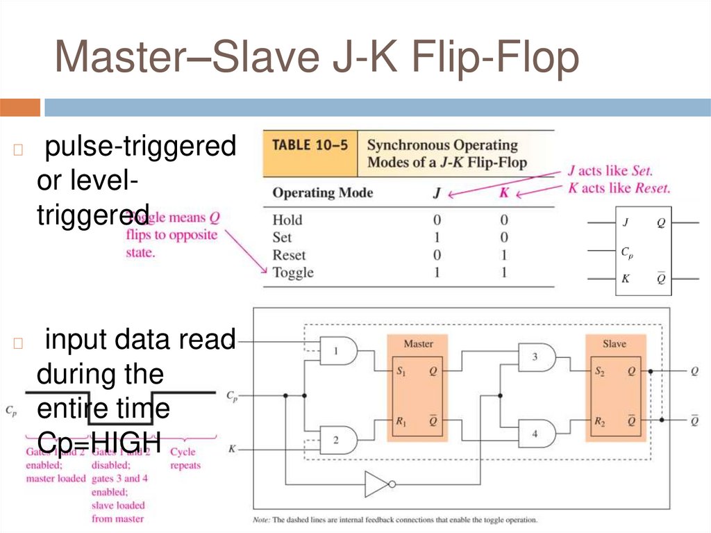
Master–Slave J-K Flip-Flop◻
pulse-triggered
or leveltriggered
◻
input data read
during the
entire time
Cp=HIGH
23.
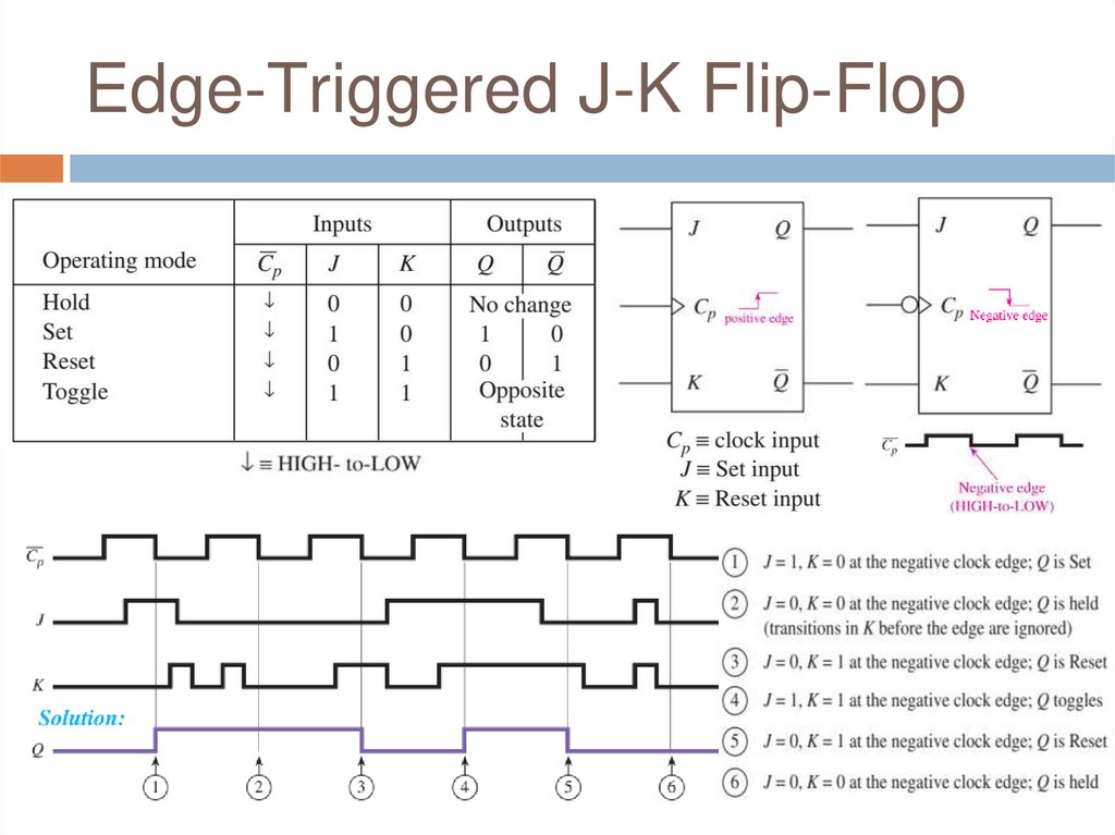
Edge-Triggered J-K Flip-Flop24.
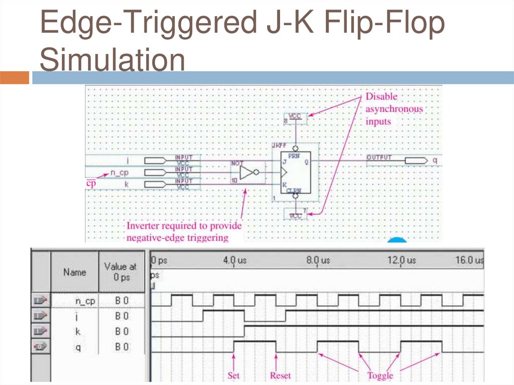
Edge-Triggered J-K Flip-FlopSimulation
25.
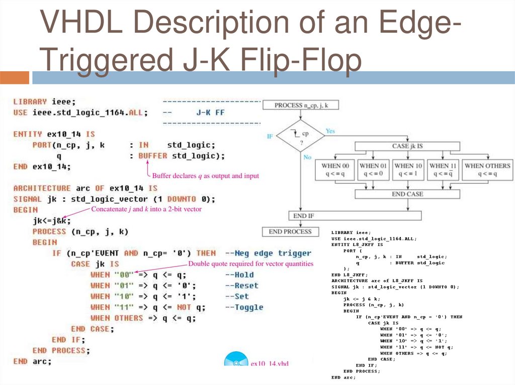
VHDL Description of an EdgeTriggered J-K Flip-FlopLIBRARY ieee;
USE ieee.std_logic_1164.ALL;
ENTITY L8_JKFF IS
PORT (
n_cp, j, k : IN
std_logic;
q
: BUFFER std_logic
);
END L8_JKFF;
ARCHITECTURE arc of L8_JKFF IS
SIGNAL jk : std_logic_vector (1 DOWNTO 0);
BEGIN
jk <= j & k;
PROCESS (n_cp, j, k)
BEGIN
IF (n_cp'EVENT AND n_cp = '0') THEN
CASE jk IS
WHEN "00" => q <= q;
WHEN "01" => q <= '0';
WHEN "10" => q <= '1';
WHEN "11" => q <= NOT q;
WHEN OTHERS => q <= q;
END CASE;
END IF;
END PROCESS;
END arc;
26.
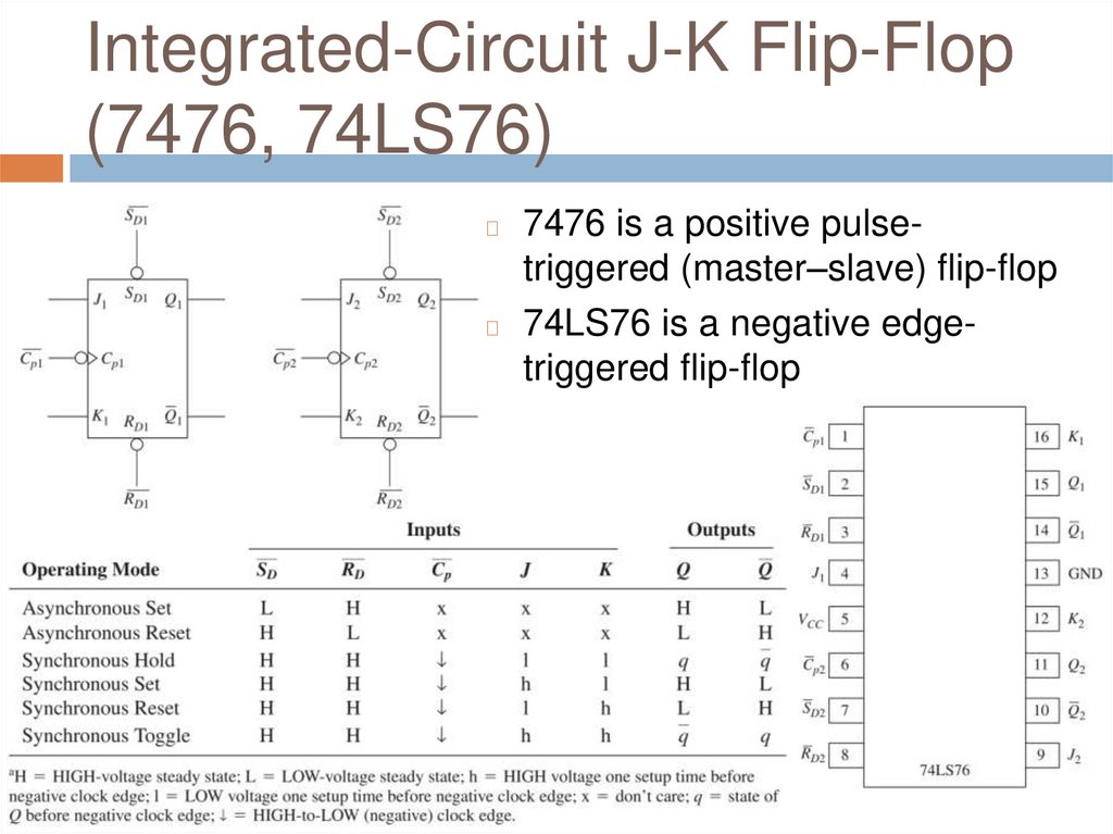
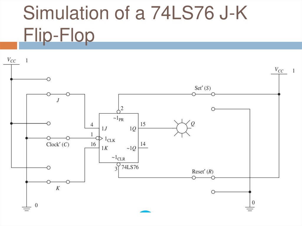
Integrated-Circuit J-K Flip-Flop(7476, 74LS76)
7476 is a positive pulsetriggered (master–slave) flip-flop
◻ 74LS76 is a negative edgetriggered flip-flop
◻
27.
Simulation of a 74LS76 J-KFlip-Flop
28.
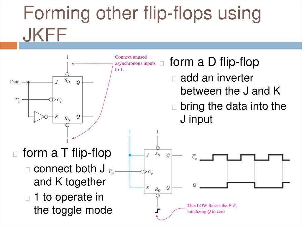
Forming other flip-flops usingJKFF
◻
form a D flip-flop
◻ add an inverter
between the J and K
◻ bring the data into the
J input
◻
form a T flip-flop
◻ connect both J
and K together
◻ 1 to operate in
the toggle mode
29.
Review Questions1.
2.
3.
4.
The Set input to a J-K flip-flop is _________
(J, K) and the Reset input is ___________ (J,
K).
The edge-triggered J-K flip-flop looks only at
the J-K inputs that are present during the
active clock edge on Cp. True or false?
What effect does the toggle operation of a JK flip-flop have on the Q output?
The synchronous inputs to the 74LS76
override the asynchronous inputs. True or
false?
30.
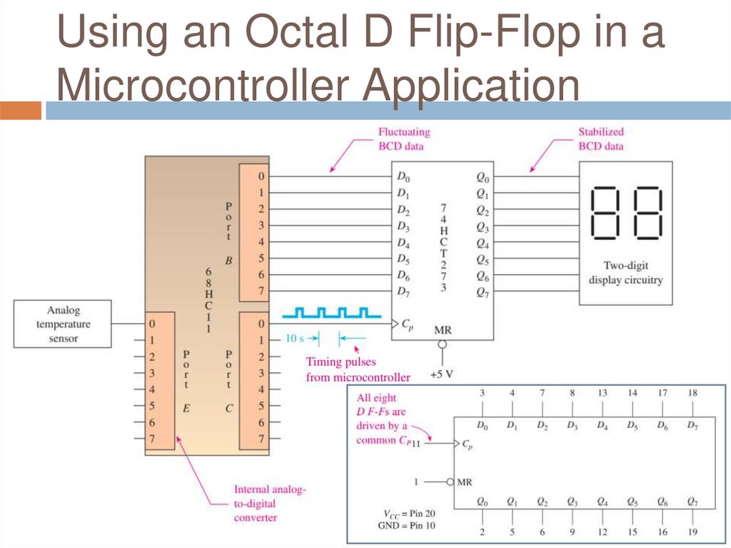
Using an Octal D Flip-Flop in aMicrocontroller Application
31.
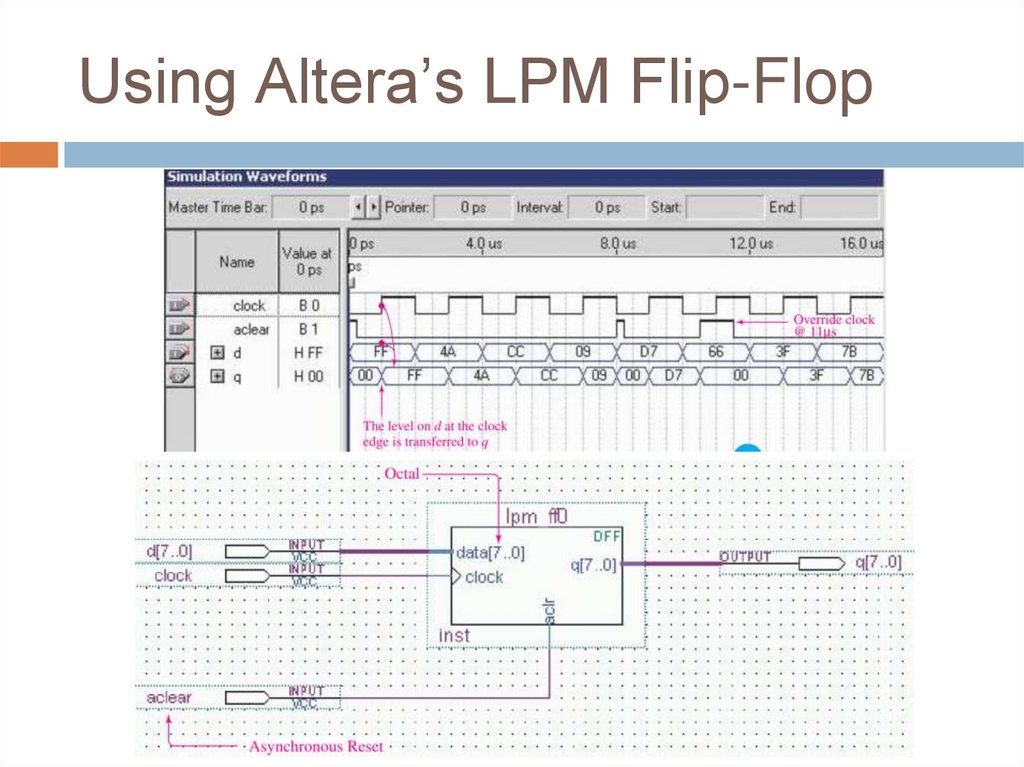
Using Altera’s LPM Flip-Flop32.
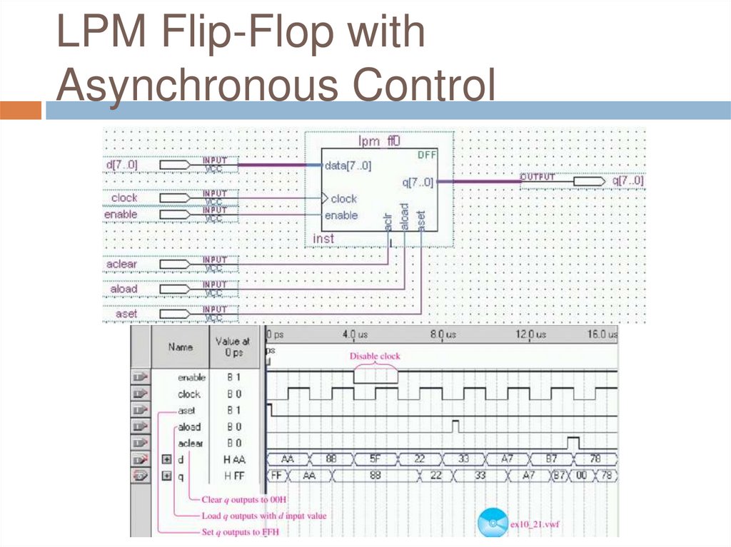
LPM Flip-Flop withAsynchronous Control
33.
Q&AAny Questions?