


 Электроника
Похожие презентации:

")


Instrumentation Amplifier Noise Analysis
1. Instrumentation Amplifier Noise Analysis
12.
23. Three Stage IA
Gain SetResistor
Vin-
5V
Rg 1k
Vin- = 2.499V
+
-
150k
150k
A1
-
50k
A3
+
50k
Output
Voltage
Vin_dif = 2mV
+
Vin+
Differential
Input Voltage
Vout
Vin+ = 2.501V
150k
150k
A2
Reference
Input
3
4. Real World Input to Mathematical Model
VccVdif
Vinp + Vinn
Vcm =
2
+
Vinn
-Vdif
2
+
+
Vinp
Vdif
2
4
5. Analyze the Input and Output Separately
VssVEE1 12
Vcc
VCC1 12
-Vdif
2
Vin-
Vcc
Va1
+
+
-
R3 40k
R5 40k
A1
Vss
R1 25k
R7 49.9
Vss
VCM
+
-
A3
Vout
+
R2 25k
Vcc
Vss
-
Vdif
2
R4 40k
+
+
A2
R6 40k
Va2
Vcc
Vin+
Input Stage
Differential Gain Stage
Output Stage
Dif Amp
5
6. Split Input Stage in Half
-Vdif2
Va1
Vin-
+
-Vdif
2
VCM Vin-
+
+
- A1
Rg 1k
A1
Split Input Stage
50k
Rg
2
+
VCM
+
Vdif
2
Va1
Rf
Rg
2
+
+
+
-
VCM
50k
VCM
R
Vdif
1+2 f
Rg
2
+
Vin+
Rf
-
A2
Va2
Input Stage
Differential Gain Stage
Vdif
2
+ Vin+
VCM +
+
A2
Va2
R
Vdif
1+2 f
Rg
2
6
7. Use Superposition on Output Amp
Va1Va1
R3 40k
R3 40k
R5 40k
Va1
R5 40k
Va1
Inverting Amp
Gain = -1
-
Vin_dif
Va2
A3
R3 40k
R6 40k
Va2
Output Stage
Dif Amp
Vout
+
-Va1
Vout
+
R4 40k
A3
-
Non-inverting Amp
Gain = 2
Voltage Divider
Gain = 1/2
Va2
Va2
R5 40k
+
R4 40k
Va2
Vref
+
2
2
A3
Vout
Va2 + Vref
R6 40k
Vref
Find Vout Through Superposition
Vout = Va2 – Va1 + Vref
7
8. Gain For Three Amp IA
RfVa1 Vcm
1 2
2
Rg
[1] Input Stage
Top Half
Rf
Va2 Vcm
1 2
2
Rg
[2] Input Stage
Bottom Half
Vdif
Vdif
Vout
Va2 Va1 Vref
Vout
Vdif
Rf
Vdif
Rf
Vcm 2 1 2 R Vcm 2 1 2 R Vref
g
g
Vout
Rf
Vdif 1 2
Vref
Rg
[3] Output Stage
Substitute
[1] and [2]
into [3]
[4] Simplify
8
9.
910. Complex Noise Model
-Vdif2
Vin-
Vcc
Va1
+
+
-
R5 40k
A1
Vss
R1 25k
R7 49.9
Vss
VCM
+
-
A3
Vout
+
R2 25k
Vcc
Vss
-
Vdif
2
+
R6 40k
+
A2
Va2
Vcc
Vin+
10
11. The Complex Model is Simplified
Input Stagein_out
Input
gain = G
Output Stage
Vn_out
Output
gain = 1
Vout
Vn_in
in_out
Vn_RTI
Total
gain = G
Vn_out
Vn_RTI
Vn_out
2
Vn_in G
2
Vout
Vn_out
G
2
2
Vn_in
11
12. The Input amplifier dominates at High Gain
From INA333 Data SheetG
Total InputReferred
Noise
(nV/rtHz)
Total Output
Noise
(nV/rtHz)
1
206.2
206.2
2
111.8
223.6
5
64
320
10
53.9
539
100
50
5000
1000
50
50,000
12
13.
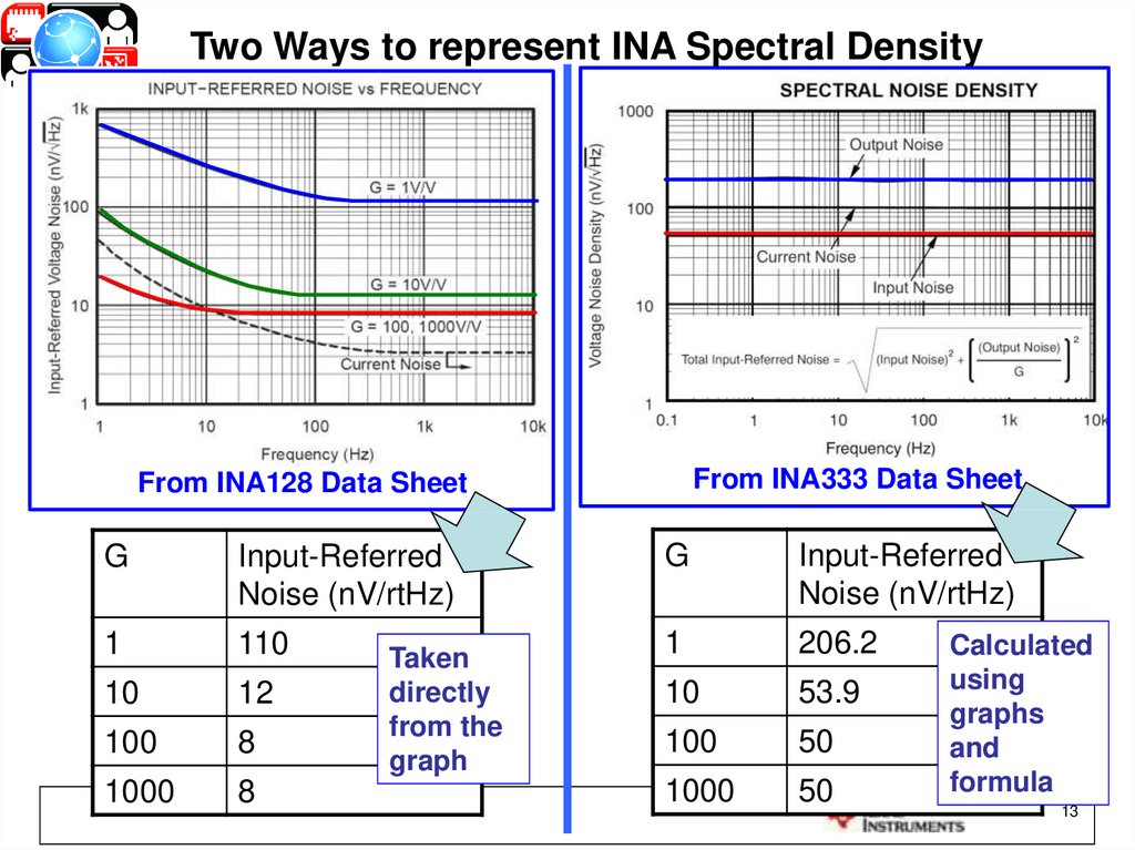
Two Ways to represent INA Spectral DensityFrom INA333 Data Sheet
From INA128 Data Sheet
G
Input-Referred
Noise (nV/rtHz)
G
Input-Referred
Noise (nV/rtHz)
1
110
1
206.2
10
12
10
53.9
100
8
100
50
1000
8
1000
50
Taken
directly
from the
graph
Calculated
using
graphs
and
formula
13
14.
1415. Find the total RMS Noise Voltage at the Output
+V= 5V5V
Vin- = 2.499V
+
A1
-
150k
150k
Rg 1k
5k
5k
Vss
50k
INA333
Vout
A3
+
5k
5k
50k
-
Vin_dif = 2mV
-
150k
150k
A2
+
Vss
Vin+ = 2.501V
5V
-V= GND
100k
+
100k
15
16. Look at Noise Sources: Bridge, INA333, Reference Buffer
+V= 5V5V
Vin- = 2.499V
+
A1
-
150k
150k
Rg 1k
5k
5k
Vss
50k
INA333
Vout
A3
+
5k
5k
50k
-
Vin_dif = 2mV
-
150k
150k
A2
+
Vss
Vin+ = 2.501V
5V
-V= GND
100k
+
100k
16
17. Noise Equivalent Model for Reference Pin Buffer
Vss5V
5V
100k
OPA333
+
-
Vref_pin
OPA333
100k
100fA
+
55nV
30nV
100k || 100k
50k
17
18. Reference buffer
5V-
Vref_pin
OPA333
23
kn
1.38 10
Boltzmann’s constant
Tk
273 25
Temperature in Kelvin
Req
50k
100fA
+
Input resistance
(parallel combination of voltage divider)
55nV
30nV
100k || 100k
4kn Tn Req
en_r
nV
28.7
Thermal Noise from input resistor
Hz
50k
in
Current noise from OPA333
100fA
en_i
in Req
en_opa
en_ref
55
5
nV
Voltage Noise from current noise
Hz
nV
Voltage noise from OPA333
Hz
2
2
2
en_opa en_r en_i
62.2
nV
Hz
Total rms noise from
reference driver circuit
18
19. The reference voltage directly adds to the output noise
Output StageInput Stage
in_out
Input
gain = G
Vn_in
Vn_out
Vout
Output
gain = 1
Σ
en_ref
9
en_ref 62.2 10
9
Vn_out 200 10
2
2
9
Output_Stage_Noise en_ref Vn_out 209.449 10
19
20. The bridge generates: thermal noise, in x R_bridge
en_r R/2inn
-
Vcc
R
R
+
inn
R
R
Use superposition to
combine noise sources
on the negative and
positive input.
+
inp
en_r R/2
+
inp
20
21. Noise From Bridge / Current Sources
Vcc5k
5k
R
inn
2
Voltage noise from current noise
en_rb
R
4kn Tn
2
Use superposition to add the noise from
the input resistance and both current noise sources
inn
5k
INA333
5k
2
ein_i
+
inp
Resistor Noise
2
i R e
nn n_rb
2
2
2
i R e
np n_rb
2
Assume inn
inp
Note that these sources are uncorrelated
2
ein_i
R
2
2 in 2 en_rb
2
Total Noise from input
resistors and current source
For this example (R=5kO, in = 100fA/rtHz)
nV
Resistor noise
en_rb
6.4
R
inn
2
0.25
ein_i
2 ( 0.5) 2 ( 9.1)
Hz
nV
Voltage noise from current noise
Hz
2
2
9.1
nV
Hz
Total Noise from input
21
resistors and current source
22. Combine all the noise sources
Sensor Noise9nV/rtHz
Input Stage Noise Output Stage Noise
50nV/rtHz
200nV/rtHz
+V= 5V
Vin-
5V
+
-
150k
150k
A1
Rg 1k
5k
5k
50k
INA333
5k
5k
50k
Vin+
150k
A2
-
Vout
A3
+
150k
+
Reference
Buffer Noise
62nV/rtHz
Vss
5V
-V= GND
100k
OPA333
+
100k
22
23. Rule of 3x
Vn6
1
.
3
Vn
3Vn
3 Vn
2
Vn
2
2
9 Vn Vn
2
3.16Vn
Dominant Neglect
When adding two uncorrelated noise terms, the larger term
will dominate if it is 3 times larger then the smaller term.
You can neglect the smaller term with a relatively small
error (i.e. 6%).
23
24.
For this example compute noise spectral density refered to the input2
Noise_Spec_Den_RTI
Vn_ref_buf
2
2 Vn_out_stage
Vn_in_stage Vn_bridge
G
G
Noise_Spec_Den_RTI
200
62
( 50) ( 9)
100 100
2
Dominant
2
2
Neglect
2
50.847
2
nV
Hz
Approximately equal
to the dominant term
24
25.
Bandwidthfrom Data
Sheet
For G = 100
20dB/decade
1st order
Kn = 1.57
25
26. Calculate RMS Output Noise for INA333 From Voltage Noise
G100
Vin_RTI
fH
Kn
From "Input referred noise" equation
50.85nV/rtHz
3.5kHz
From data sheet table for gain = 100
1.57
For first order function
See Gain vs Frequency in the dat a sheet
BW n
fH Kn
en_out
en_outPP
5.495kHz
G Vin_RTI BW n
6.en_out
Noise Bandwidth
376.9 Vrms
2.26mVpp
RMS Output Noise
Peak-to-Peak Output
26
27.
2728. Simulate the Circuit
VIN_N 2.5VR3 5k
RG
U1 INA333
VVout 2.5V
Out
RG
R5 5k
Ref
V+
+
VIN_P 2.5V
Vref 2.5V
Vcc
Vcc
-
Vjunk 0V
Vcc
+
+
U2 OPA333
VG1 0
V4 5
+
R6 100k
R4 5k
R1 100
-
R7 100k
R2 5k
Vcc
Vcc
28
29. Using Tina Spice
2930. Noise Spectral Density at the Output
Voltage Spectral Density Out vs. Frequency10.00u
5.2uV/rtHz
Vout
Vout (V/rtHz)
T
-3db @
3.91kHz
10.00n
1
10
100
1k
10k
100k
1M
Frequency (Hz)
30
31. Total RMS Noise at the Output
TVn output Total RMS Noise (Vrms)
500u
Simulation = 422uVrms
Hand Calc = 377uVrms
375u
250u
125u
0
1
10
100
1k
10k
100k
1M
Frequency (Hz)
31
32.
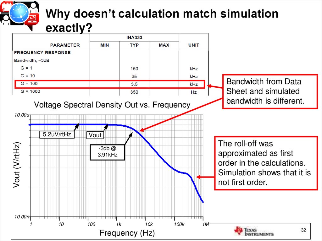
Why doesn’t calculation match simulationexactly?
Bandwidth from Data
Sheet and simulated
bandwidth is different.
Voltage Spectral Density Out vs. Frequency
10.00u
5.2uV/rtHz
Vout
Vout (V/rtHz)
T
The roll-off was
approximated as first
order in the calculations.
Simulation shows that it is
not first order.
-3db @
3.91kHz
10.00n
1
10
100
1k
10k
Frequency (Hz)
100k
1M
32
33.
3334. Averaging Circuit
RfR1
V1
Vcc
-
Vout
R2
+
V2
OPA335
Vss
R3
Vref
V3
RN
VN
Vout
V1 V2 V3
Vref Rf
...
R1 R2 R3
VN
RN
[15]
For an averaging circuit choose
R1 = R 2 = R 3 = ... R N = R
Rf = R / N
Vout
Vref
V1 V2 V3 ... VN
[16]
N
34
35. Noise in Averaging Circuit
v noise_outputvnoise1
N
2
vnoise2
N
2
vnoise3
N
2
vnoiseN
...
N
2
Where v noise1 , vnoise2 , vnoise3 , ... vnoiseN are noise sources
If you assume that v noise1 , vnoise2 , vnoise3 , ... vnoiseN are equal
uncorrelated noise sources, then
v noise_output
vnoise
N
N
2
v noise
N
2
v noise
N
[17]
35
36. Averaging Circuit with INA333
Vss+
Vdif
2.4mV
R1 100
2
1
4
U1
RG V-
R4 100k
INA333
8
Out
Ref
6
RG V+
3
72uA
24uA
5
+
R7 33.3k
7
V2 2.5
Vcc
Vref
Vss
Vss
R2 100
2
1
_
-
4
U2
RG V-
8
Vout
+
U4
OPA335
Out
Ref
6
RG V+
Vcc
24uA
Vref
5
+
+
R5 100k
INA333
3
7
2.4V
Vref
Vcc Vref
Vss
2
R3 100
2.5V
_
1
_
4
U2
RG V-
R6 100k
INA333
8
Out
Ref
RG V+
3
6
24uA
5
+
2.4V
7
Vcc
Vref
36
Vref
37. Experiment with 20 Parallel INA333
Socketed GainSet Resistors
20 INA333 amps in parallel
(jumper selectable)
OPA333
Averaging
Circuit
37
38. Standard Noise Measurement Precautions
Linear PowerSource
Steel Paint Can
for Shielding
38
39. Total Output Noise vs Number of Amplifiers Being Averaged
Noise vs Number of Amplifiers0.0016
Total Output Noise (V rms)
0.0014
measured
0.0012
ideal (from tina)
0.001
0.0008
0.0006
0.0004
0.0002
0
0
5
10
15
20
Number of Amplifiers in Average Circuit
39
40.
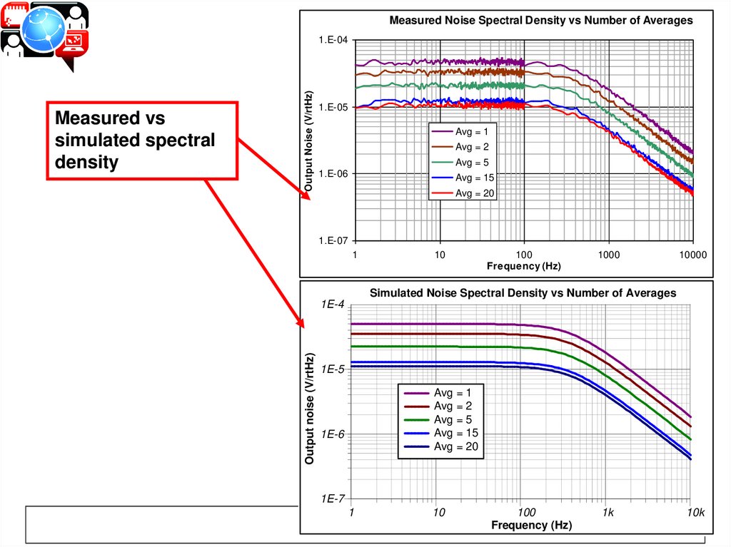
Measured Noise Spectral Density vs Number of Averages1.E-05
Avg = 1
Avg = 2
Avg = 5
1.E-06
Avg = 15
Avg = 20
1.E-07
1
10
100
Frequency (Hz)
1000
10000
Simulated Noise Spectral Density vs Number of Averages
1E-4
Output noise (V/rtHz)
Measured vs
simulated spectral
density
Output Noise (V/rtHz)
1.E-04
1E-5
Avg = 1
Avg = 2
Avg = 5
Avg = 15
Avg = 20
1E-6
1E-7
1
10
100
Frequency (Hz)
1k
10k
40
41.
References1.
2.
[1] Hann, Gina. "Selecting the right op amp - Electronic Products." Electronic Products Magazine – Component and Technology
News. 21 Nov. 2008. Web. 09 Dec. 2009. <http://www2.electronicproducts.com/Selecting_the_right_op_amp-articlefacntexas_nov2008-html.aspx>.
Henry W. Ott, Noise Reduction Techniques in Electronics Systems, John Wiley and Sons
Acknowledgments:
1.
2.
3.
8.
R. Burt, Technique for Computing Noise based on Data Sheet Curves, General Noise Information
T. Green, General Information
B. Trump, General Information
Matt Hann, General INA information and review
Noise Article Series (www.en-genius.net)
http://www.en-genius.net/site/zones/audiovideoZONE/technical_notes/avt_022508
41
42.
Thank Youfor
Your Interest
in
INA Noise – Calculation and Measurement
42