Похожие презентации:
Interconnect delay. (Chapter 7)
1. EE 201A (Starting 2005, called EE 201B) Modeling and Optimization for VLSI Layout
Instructor:Lei He
Email:
LHE@ee.ucla.edu
2. Chapter 7 Interconnect Delay
7.1 Elmore Delay7.2 High-order model and moment matching
7.3 Stage delay calculation
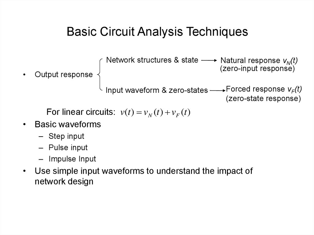
3. Basic Circuit Analysis Techniques
Network structures & stateOutput response
Input waveform & zero-states
Natural response vN(t)
(zero-input response)
Forced response vF(t)
(zero-state response)
For linear circuits: v(t ) vN (t ) vF (t )
• Basic waveforms
– Step input
– Pulse input
– Impulse Input
• Use simple input waveforms to understand the impact of
network design
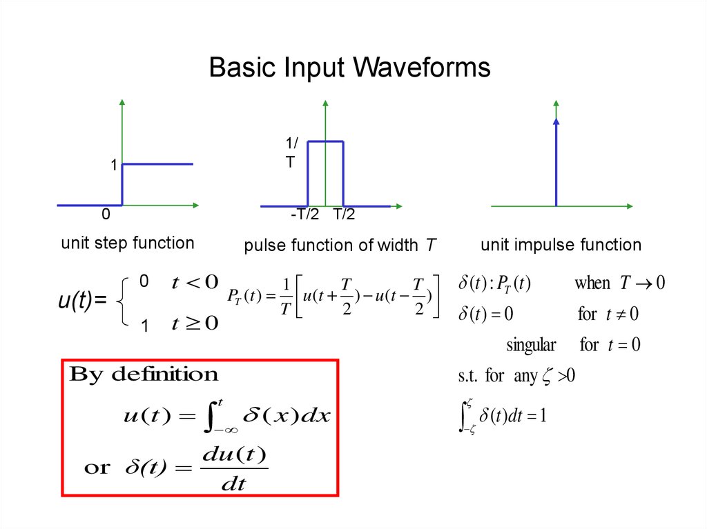
4. Basic Input Waveforms
1/T
1
0
-T/2 T/2
unit step function
u(t)=
0
t 0
1
t 0
PT (t )
1
T
T
T
u
(
t
)
u
(
t
)
2
2
By definition
u (t )
or δ(t)
unit impulse function
pulse function of width T
t
( x ) dx
du (t )
dt
(t ) : PT (t )
when T 0
(t ) 0
for t 0
singular for t 0
s.t. for any 0
(t )dt 1
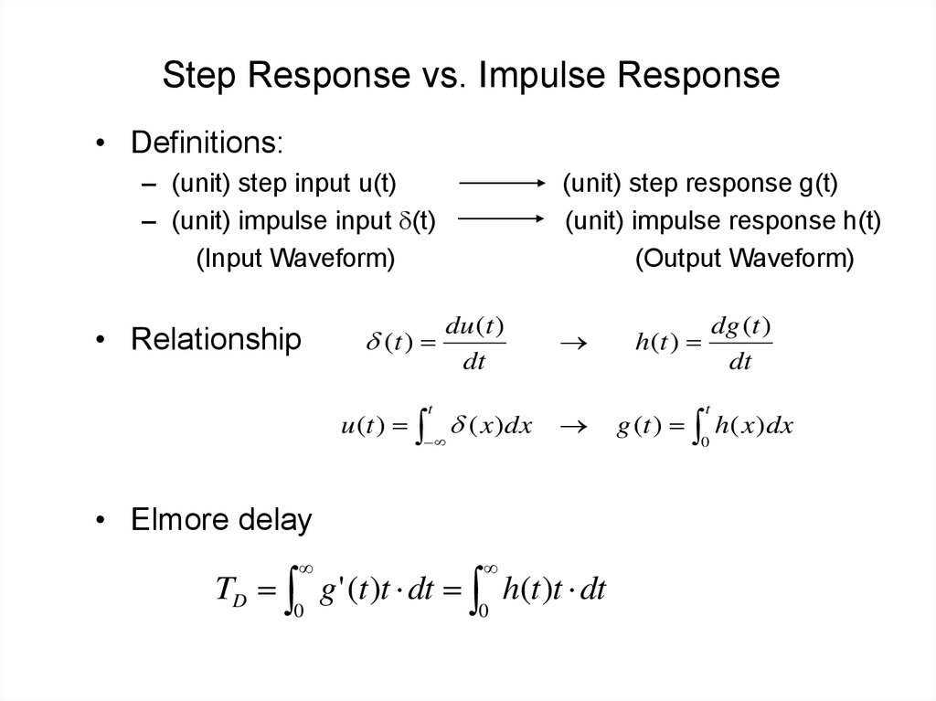
5. Step Response vs. Impulse Response
• Definitions:– (unit) step input u(t)
– (unit) impulse input (t)
(Input Waveform)
• Relationship
(t )
(unit) step response g(t)
(unit) impulse response h(t)
(Output Waveform)
du (t )
dt
t
u (t ) ( x ) dx
• Elmore delay
0
0
TD g ' (t )t dt h(t )t dt
dg (t )
dt
h(t )
t
g (t ) h( x ) dx
0
6. Analysis of Simple RC Circuit
R i (t ) v (t ) vT (t )d (Cv(t ))
dv (t )
i (t )
C
dt
dt
dv(t )
RC
v (t ) vT (t )
dt
state
variable
Input
waveform
i(t)
R
vT(t)
±
C
v(t)
first-order linear differential
equation with
constant coefficients
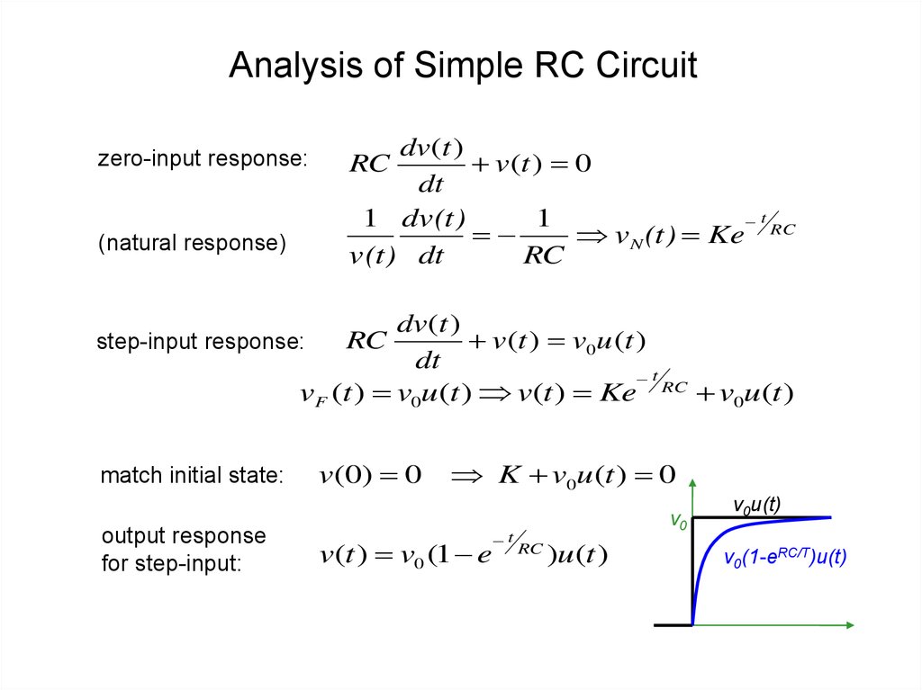
7. Analysis of Simple RC Circuit
zero-input response:(natural response)
dv(t )
v(t ) 0
dt
1 dv(t)
1
t
v N (t) Ke RC
v(t) dt
RC
RC
dv(t )
RC
v(t ) v0u (t )
step-input response:
dt
t
vF (t ) v0u(t ) v(t ) Ke RC v0u(t )
match initial state:
output response
for step-input:
v(0) 0
K v0u (t ) 0
v(t ) v0 (1 e
t
v0
RC
)u (t )
v0u(t)
v0(1-eRC/T)u(t)
8. Delays of Simple RC Circuit
• v(t) = v0(1 - e-t/RC) under step input v0u(t)• v(t)=0.9v0 t = 2.3RC
v(t)=0.5v0 t = 0.7RC
• Commonly used metric
TD = RC (Elmore delay to be defined later)
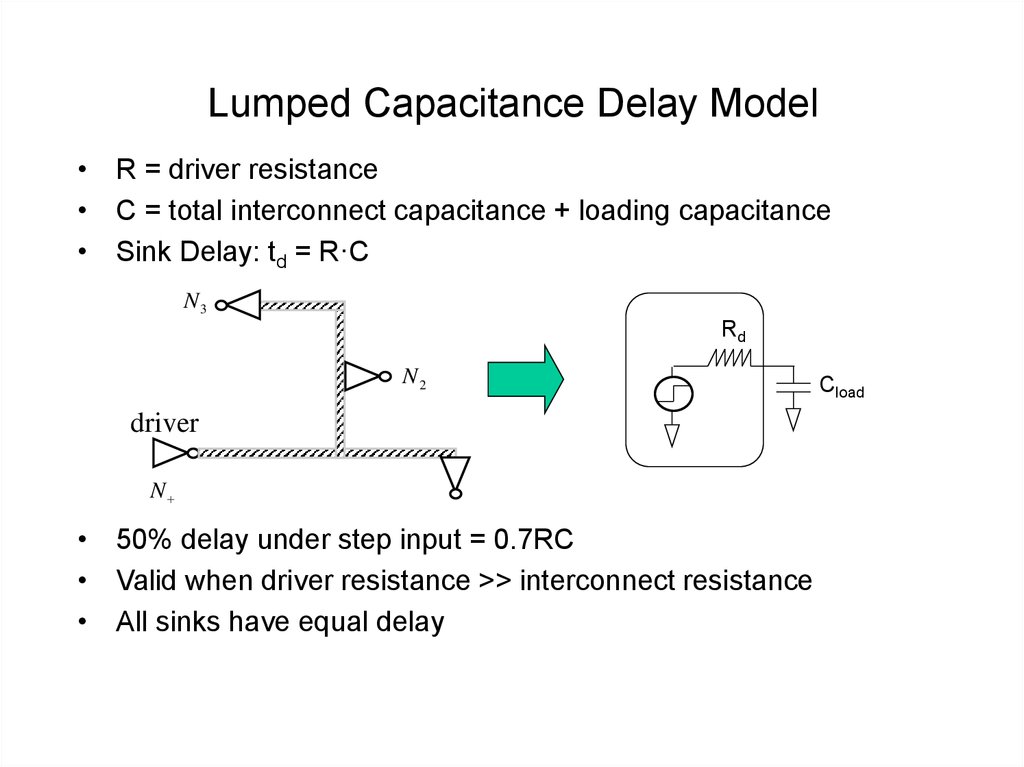
9. Lumped Capacitance Delay Model
• R = driver resistance• C = total interconnect capacitance + loading capacitance
• Sink Delay: td = R·C
N3
Rd
N2
driver
N
• 50% delay under step input = 0.7RC
• Valid when driver resistance >> interconnect resistance
• All sinks have equal delay
Cload
10. Lumped RC Delay Model
t D R d Cload R d Cint CgR d C0 L Cg
• Minimize delay minimize wire length
N3
Rd
N2
driver
N
Cload
11. Delay of Distributed RC Lines
Vout(t)Laplace
Transform
Vout(s)
VIN
R
VOUT
VIN
R
VOUT
C
C
VOUT
1
s cosh sRC
e x e x
cosh( x)
2
x2 x4
1 ......
2! 4!
Vout ( s )
1.0
0.5
DISTRIBUTED
LUMPED
1.0RC
2.0RC
time
Step response of distributed and lumped RC networks.
A potential step is applied at VIN, and the resulting VOUT
is plotted. The time delays between commonly used
reference points in the output potential is also tabulated.
12. Delay of Distributed RC Lines (cont’d)
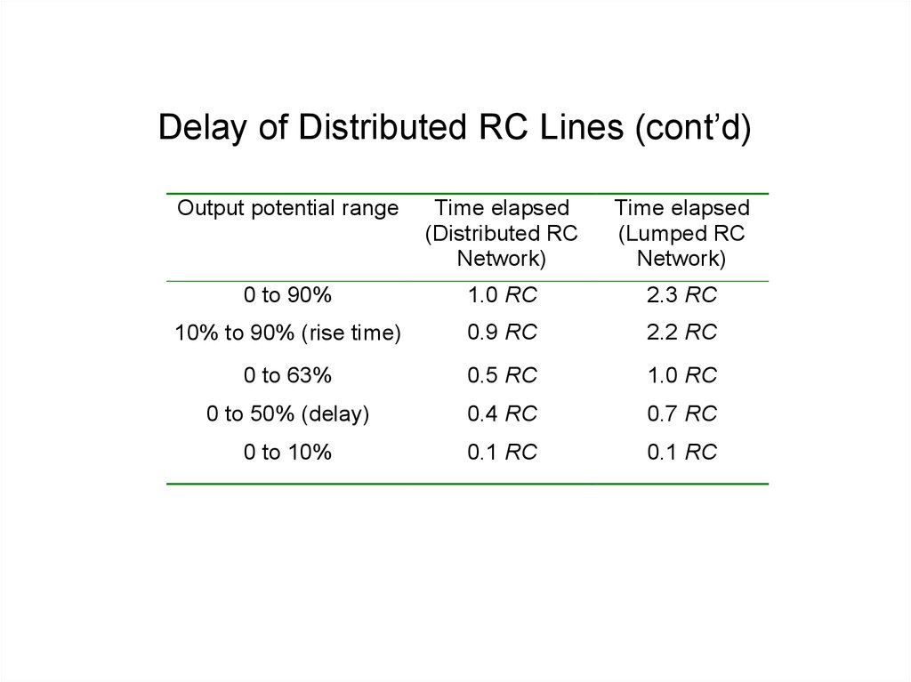
Output potential rangeTime elapsed
(Distributed RC
Network)
Time elapsed
(Lumped RC
Network)
0 to 90%
1.0 RC
2.3 RC
10% to 90% (rise time)
0.9 RC
2.2 RC
0 to 63%
0.5 RC
1.0 RC
0 to 50% (delay)
0.4 RC
0.7 RC
0 to 10%
0.1 RC
0.1 RC
13. Distributed Interconnect Models
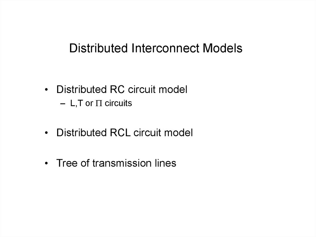
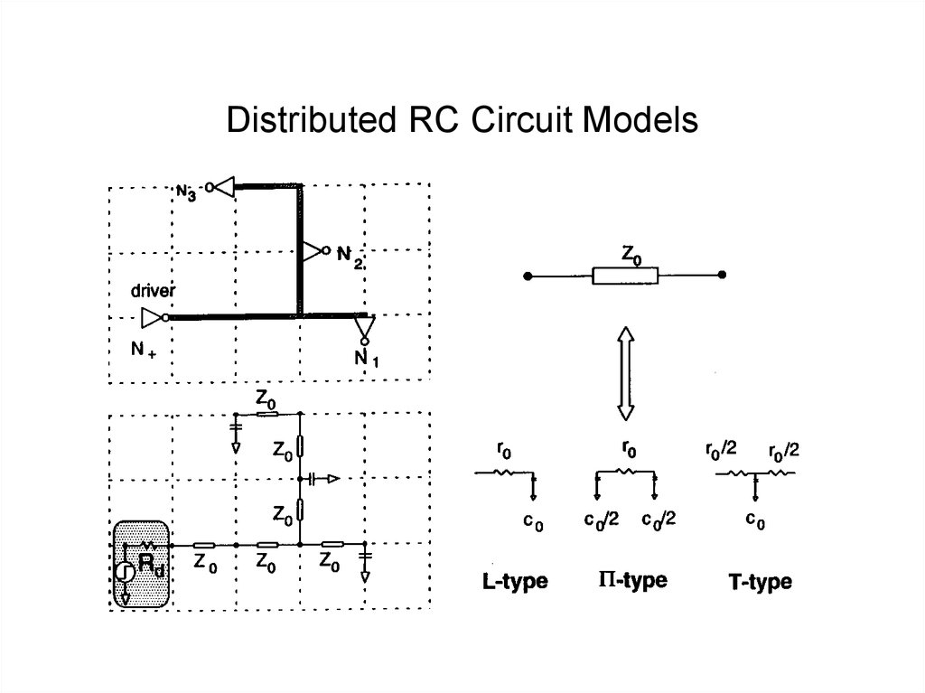
• Distributed RC circuit model– L,T or P circuits
• Distributed RCL circuit model
• Tree of transmission lines
14. Distributed RC Circuit Models
15. Distributed RLC Circuit Model (without mutual inductance)
Z0Z0
16. Delays of Complex Circuits under Unit Step Input
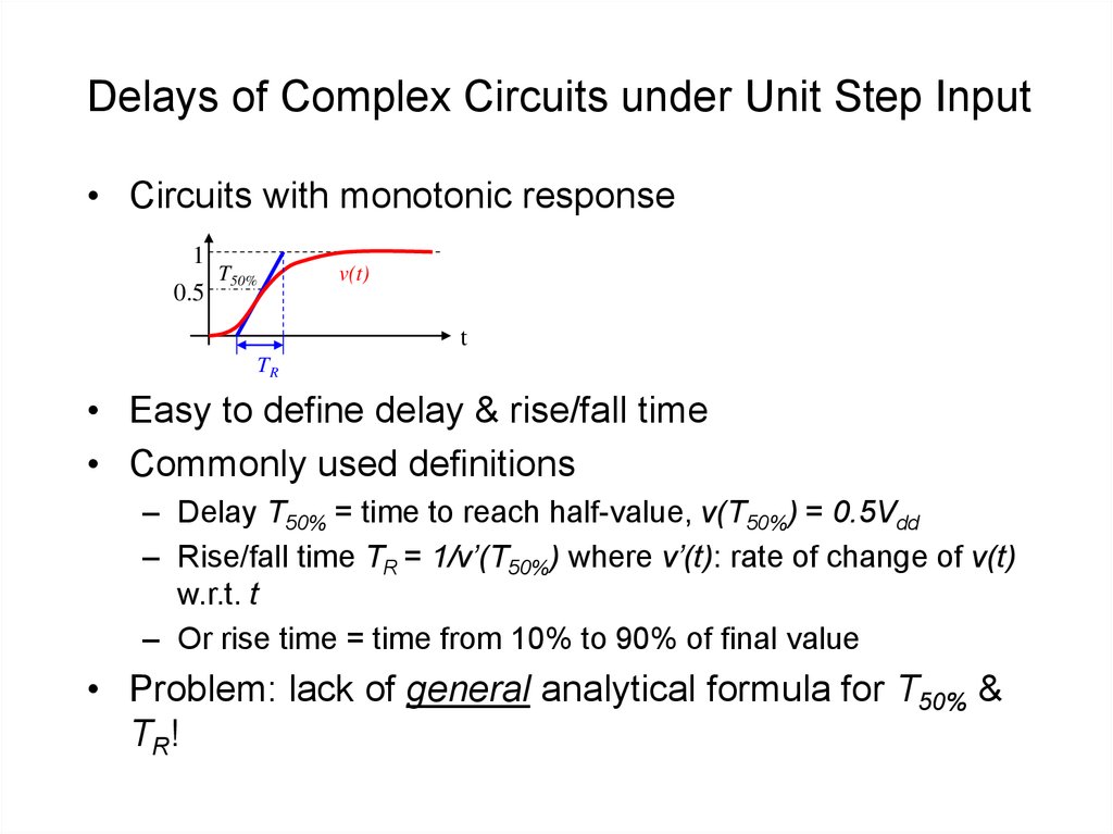
• Circuits with monotonic response1
0.5
T50%
v(t)
t
TR
• Easy to define delay & rise/fall time
• Commonly used definitions
– Delay T50% = time to reach half-value, v(T50%) = 0.5Vdd
– Rise/fall time TR = 1/v’(T50%) where v’(t): rate of change of v(t)
w.r.t. t
– Or rise time = time from 10% to 90% of final value
• Problem: lack of general analytical formula for T50% &
TR!
17. Delays of Complex Circuits under Unit Step Input (cont’d)
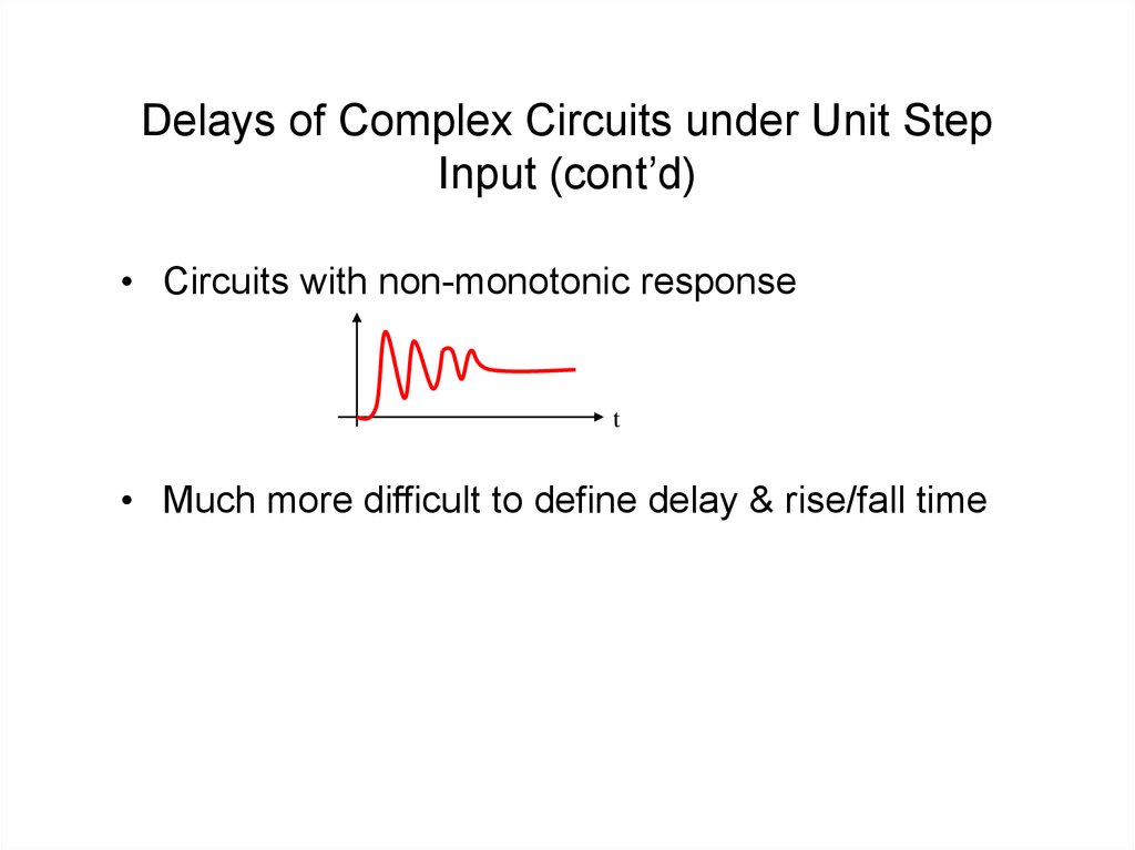
• Circuits with non-monotonic responset
• Much more difficult to define delay & rise/fall time
18. Elmore Delay for Monotonic Responses
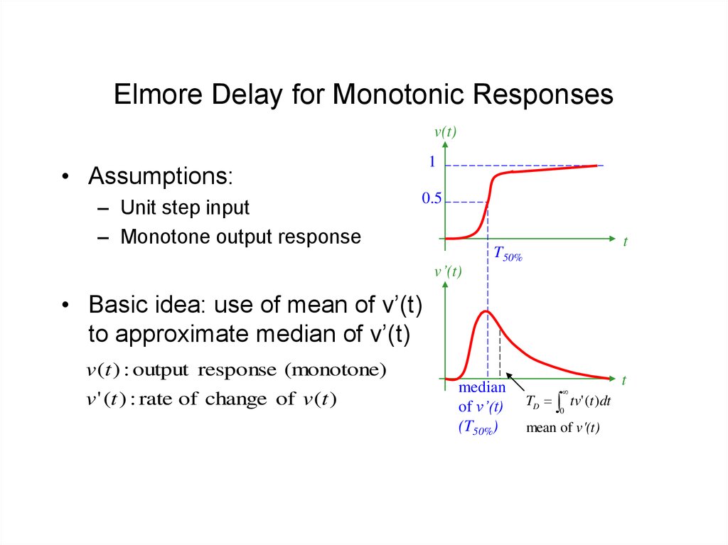
v(t)1
• Assumptions:
– Unit step input
– Monotone output response
0.5
t
T50%
v’(t)
• Basic idea: use of mean of v’(t)
to approximate median of v’(t)
v(t ) : output response (monotone)
v' (t ) : rate of change of v(t )
median
of v’(t)
(T50%)
TD tv' (t )dt
0
mean of v'(t)
t
19. Elmore Delay for Monotonic Responses
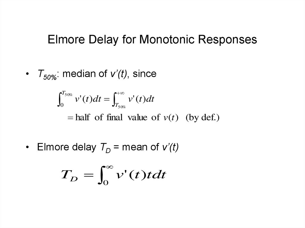
• T50%: median of v’(t), sinceT5 0%
0
v' (t )dt
T5 0%
v' (t )dt
half of final value of v(t ) (by def.)
• Elmore delay TD = mean of v’(t)
TD
0
v' (t )tdt
20. Why Elmore Delay?
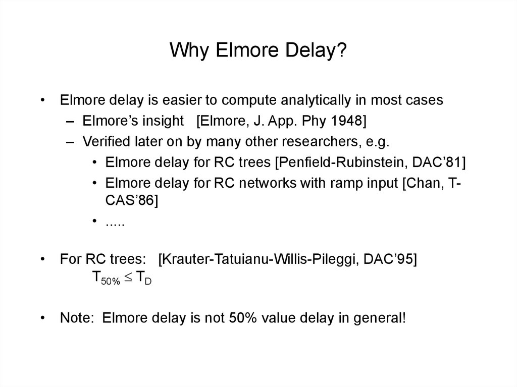
• Elmore delay is easier to compute analytically in most cases– Elmore’s insight [Elmore, J. App. Phy 1948]
– Verified later on by many other researchers, e.g.
• Elmore delay for RC trees [Penfield-Rubinstein, DAC’81]
• Elmore delay for RC networks with ramp input [Chan, TCAS’86]
• .....
• For RC trees: [Krauter-Tatuianu-Willis-Pileggi, DAC’95]
T50% TD
• Note: Elmore delay is not 50% value delay in general!
21. Elmore Delay for RC Trees
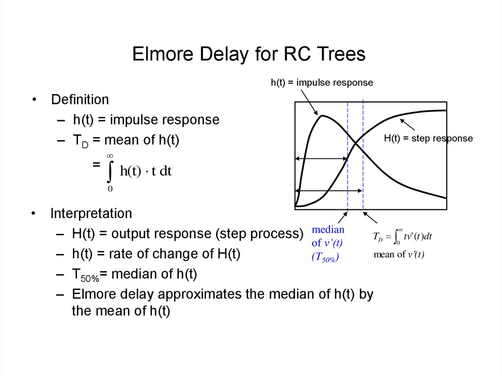
h(t) = impulse response• Definition
– h(t) = impulse response
– TD = mean of h(t)
=
H(t) = step response
h(t) t dt
0
• Interpretation
– H(t) = output response (step process) median
TD tv' (t )dt
0
of v’(t)
mean of v'(t)
– h(t) = rate of change of H(t)
(T50%)
– T50%= median of h(t)
– Elmore delay approximates the median of h(t) by
the mean of h(t)
22. Elmore Delay of a RC Tree [Rubinstein-Penfield-Horowitz, T-CAD’83]
Lemma: when a step input is applied to a RC treevi (t ) is monotonic in t for every node i in tree
Proof:
v'i (t ) 0 at every node i (v' i (t ) hi (t ))
impulse response hi (t ) 0 at every node i
Apply impulse func. at t=0:
Let hmin (t ) be the min. voltage of any node at t
hmin (0 ) 0
Assume that hmin (t0 ) 0
Then, t1 t0
imin
s.t. h'min (t1 ) 0
Let node imin achieve hmin (t1 ) at t1
Then, the current from any node i to imin is 0 at t1
Since hi (t1 ) hmin (t1 ) & i connects imin via resistors
current i imin
i
Since all currents i imin charge the capacitor at imin
h'min (t1 ) 0 contradict ion!
23. Elmore Delay in a RC Tree (cont’d)
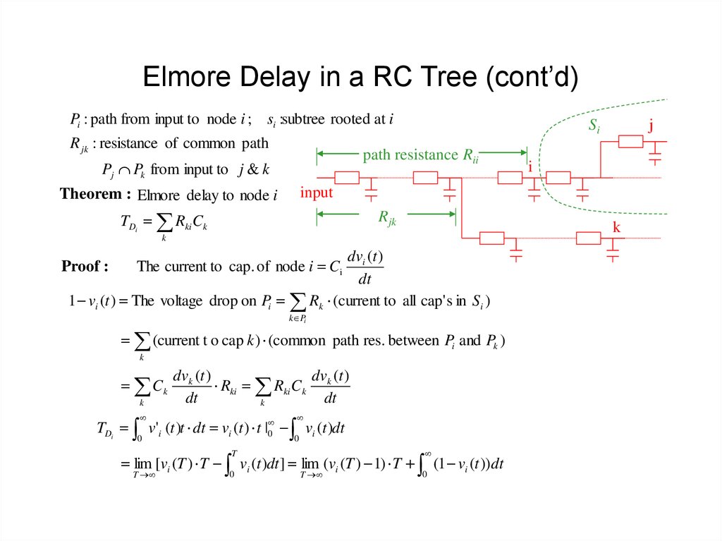
Pi : path from input to node i ; si :subtree rooted at iR jk : resistance of common path
Si
path resistance Rii
Pj Pk from input to j & k
TDi Rki Ck
Rjk
k
k
dvi (t )
dt
1 vi (t ) The voltage drop on Pi Rk (current to all cap' s in S i )
The current to cap. of node i Ci
k Pi
(current t o cap k ) (common path res. between Pi and Pk )
k
Ck
k
dvk (t )
dv (t )
Rki Rki Ck k
dt
dt
k
0
0
TDi v'i (t )t dt vi (t ) t | 0 vi (t )dt
T
lim [vi (T ) T vi (t )dt ] lim (vi (T ) 1) T (1 vi (t )) dt
T
0
i
input
Theorem : Elmore delay to node i
Proof :
j
T
0
24. Elmore Delay in a RC Tree (cont’d)
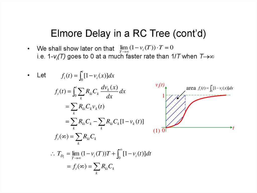
(1 vi (T )) T 0
We shall show later on that Tlim
i.e. 1-vi(T) goes to 0 at a much faster rate than 1/T when T
Let
t
f i (t ) [1 vi ( x)]dx
0
dv ( x)
f i (t ) Rki Ck k
dx
0
dx
k
t
vi(t)
area
t
f i (t ) [1 vi ( x)]dx
0
1
Rki Ck v k (t )
k
Rki Ck Rki Ck [1 vk (t )]
k
f i ( ) Rki Ck
k
(1) 0
k
TDi lim (1 vi (T ))T [1 vi (t )]dt
T
0
f i ( ) Rki Ck
k
t
25. Some Definitions For Signal Bound Computation
Let Tp Rkk Ckk
Recall TDi Rki Ck
k
TRi ( Rki2 Ck ) Rii
k
Then,
TRi TDi Tp
(since Rkk Rki & Rii Rki )
26. Signal Bounds in RC Trees
Theorem
Lower bounds
t 0
0
vi (t ) 1
1
TDi
t 0 (non - trivial when t TDi TRi )
t TRi
TDi
Tp
(T p TRi )
e
Tp
e
t
Tp
t Tp TRi
Upper bounds
1
TDi t
t 0
Tp
v i (t )
1
TRi
Tp
(TDi TRi )
e
TRi
e
t
TRi
t TDi TRi
27. Delay Bounds in RC Trees
Lower bounds :t TDi T p 1 vi (t )
t TDi TRi TRi ln
TRi
T p 1 vi (t )
when vi (t ) 1
TRi
when vi (t ) 1
TDi
Tp
Upper bounds :
t
TDi
1 vi (t )
TRi
TDi
t T p TRi T p ln
T p 1 vi (t )
Tp
28. Computation of Elmore Delay & Delay Bounds in RC Trees
Computation of Elmore Delay & Delay Boundsin RC Trees
• Let C(Tk) be total capacitance of subtree rooted at k
• Elmore delay
TDi
R
k pi
k
C (Tk )
upper bound :
T p Rk C (Tk )
k
lower bound :
TRi Rki2
k
Ck
Rii
* all three formula can be computed in linear tim e recursivel y in a bottom - up
fashion
29. Comments on Elmore Delay Model
• Advantages– Simple closed-form expression
• Useful for interconnect optimization
– Upper bound of 50% delay [Gupta et al., DAC’95, TCAD’97]
• Actual delay asymptotically approaches Elmore delay as input
signal rise time increases
– High fidelity [Boese et al., ICCD’93],[Cong-He, TODAES’96]
• Good solutions under Elmore delay are good solutions under
actual (SPICE) delay
30. Comments on Elmore Delay Model
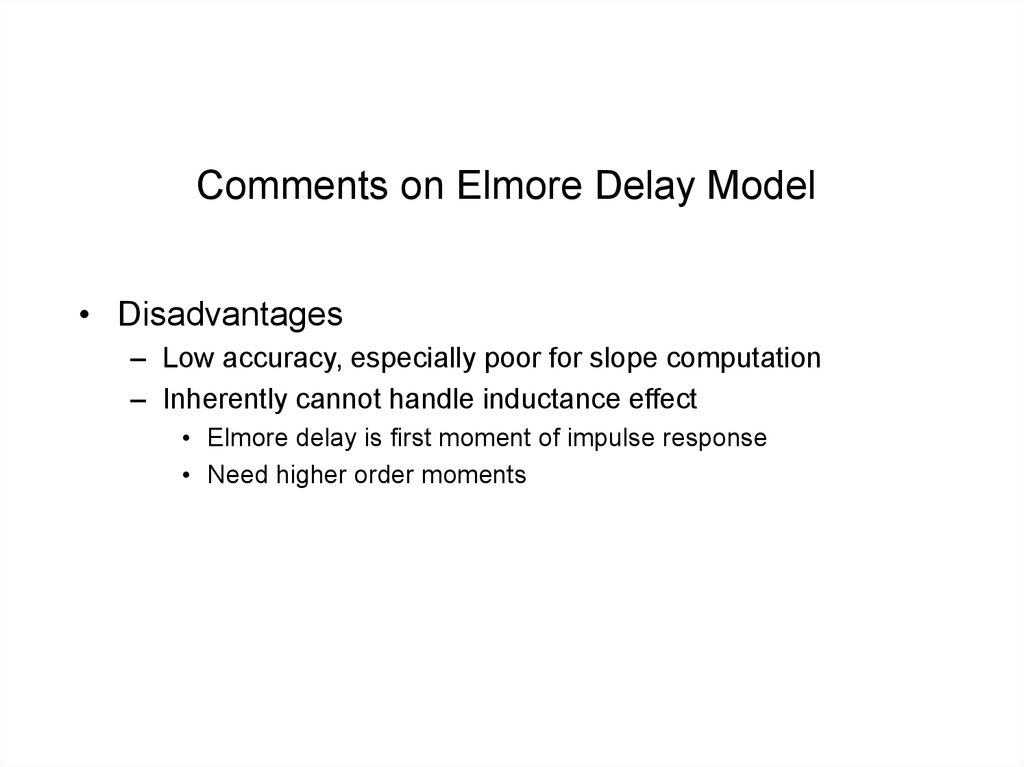
• Disadvantages– Low accuracy, especially poor for slope computation
– Inherently cannot handle inductance effect
• Elmore delay is first moment of impulse response
• Need higher order moments
31. Chapter 7.2 Higher-order Delay Model
32. Time Moments of Impulse Response h(t)
Definition of moments
L
h(t )
H ( s)
0
0
H ( s) h(t )e st dt
1
i
h(t ) ( st ) dt
i 0 i!
1
i
( s) h(t ) t i dt
0
i 0 i!
1
i
i-th moment
mi ( 1) h(t ) t i dt
0
i!
Note that m1 = Elmore delay when h(t) is monotone voltage response of
impulse input
33. Pade Approximation
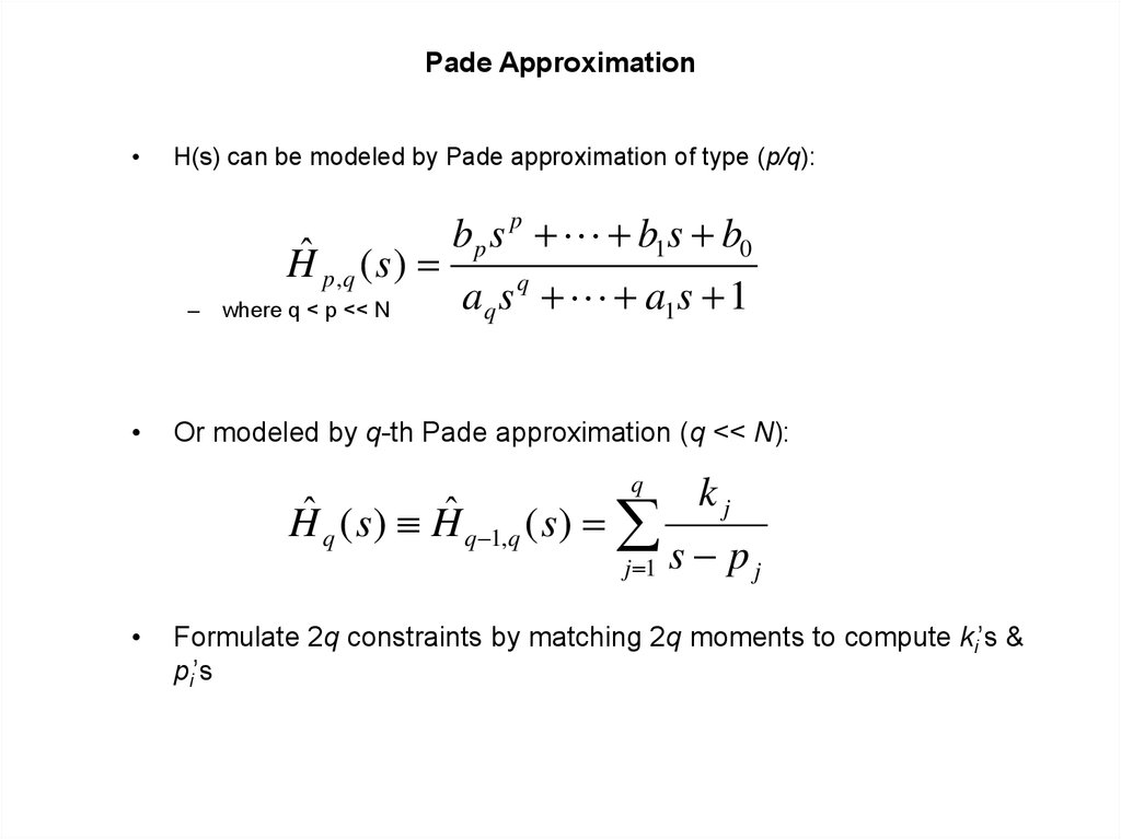
H(s) can be modeled by Pade approximation of type (p/q):
Hˆ p ,q ( s )
–
where q < p << N
bp s p b1s b0
aq s q a1s 1
Or modeled by q-th Pade approximation (q << N):
q
kj
ˆ
ˆ
H q ( s ) H q 1,q ( s )
j 1 s p j
Formulate 2q constraints by matching 2q moments to compute ki’s &
pi’s
34. General Moment Matching Technique
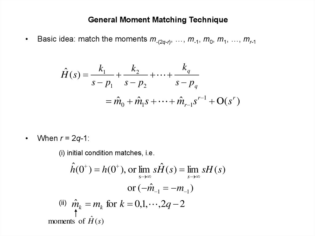
Basic idea: match the moments m-(2q-r), …, m-1, m0, m1, …, mr-1
Hˆ ( s)
kq
k1
k2
s p1 s p2
s pq
mˆ 0 mˆ 1s mˆ r 1s r 1 ( s r )
When r = 2q-1:
(i) initial condition matches, i.e.
hˆ(0 ) h(0 ), or lim sHˆ ( s ) lim sH ( s )
s
s
or ( mˆ 1 m 1 )
(ii)
ˆ k mk for k 0,1, ,2q 2
m
moments of Hˆ ( s)
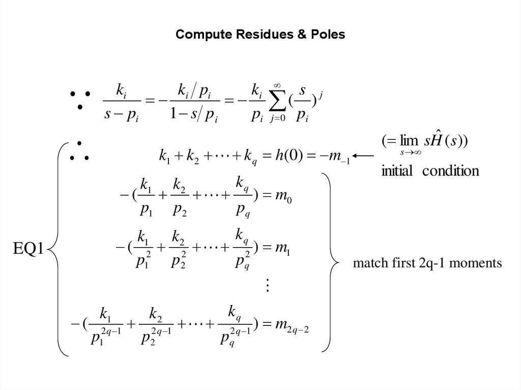
35. Compute Residues & Poles
Compute Residues & Poleski
ki pi
ki
s pi
1 s pi
pi
s j
( )
j 0 pi
k1 k 2 k q h(0) m 1
kq
k1 k 2
(
) m0
p1 p2
pq
EQ1
kq
k1 k 2
( 2 2 2 ) m1
p1 p2
pq
kq
k1
k2
( 2 q 1 2 q 1 2 q 1 ) m2 q 2
p1
p2
pq
( lim sHˆ ( s ))
s
initial condition
match first 2q-1 moments
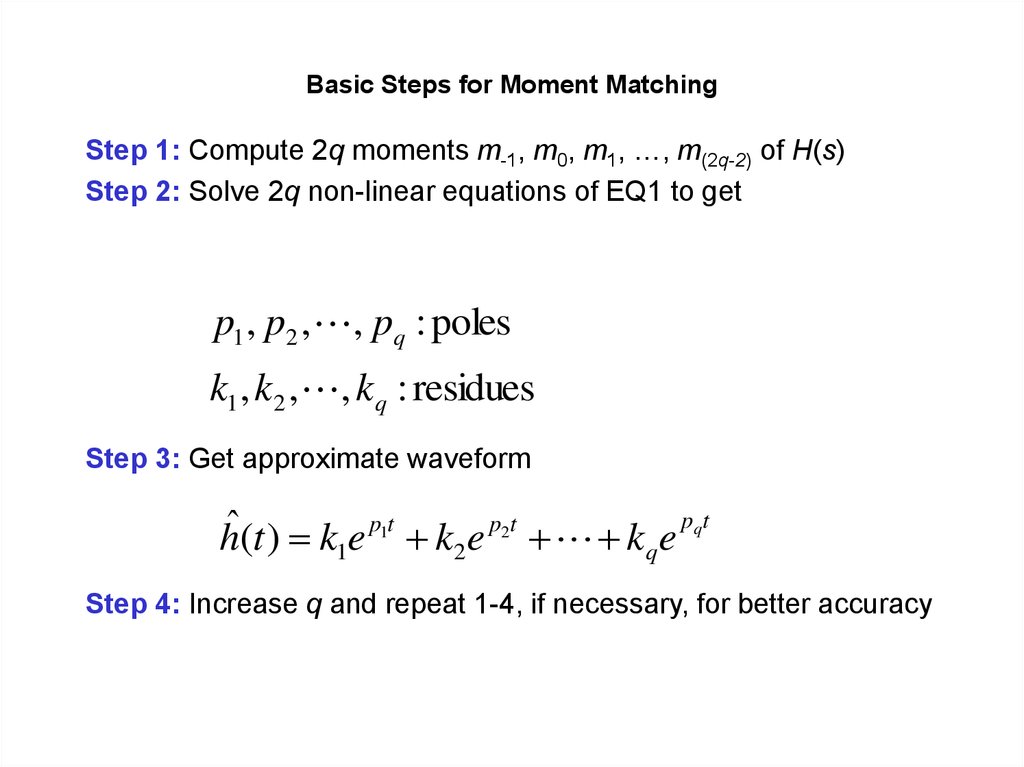
36. Basic Steps for Moment Matching
Step 1: Compute 2q moments m-1, m0, m1, …, m(2q-2) of H(s)Step 2: Solve 2q non-linear equations of EQ1 to get
p1 , p2 , , pq : poles
k1 , k2 , , kq : residues
Step 3: Get approximate waveform
pq t
p1t
p2 t
ˆ
h(t ) k1e k2e kq e
Step 4: Increase q and repeat 1-4, if necessary, for better accuracy
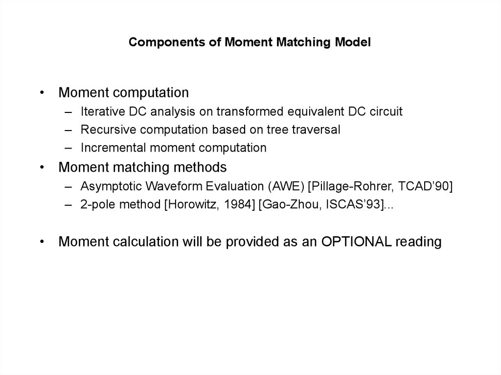
37. Components of Moment Matching Model
• Moment computation– Iterative DC analysis on transformed equivalent DC circuit
– Recursive computation based on tree traversal
– Incremental moment computation
• Moment matching methods
– Asymptotic Waveform Evaluation (AWE) [Pillage-Rohrer, TCAD’90]
– 2-pole method [Horowitz, 1984] [Gao-Zhou, ISCAS’93]...
• Moment calculation will be provided as an OPTIONAL reading
38. Chapter 7 Interconnect Delay
7.1 Elmore Delay7.2 High-order model and moment matching
7.3 Stage delay calculation
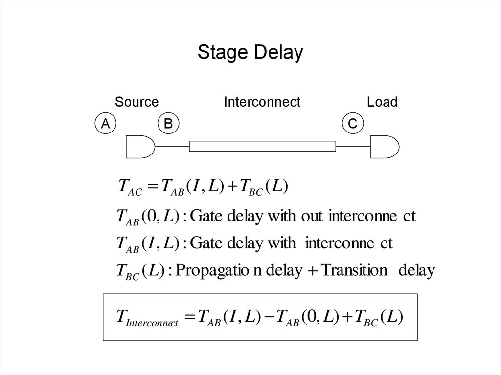
39. Stage Delay
SourceA
Interconnect
B
Load
C
TAC TAB ( I , L) TBC ( L)
TAB (0, L) : Gate delay with out interconne ct
TAB ( I , L) : Gate delay with interconne ct
TBC ( L) : Propagatio n delay Transition delay
TInterconnect TAB ( I , L) TAB (0, L) TBC ( L)
40. Modeling of Capacitive Load
• First-order approximation: the driver sees thetotal capacitance of wires and sinks
• Problem: Ignore shielding effect of resistance
pessimistic approximation as driving point
admittance
• Transform interconnect circuit into a p-model
[O’Brian-Savarino, ICCAD’89]
– Problem: cannot be easily used with most device
models
• Compute effective capacitance from p-model
[Qian-Pullela-Pileggi, TCAD’94]
41. P-Model [O’Brian-Savarino, ICCAD’89]
• Moment matching again!• Consider the first three moments of driving point
admittance (moments of response current caused by
an applied unit impulse)
• Current in the downstream of node k
I k ( s)
C sV (s)
j Tk
j
j
Yk ( s ) I k ( s ) / Vin ( s )
Yk ( s )
C sH
j Tk
j
j
( s)
( i ) i 1
C
s
(
1
m
s
m
s
)
C
m
j
j j s
j Tk
(1)
j
( 2) 2
j
i 1 j Tk
42. Driving-Point Admittance Approximations
• Driving-point admittance = Sum of voltage momentweighted subtree capacitanceyk( i )
( i 1)
C
m
j j
j Tk
Yk ( s ) yk( i ) s i
i 1
• Approximation of the driving point admittance at the
driver
Y (s )
General RC Tree:
lumped RC elements,
distributed RC lines
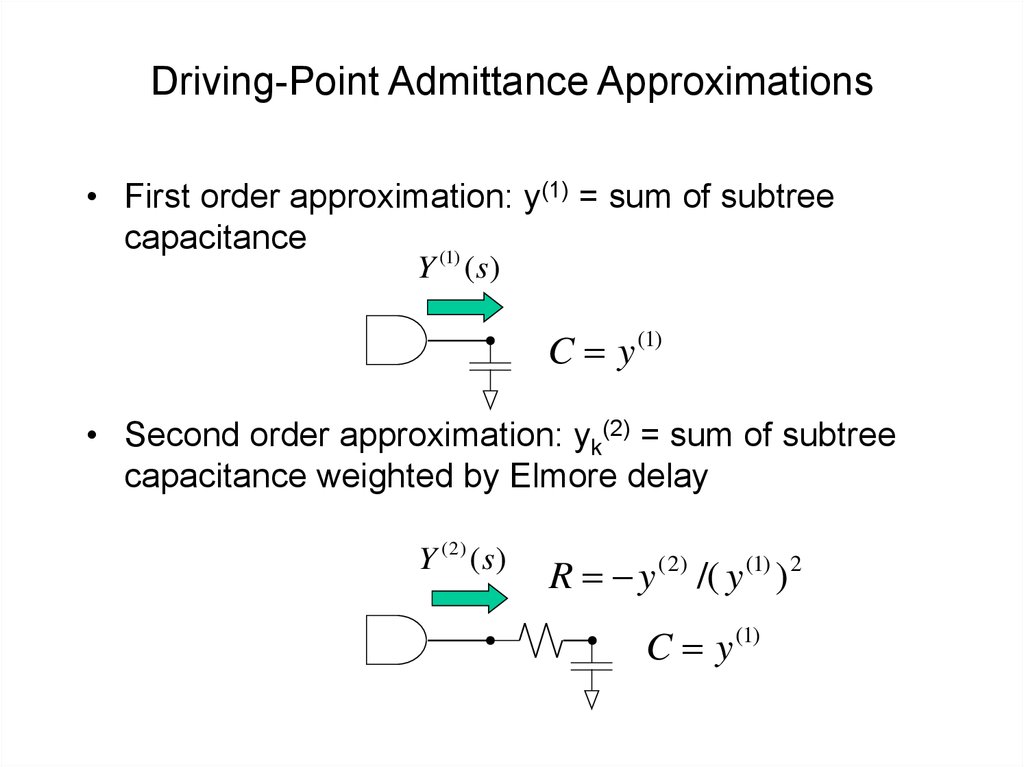
43. Driving-Point Admittance Approximations
• First order approximation: y(1) = sum of subtreecapacitance
(1)
Y ( s)
C y
(1)
• Second order approximation: yk(2) = sum of subtree
capacitance weighted by Elmore delay
Y ( 2) ( s)
R y ( 2) /( y (1) ) 2
C y (1)
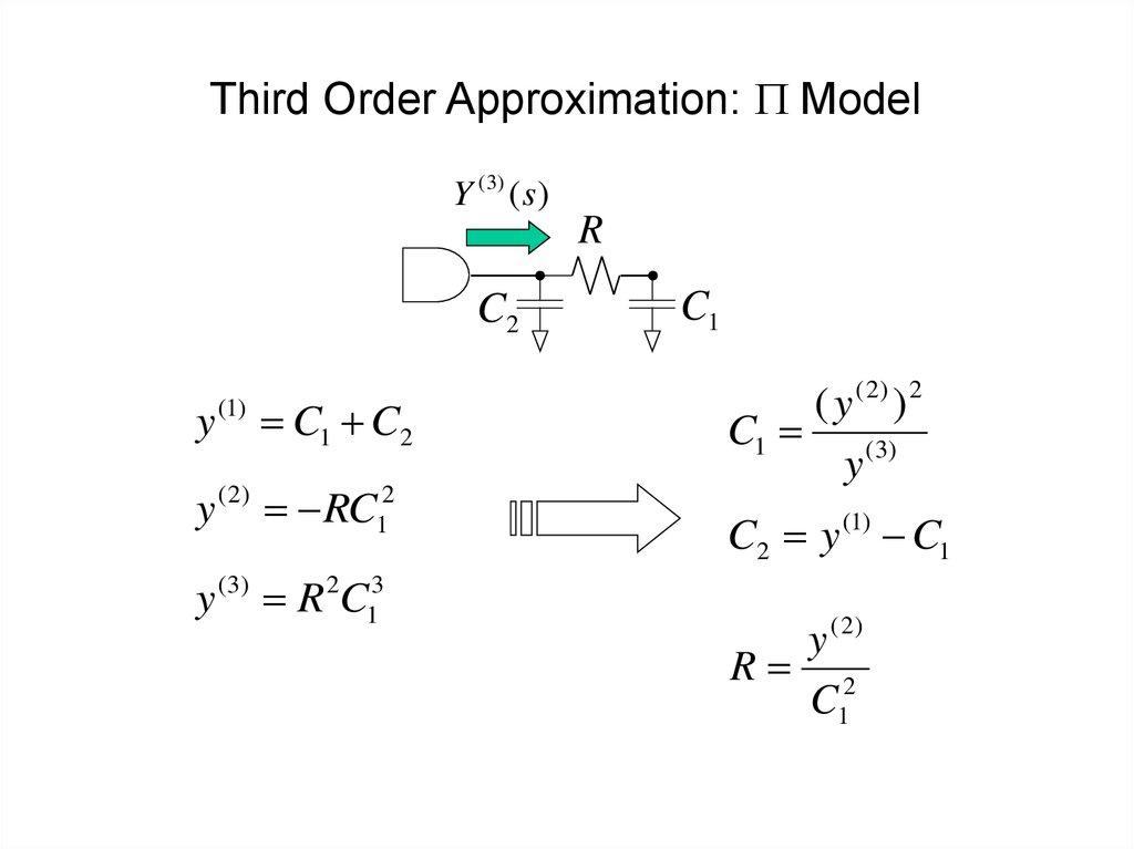
44. Third Order Approximation: P Model
Y ( 3) ( s )R
C2
y
(1)
C1 C2
y ( 2) RC12
y (3) R 2C13
C1
( y ( 2) ) 2
C1 (3)
y
C2 y (1) C1
y ( 2)
R 2
C1
45. Current Moment Computation
• Similar to the voltage moment computation• Iterative tree traversal:
– O(n) run-time, O(n) storage
• Bottom-up tree traversal:
– O(n) run-time
– Can achieve O(k) storage if we impose order of traversal,
k = max degree of a node
– O’Brian and Savarino used bottom-up tree traversal
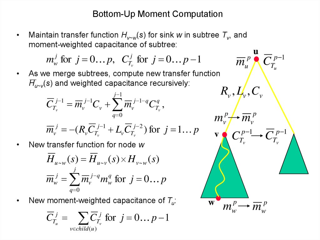
46. Bottom-Up Moment Computation
Maintain transfer function Hv~w(s) for sink w in subtree Tv, and
moment-weighted capacitance of subtree:
m for j 0 p, C for j 0 p 1
j
w
j
Tv
m
As we merge subtrees, compute new transfer function
Hu~v(s) and weighted capacitance recursively:
j 1
CTvj 1 mvj 1Cv mvj 1 q CTqv ,
q 0
mvj ( Rv CTvj 1 Lv CTvj 2 ) for j 1 p
u
p
u
Rv , Lv , Cv
mvp
v
New transfer function for node w
CTpu 1
mvp
CTpv 1
CTpv 1
H u ~ w ( s) H u ~ v ( s) H v ~ w ( s)
j
m mvj q mwq for j 0 p
j
w
q 0
New moment-weighted capacitance of Tu:
CTuj
j
C
Tv for j 0 p 1
v child ( u )
w
mwp
mwp
47. Current Moment Computation Rule #1
yU(1) y D(1) CYU (s)
YD (s)
C
yU( 2 ) y D( 2 )
yU(3) y D(3)
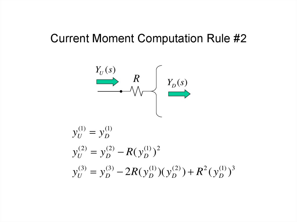
48. Current Moment Computation Rule #2
YU (s)R
YD (s)
yU(1) y D(1)
yU( 2) y D( 2) R( y D(1) ) 2
yU(3) y D(3) 2 R( y D(1) )( y D( 2) ) R 2 ( y D(1) )3
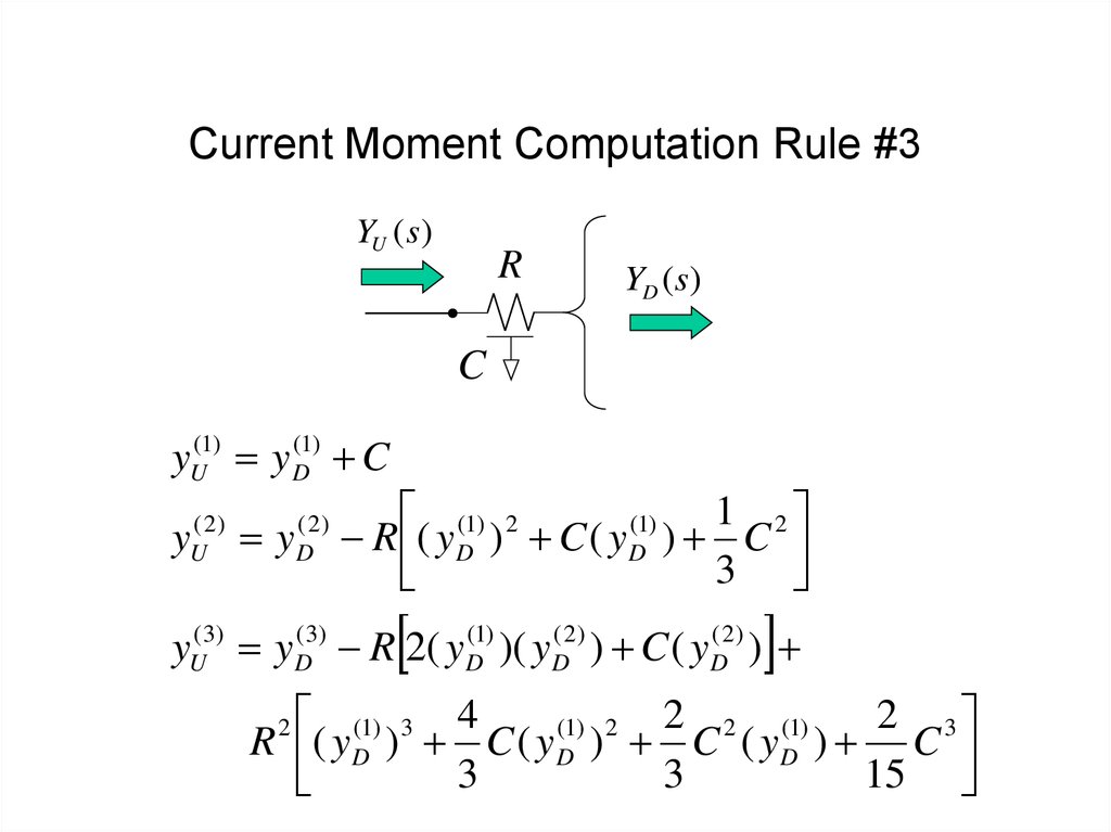
49. Current Moment Computation Rule #3
YU (s)R
YD (s)
C
yU(1) y D(1) C
( 2)
U
y
y
( 2)
D
1 2
(1) 2
(1)
R ( y D ) C ( y D ) C
3
yU(3) y D(3) R 2( y D(1) )( y D( 2) ) C ( y D( 2) )
2 2 (1)
2 3
(1) 3 4
(1) 2
R ( y D ) C ( y D ) C ( y D ) C
3
3
15
2
50. Current Moment Computation Rule #4 (Merging of Sub-trees)
BYD1 ( s)
YU (s)
(1)
yU(1) y Di
i 1
B
B Branches
( 2)
yU( 2 ) y Di
i 1
YDB (s)
B
( 3)
U
y
( 3)
y Di
i 1
51. Example: Uniform Distributed RC Segment
Purely capacitiveTAB/TAB(0)
Wide metal (distributive)
Wide metal (p)
Wide metal (lumped RC)
Narrow metal (p)
Narrow metal (distributive)
Narrow metal (lumped RC)
Cload/Cmax
52. Why Effective Capacitance Model?
• The p-model is incompatible with existing empirical devicemodels
– Mapping of 4D empirical data is not practical from a storage
or run-time point of view
• Convert from a p-model to an effective capacitance
model for compatibility
• Equate the average current in the p-load and the Ceff
load
R
in
C2
C1
in
C eff
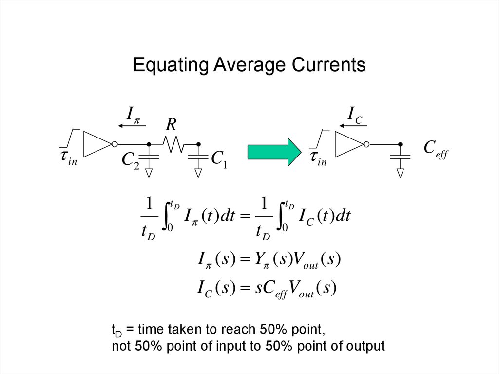
53. Equating Average Currents
Ipin
IC
R
in
C1
C2
1
tD
tD
0
1
Ip (t )dt
tD
tD
0
I C (t )dt
Ip ( s) Yp ( s)Vout ( s)
I C ( s) sCeff Vout ( s)
tD = time taken to reach 50% point,
not 50% point of input to 50% point of output
C eff
54. Waveform Approximation for Vout(t)
• Quadratic from initial voltage (Vi = VDD for falling waveform) to20% point, linear to the 50% point
Vi ct 2
Vout (t )
a b(t t x )
0 t tx
tx t tD
• Voltage waveform and first derivative are continuous at tx
a Vi ct x2
b 2ct x
55. Average Currents in Capacitors
tD1 tx
I C (t )
C
(
2
ct
)
dt
C
(
2
ct
)
dt
eff
eff
x
tx
t D 0
2Ceff c t x
tD
[t D
tx
]
2
2C2 c t x
tx
I C2 (t )
[t D ]
tD
2
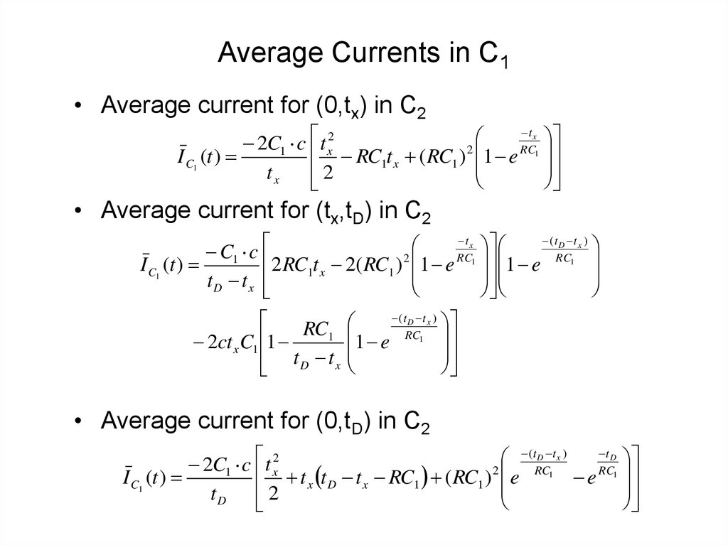
• Average current of C1 is not quite as simple:
– Current due to quadratic current in C2
– Current due to linear current in C2
56. Average Currents in C1
• Average current for (0,tx) in C2t x
2
2C1 c t x
RC1
2
RC1t x ( RC1 ) 1 e
I C1 (t )
tx
2
• Average current for (tx,tD) in C2
t x
( t D t x )
C1 c
RC1
RC1
2
2 RC1t x 2( RC1 ) 1 e
1 e
I C1 (t )
tD tx
RC1
2ct x C1 1
t D t x
( t D t x )
1 e RC1
• Average current for (0,tD) in C2
( t D t x )
t D
2C1 c t x2
RC1
RC1
2
t x t D t x RC1 ( RC1 ) e
I C1 (t )
e
tD 2
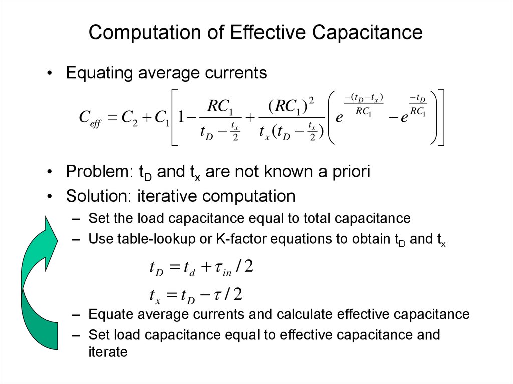
57. Computation of Effective Capacitance
• Equating average currentsCeff
t D
2 ( t D t x )
RC1
( RC1 ) RC1
RC1
C2 C1 1
e
e
tx
tx
t D 2 t x (t D 2 )
• Problem: tD and tx are not known a priori
• Solution: iterative computation
– Set the load capacitance equal to total capacitance
– Use table-lookup or K-factor equations to obtain tD and tx
t D t d in / 2
tx tD / 2
– Equate average currents and calculate effective capacitance
– Set load capacitance equal to effective capacitance and
iterate
58. Stage Delay Computation
• Calculate output waveform at gate– Using Ceff model to model interconnect
• Use the output waveform at gate as the input
waveform for interconnect tree load
• Apply interconnect reduced-order modeling technique
to obtain output waveform at receiver pins







![Elmore Delay of a RC Tree [Rubinstein-Penfield-Horowitz, T-CAD’83] Elmore Delay of a RC Tree [Rubinstein-Penfield-Horowitz, T-CAD’83]](https://cf.ppt-online.org/files1/slide/f/FqOWostp7CQBVEvXLYer4ykJgSmxHn9Gub8N1K/slide-21.jpg)




![P-Model [O’Brian-Savarino, ICCAD’89] P-Model [O’Brian-Savarino, ICCAD’89]](https://cf.ppt-online.org/files1/slide/f/FqOWostp7CQBVEvXLYer4ykJgSmxHn9Gub8N1K/slide-40.jpg)






 Информатика
 Электроника


