


 Электроника
Похожие презентации:


BP560X System Application Notes
1.
BP560X System ApplicationNotes
1
www.bpsemi.com
2.
ContentsPatent
Effect
Typical Applications / Overview
Examples of Design
Considerations of Design
2
www.bpsemi.com
3.
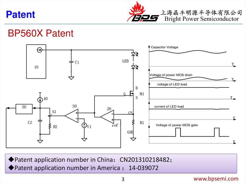
PatentBP560X Patent
Capacitor Voltage
LED
C1
T
10
Voltage of power MOS drain
T
voltage of LED load
D
G
S
40
30
50
T
current of LED load
20
S1
M1
CS
T
C2
R2
V1
R1
ref
Voltage of power MOS gate
GND
T
Patent application number in China CN201310218482
Patent application number in America 14-039072
3
www.bpsemi.com
4.
EffectBP3316D+BP5609 (36V/430mA)
The Ripple is
decreased
No strobe
Io
Vo
+5609
After the current loop is closed, the current and voltage on the LED are
DC
The voltage ripple will be superimposed on the MOSFET
4
www.bpsemi.com
5.
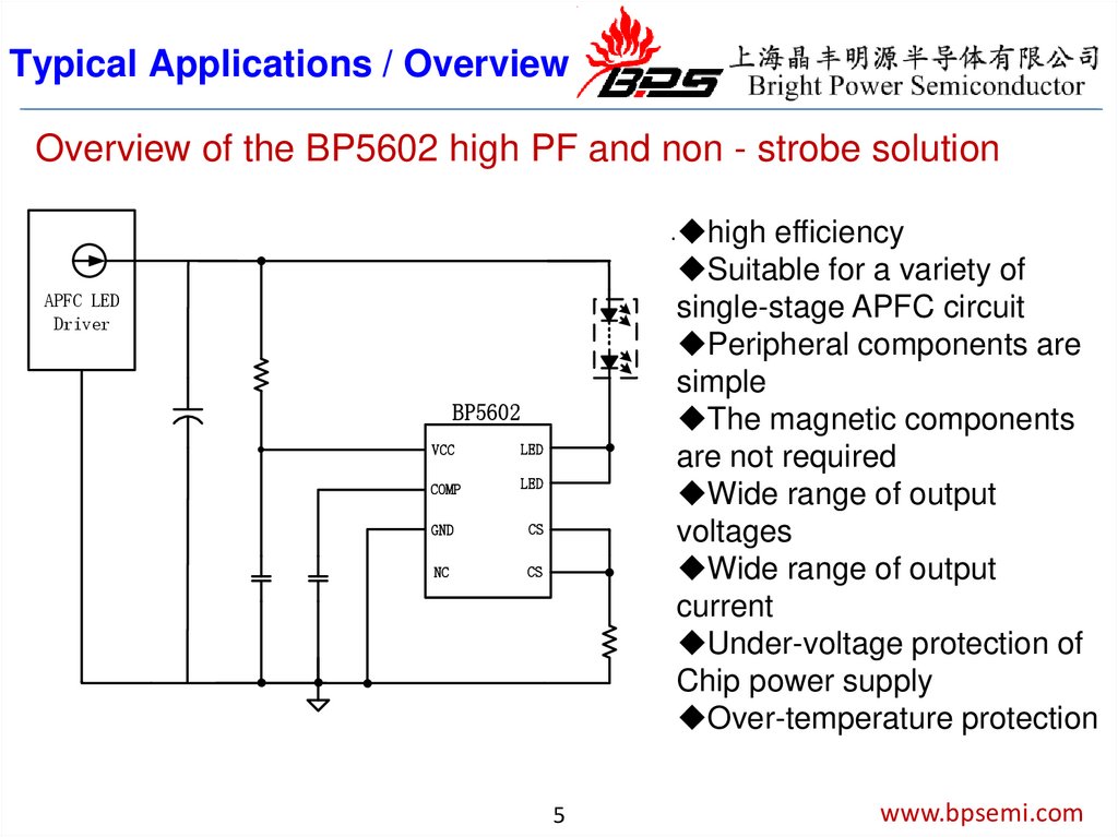
Typical Applications / OverviewOverview of the BP5602 high PF and non - strobe solution
high efficiency
Suitable for a variety of
single-stage APFC circuit
Peripheral components are
simple
The magnetic components
are not required
Wide range of output
voltages
Wide range of output
current
Under-voltage protection of
Chip power supply
Over-temperature protection
APFC LED
Driver
BP5602
VCC
LED
COMP
LED
GND
CS
NC
CS
5
www.bpsemi.com
6.
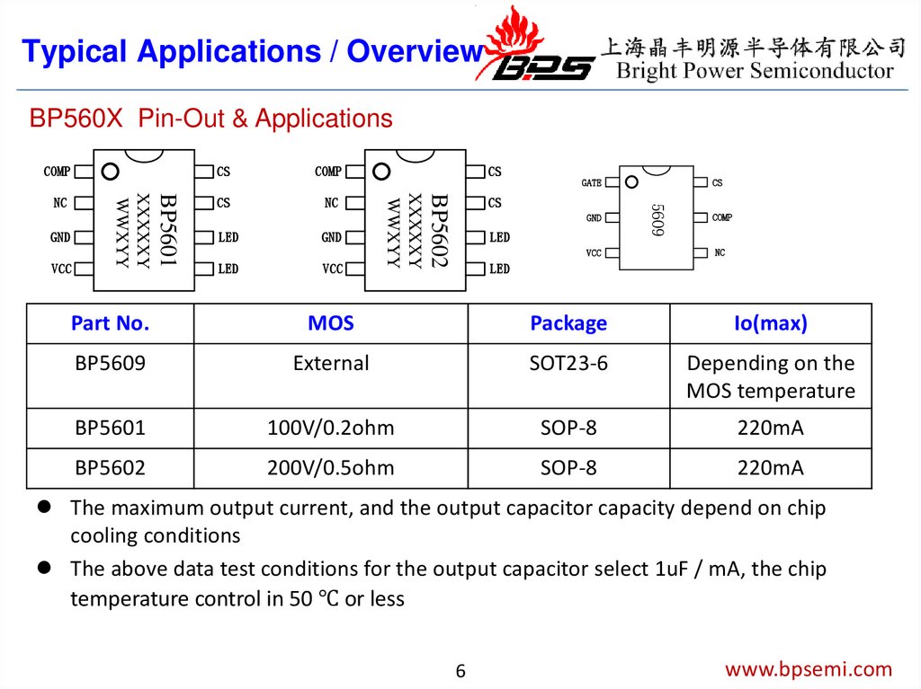
Typical Applications / OverviewBP560X Pin-Out & Applications
COMP
NC
LED
GND
LED
VCC
GATE
CS
GND
LED
VCC
CS
5609
CS
CS
BP5602
COMP
XXXXXY
WWXYY
VCC
BP5601
GND
XXXXXY
WWXYY
NC
CS
COMP
NC
LED
Part No.
MOS
Package
Io(max)
BP5609
External
SOT23-6
Depending on the
MOS temperature
BP5601
100V/0.2ohm
SOP-8
220mA
BP5602
200V/0.5ohm
SOP-8
220mA
The maximum output current, and the output capacitor capacity depend on chip
cooling conditions
The above data test conditions for the output capacitor select 1uF / mA, the chip
temperature control in 50 ℃ or less
6
www.bpsemi.com
7.
Typical Applications / OverviewLED+
BP5609 Typical Applications (Vo=36V;Io=440mA)
L
N
LED-
LED
R1
27K
V in +
BP3316D
Q1
C1
V in -
U2
+
1
GATE CS
6
BP5609
C2
4.7uF/25V
7
2
GND COMP 5
3
VCC
NC
4
Rs1
1.0R
Rs2
1.0R
C3
4.7uF/16V
www.bpsemi.com
8.
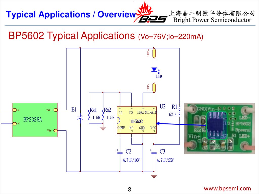
Typical Applications / OverviewLED+
BP5602 Typical Applications (Vo=76V;Io=220mA)
+
BP2328A
1.5R
Rs2
CS
CS
1.5R
U2
DRAIN DRAIN
R1
62 K
BP5602
+
NC
GND
3
1
COMP
2
N
V in -
5
Rs1
C2
4.7uF/16V
8
VCC
4
E1
6
V in +
7
L
8
LED-
LED
+
C3
4.7uF/25V
www.bpsemi.com
9.
Examples of DesignBP3316D+BP5609 36V/430mA
Load regulation in 220Vac
424
Output current mA
Output current mA
Linear adjustment rate of Full load
422
420
418
416
414
80
120
160
200
240
280
422
421
420
419
418
417
20
Input voltage V
28
32
36
40
output voltage V
PF
efficiency of Full load
1
84
83
0,98
82
0,96
PF
effectiveness %
24
0,94
81
BP5609AA
80
79
0,92
0,9
80
120
160
200
Input voltage V
240
280
80
120
160
200
240
280
Input voltage V
no-affect to the linear load regulation,and PF / THD; efficiency decreased by about 2
percentage points 。
www.bpsemi.com
9
10.
Examples of DesignSelection of pre-output capacitor
According to the output current, it is recommended to select the preoutput capacitor of 1uF / mA
Capacitance is too large,when from open or normal work to short-circuit it
is more likely to burn, and it is not helpful to the system efficiency
The pre-output capacitor is larger, the ripple amplitude is lower, the
temperature of chip is lower
The per-input capacitance is larger, the efficiency of the system loss
with the BP560X is lower
10
www.bpsemi.com
11.
Examples of DesignPower Loss VS Output Cap
1,4
Input power loss W
1,2
1
0,8
0,6
0,4
0,2
0
0
220
440
660
880
1100
1320
The output capacitor(uF)
BP3316D + BP5609 36V / 430mA, the output capacitor 440uF, the loss of
about 2 to 3% efficiency
11
www.bpsemi.com
12.
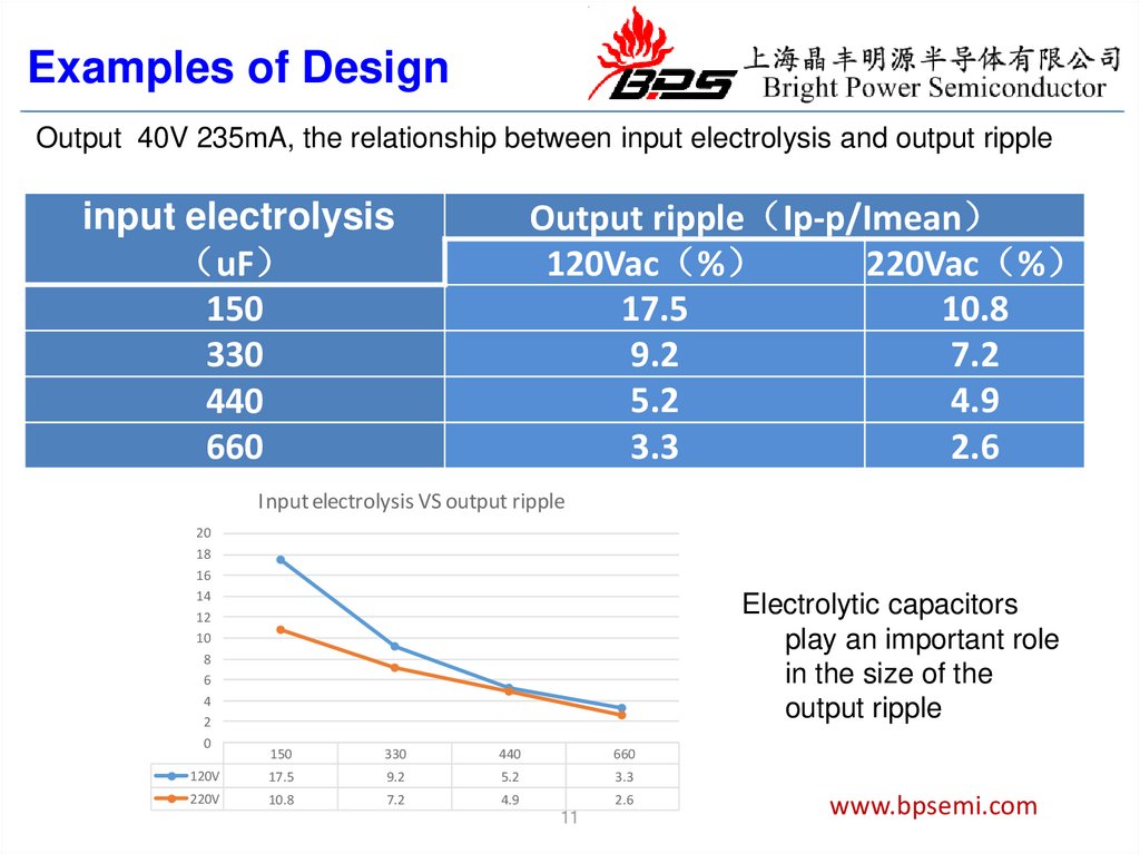
Examples of DesignOutput 40V 235mA, the relationship between input electrolysis and output ripple
Output ripple Ip-p/Imean
120Vac %
220Vac %
17.5
10.8
9.2
7.2
5.2
4.9
3.3
2.6
input electrolysis
uF
150
330
440
660
Input electrolysis VS output ripple
20
18
16
14
12
10
8
6
4
2
0
Electrolytic capacitors
play an important role
in the size of the
output ripple
150
330
440
660
120V
17.5
9.2
5.2
3.3
220V
10.8
7.2
4.9
2.6
11
www.bpsemi.com
13.
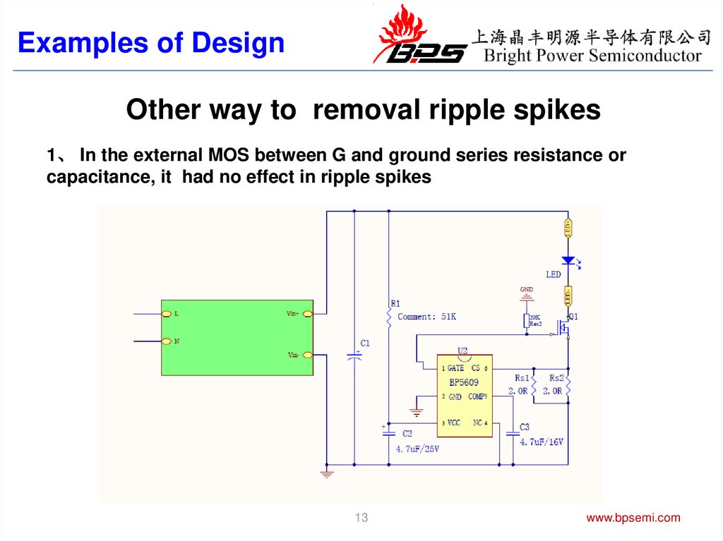
Examples of DesignOther way to removal ripple spikes
1、 In the external MOS between G and ground series resistance or
capacitance, it had no effect in ripple spikes
13
www.bpsemi.com
14.
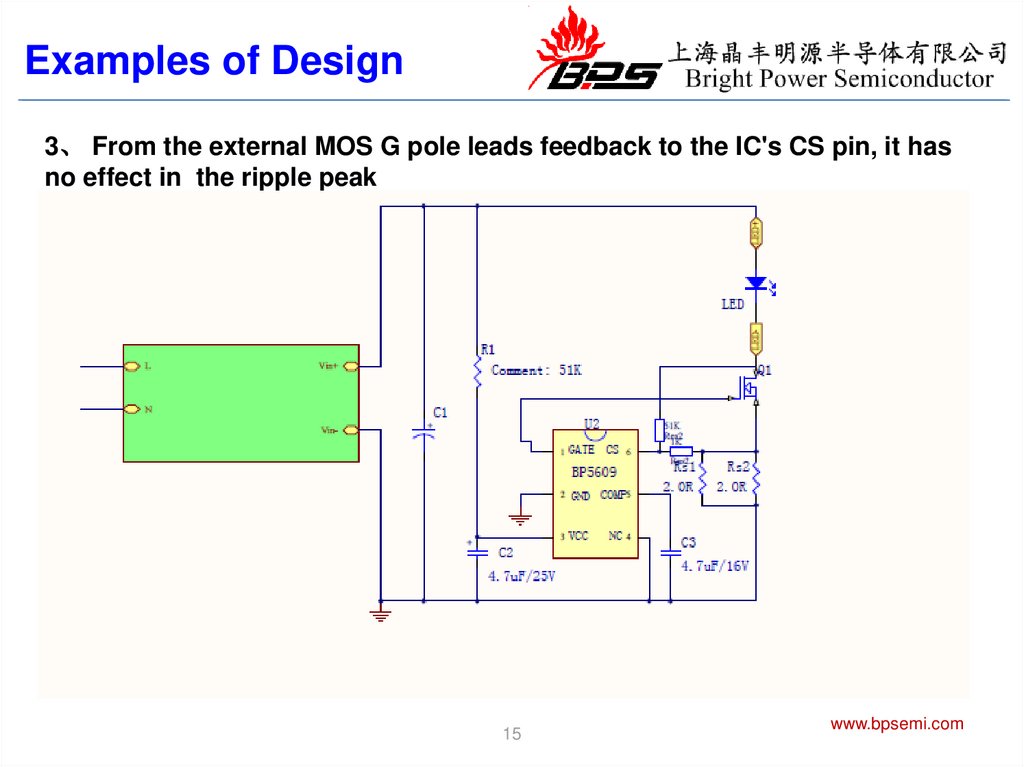
Examples of Design3、 From the external MOS G pole leads feedback to the IC's CS pin, it has
no effect in the ripple peak
15
www.bpsemi.com
15.
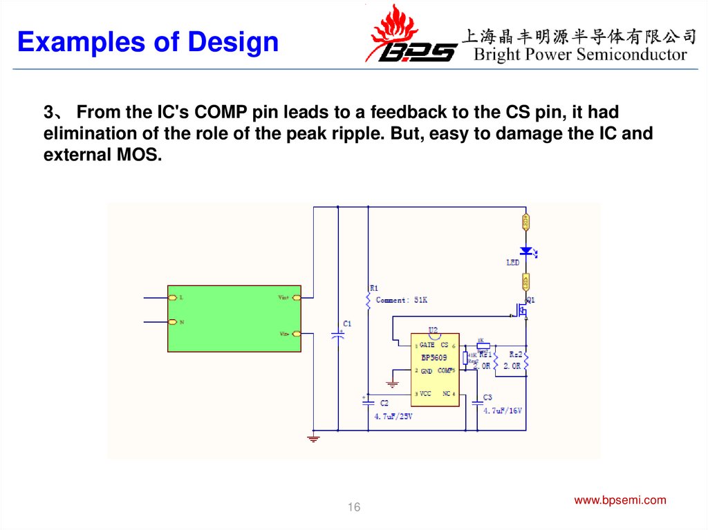
Examples of Design3、 From the IC's COMP pin leads to a feedback to the CS pin, it had
elimination of the role of the peak ripple. But, easy to damage the IC and
external MOS.
16
www.bpsemi.com
16.
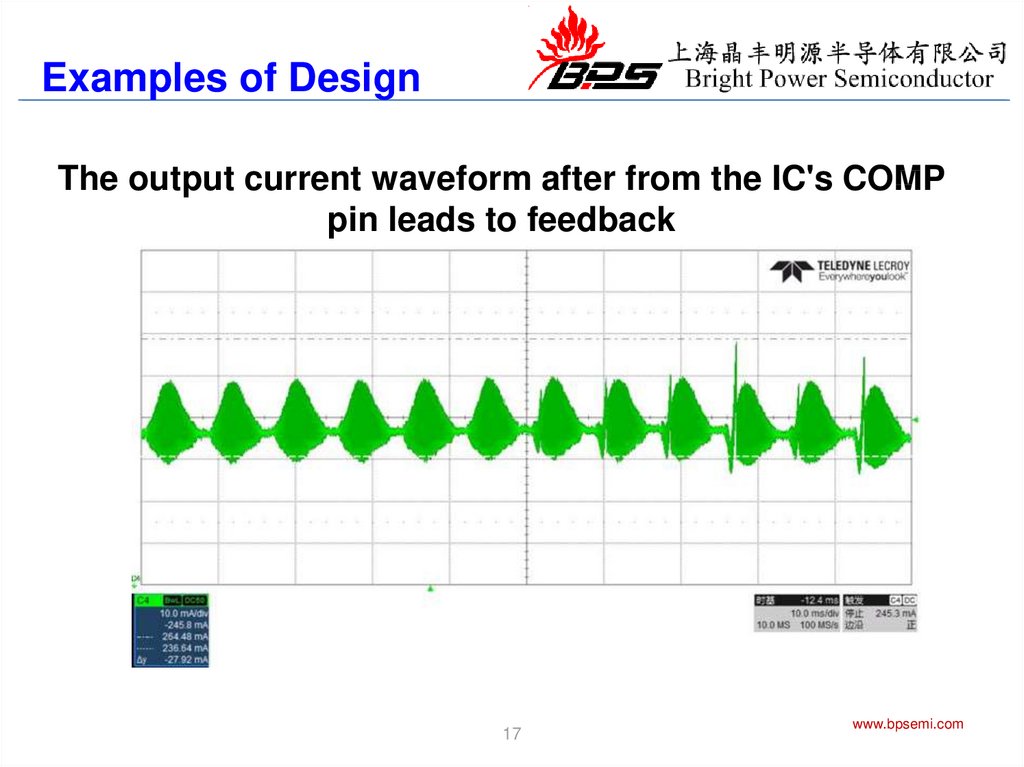
Examples of DesignThe output current waveform after from the IC's COMP
pin leads to feedback
17
www.bpsemi.com
17.
Examples of DesignPre-APFC'S capacitor parameters requirements
Pre-APFC'S COMP capacitor capacitance should not be greater than 1uF,
otherwise the LED will flash
17
www.bpsemi.com
18.
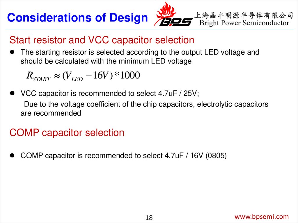
Considerations of DesignStart resistor and VCC capacitor selection
The starting resistor is selected according to the output LED voltage and
should be calculated with the minimum LED voltage
RSTART (VLED 16V ) *1000
VCC capacitor is recommended to select 4.7uF / 25V;
Due to the voltage coefficient of the chip capacitors, electrolytic capacitors
are recommended
COMP capacitor selection
COMP capacitor is recommended to select 4.7uF / 16V (0805)
18
www.bpsemi.com
19.
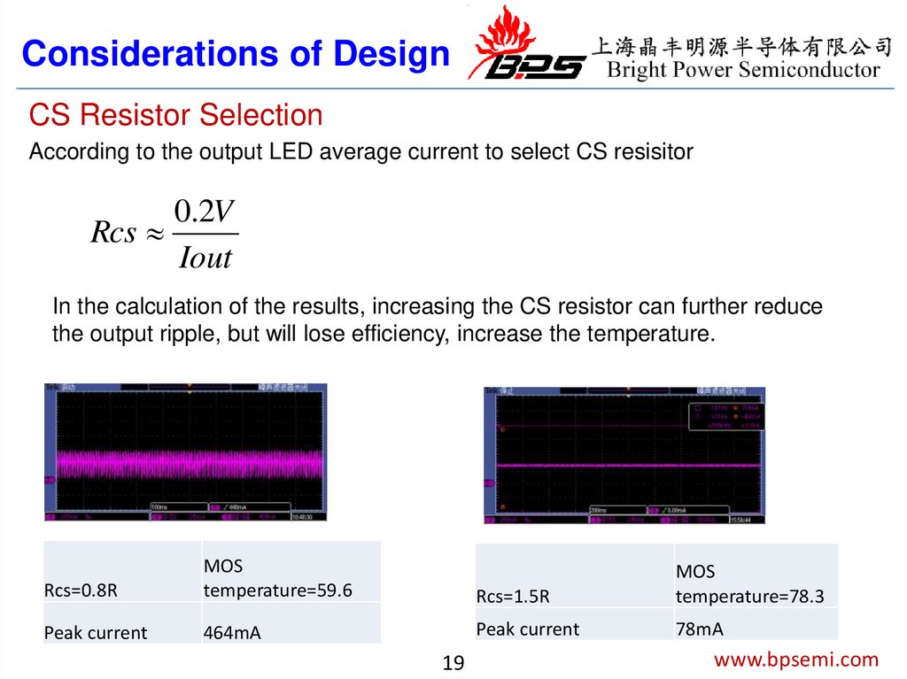
Considerations of DesignCS Resistor Selection
According to the output LED average current to select CS resisitor
0.2V
Rcs
Iout
In the calculation of the results, increasing the CS resistor can further reduce
the output ripple, but will lose efficiency, increase the temperature.
Rcs=0.8R
MOS
temperature=59.6
Rcs=1.5R
MOS
temperature=78.3
Peak current
464mA
Peak current
78mA
19
www.bpsemi.com
20.
Considerations of DesignRepeated switch
Repeated switch does not appear repeatedly start phenomenon
Vds
Vcc
Vo
Io
20
www.bpsemi.com
21.
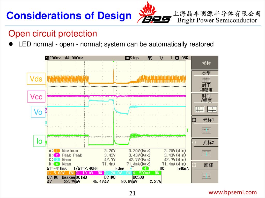
Considerations of DesignOpen circuit protection
LED normal - open - normal; system can be automatically restored
Vds
Vcc
Vo
Io
21
www.bpsemi.com
22.
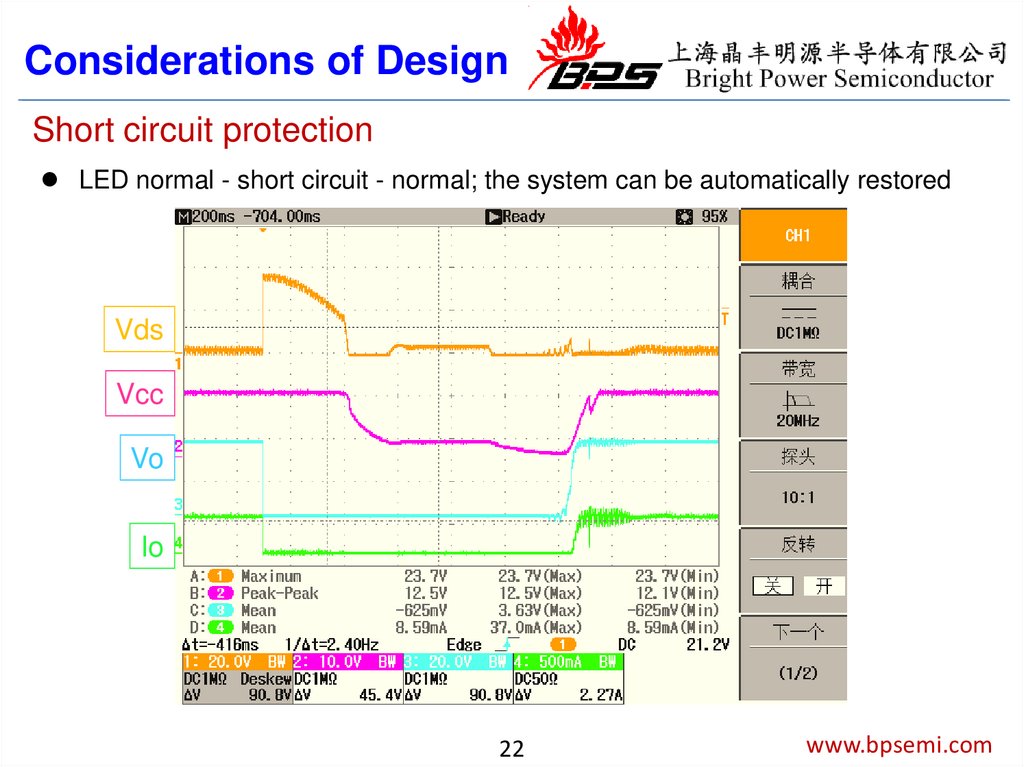
Considerations of DesignShort circuit protection
LED normal - short circuit - normal; the system can be automatically restored
Vds
Vcc
Vo
Io
22
www.bpsemi.com
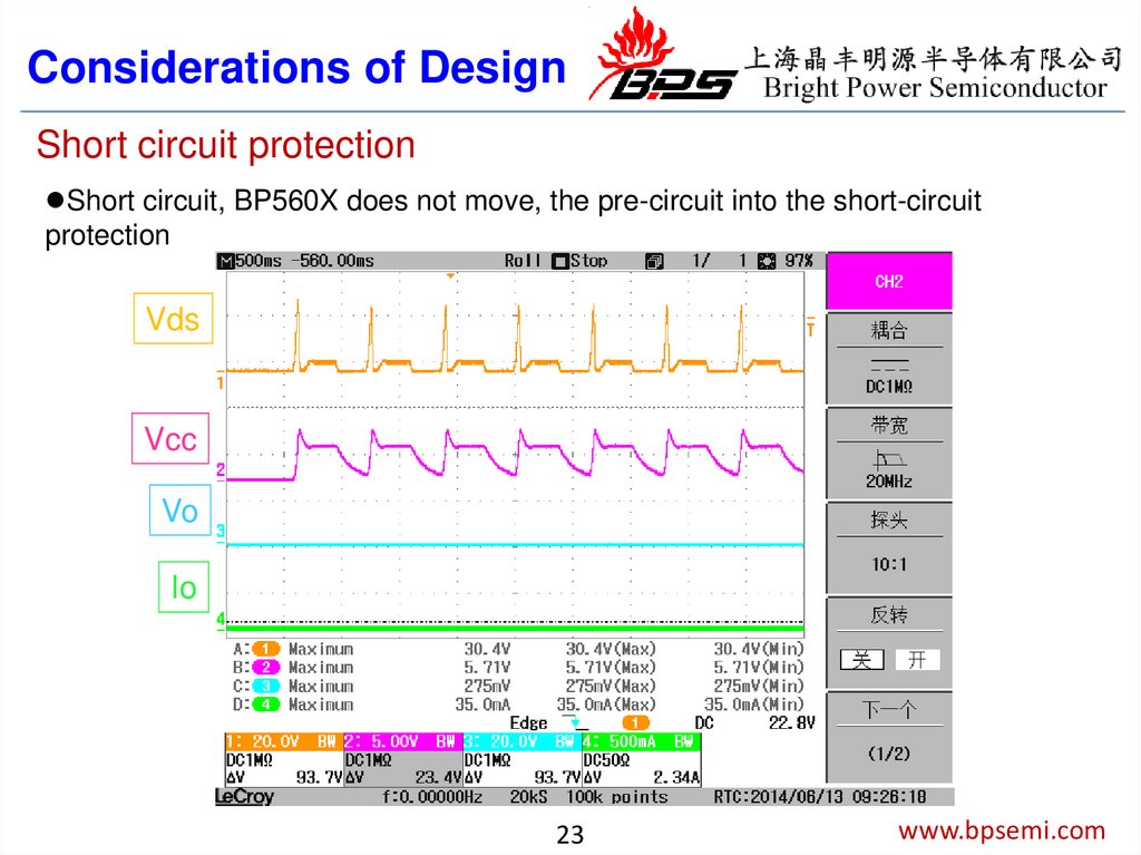
23.
Considerations of DesignShort circuit protection
Short circuit, BP560X does not move, the pre-circuit into the short-circuit
protection
Vds
Vcc
Vo
Io
23
www.bpsemi.com
24.
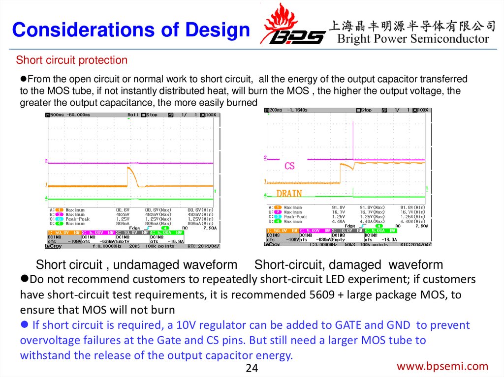
Considerations of DesignShort circuit protection
From the open circuit or normal work to short circuit, all the energy of the output capacitor transferred
to the MOS tube, if not instantly distributed heat, will burn the MOS , the higher the output voltage, the
greater the output capacitance, the more easily burned
CS
DRAIN
Short circuit , undamaged waveform Short-circuit, damaged waveform
Do not recommend customers to repeatedly short-circuit LED experiment; if customers
have short-circuit test requirements, it is recommended 5609 + large package MOS, to
ensure that MOS will not burn
If short circuit is required, a 10V regulator can be added to GATE and GND to prevent
overvoltage failures at the Gate and CS pins. But still need a larger MOS tube to
withstand the release of the output capacitor energy.
www.bpsemi.com
24
25.
Considerations of DesignLayout
Increase Drain's
copper area,
improve cooling
capacity
GND
GND Leakage copper to
prevent leakage of high
voltage on the COMP
COMP
capacitance
25
www.bpsemi.com