


 Электроника
Похожие презентации:


Simulation with Conditions
1.
DBHitek 180nm BCD ProcesseFuse Cell Array _Simulation_Schematic
DOUT_Buffer_Unit _Schematic
DOUT_Buffer_Unit_8C_Schematic
2.
DBHitek 180nm BCD ProcesseFuse Cell Array _Simulation_Schematic
Cell_Schematic
Cell1R_8C_Schematic
3.
DBHitek 180nm BCD ProcesseFuse Cell Array _Simulation_Schematic
Cell8R_8C_Schematic
Cell16R_8C_Schematic
4.
DBHitek 180nm BCD ProcesseFuse Cell Array _Simulation_Schematic
SL_Driver _8C_Schematic
SL_Driver_Schematic
5.
DBHitek 180nm BCD ProcesseFuse Cell Array _Simulation_Schematic
WL_Driver_Unit_Schematic
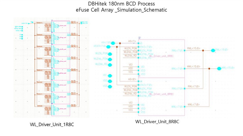
6.
DBHitek 180nm BCD ProcesseFuse Cell Array _Simulation_Schematic
WL_Driver_Unit_1R8C
WL_Driver_Unit_8R8C
7.
DBHitek 180nm BCD ProcesseFuse Cell Array _Simulation_Schematic
Ypre_Decoder_Schematic
8.
DBHitek 180nm BCD ProcesseFuse Cell Array _Simulation_Schematic
Xpre_Decoder_Schematic
9.
DBHitek 180nm BCD ProcesseFuse Cell Array _Simulation_Schematic
BL_LoADb_Schematic
10.
DBHitek 180nm BCD ProcesseFuse Cell Array _Simulation_Schematic
SAENb_Schematic
11.
DBHitek 180nm BCD ProcesseFuse Cell Array _Simulation_Schematic
BL_PCG_Schematic
12.
DBHitek 180nm BCD ProcesseFuse Cell Array _Simulation_Schematic
WL_CTRL_Schematic
13.
DBHitek 180nm BCD ProcesseFuse Cell Array _Simulation_Schematic
CS_Buffer_Schematic
14.
DBHitek 180nm BCD ProcesseFuse Cell Array _Simulation_Schematic
BL_SA_CTRL_Schematic
15.
DBHitek 180nm BCD ProcesseFuse Cell Array _Simulation_Schematic
Control_Logic_Schematic
16.
DBHitek 180nm BCD ProcesseFuse Cell Array _Simulation_Schematic
Core_Schematic
17.
DBHitek 180nm BCD ProcesseFuse Cell Array _Simulation_Schematic
Top_Schematic
18.
DBHitek 180nm BCD ProcesseFuse Cell Array _Simulation_Schematic
Subject:128bit eFuse OTP IP design
Problem statement:creating a convenable circuit that satisfied these specifications
– Supply voltage: VDD=2.2V – VIO=5.5VTemperature:-40C 25 C to 125C
Operating Mode :Program/Program Verify-Read/ReadProgram.
– ReadProgram Verify:10k
– Read Mode :5k {Read_Programmed Cell& Read_Uprogrammed Cell
– Current :<100uA. (Decreasing current from 168.4uA to 100uA
Expected result: Suitable block diagram have to be find out by modifying the above simulation circuits based on the
requirements.
19.
DBHitek 180nm BCD ProcesseFuse Cell Array _Simulation_Schematic
Simulation software :CX-HSPUI -Xftp5 -Crimson Editor
Design & Layout software :VLSI7(VLSI7:177) -Xmanager5[:0.0]
20.
DBHitek 180nm BCD ProcesseFuse Cell Array _Simulation_Schematic