


 Информатика
Похожие презентации:


")


2012 Component Training Ivy Platform Series
1.
2012 Component TrainingIvy Platform Series
Confidential
2.
Ivy 7 Series – Agenda• Platform Structure
CPU feature introduce
Intel 7 series chipset architecture
Critical Power Flow
Clock Distribution
Power Sequence
Problem Debug
Can’t power on
Power auto shutdown
All dots, zero, and no display
Power part
3.
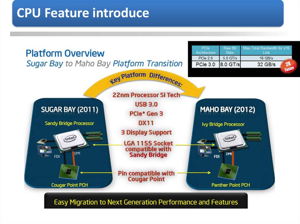
CPU Feature introduce4.
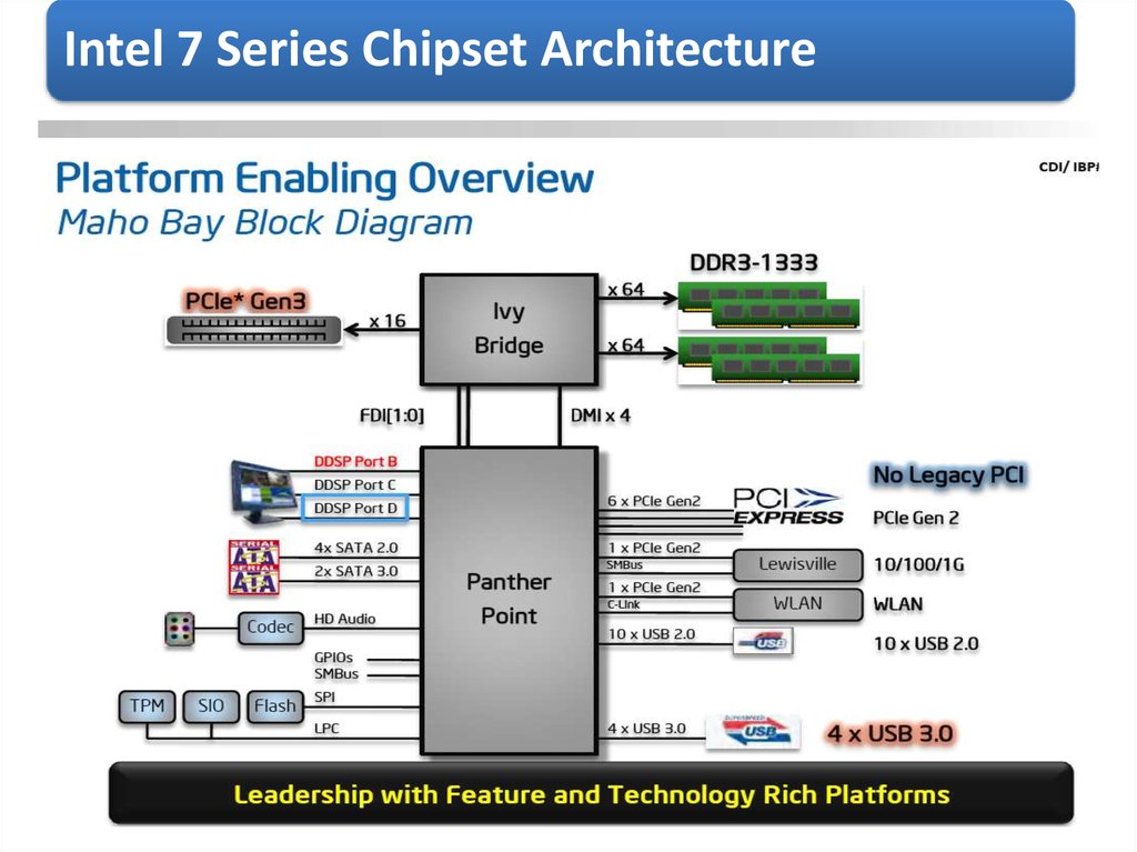
Intel 7 Series Chipset Architecture5.
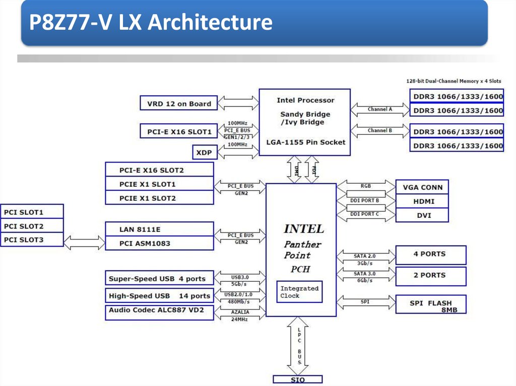
P8Z77-V LX Architecture6.
P8Z77-V DELUXE Architecture7.
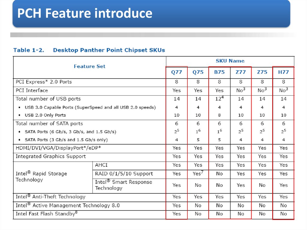
PCH Feature introduce8.
Ivy 7 Series – Agenda• Platform Structure
CPU feature introduce
Intel 7 series chipset architecture
Critical Power Flow
Clock Distribution
Power Sequence
Problem Debug
Can’t power on
Power auto shutdown
All dots, zero, and no display
Power part
9.
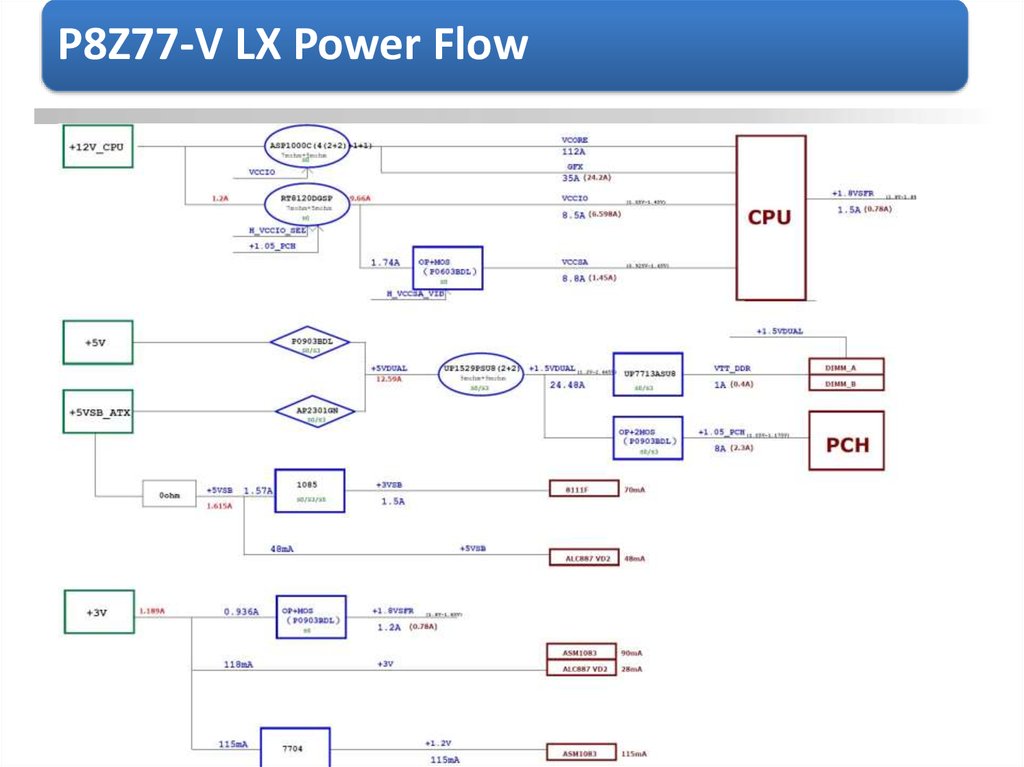
P8Z77-V LX Power Flow10.
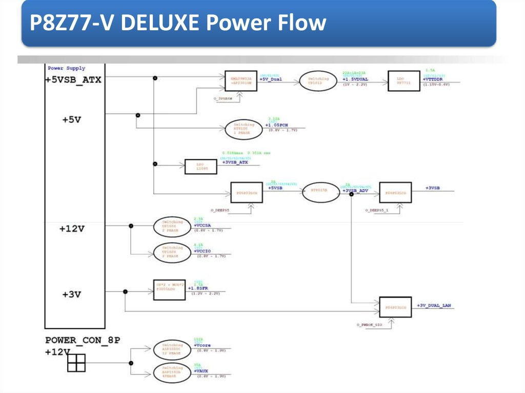
P8Z77-V DELUXE Power Flow11.
Ivy 7 Series – Agenda• Platform Structure
CPU feature introduce
Intel 7 series chipset architecture
Critical Power Flow
Clock Distribution
Power Sequence
Problem Debug
Can’t power on
Power auto shutdown
All dots, zero, and no display
Power part
12.
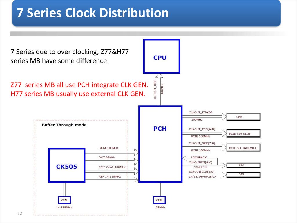
7 Series Clock Distribution7 Series due to over clocking, Z77&H77
series MB have some difference:
Z77 series MB all use PCH integrate CLK GEN.
H77 series MB usually use external CLK GEN.
12
13.
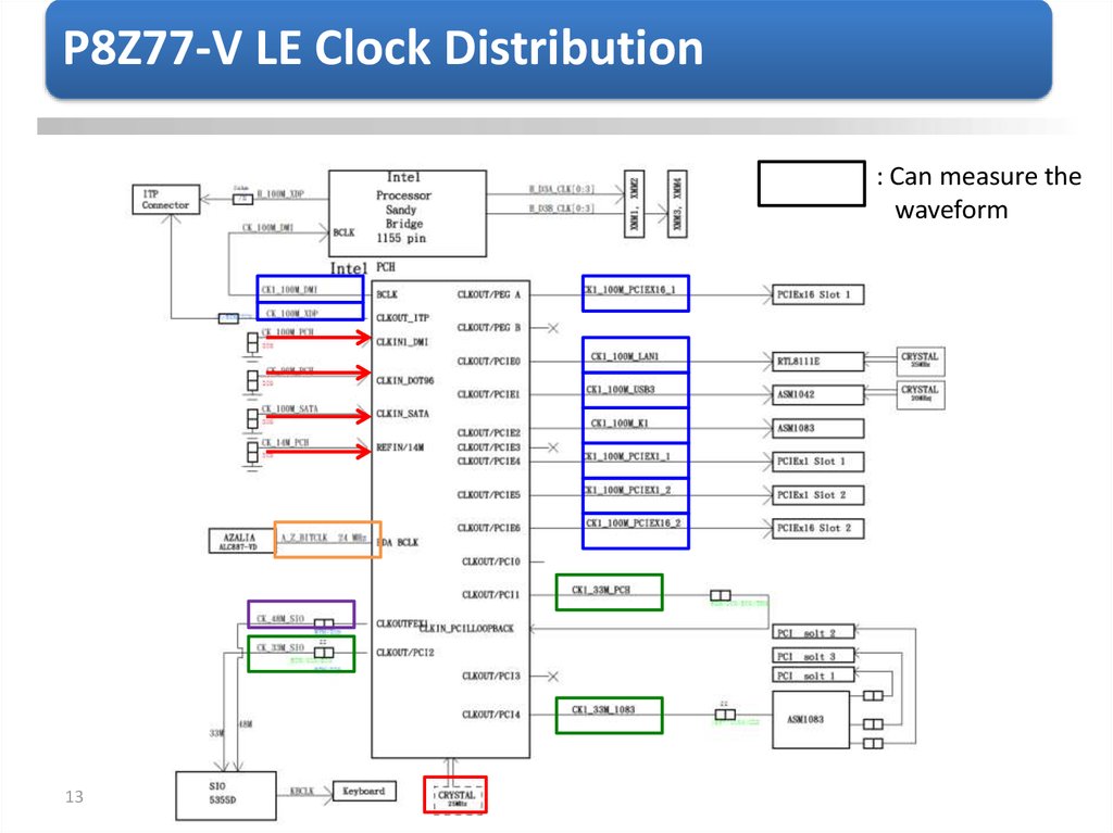
P8Z77-V LE Clock Distribution: Can measure the
waveform
13
14.
SATA clock1. If PCH internal provide CLK, it will use two 10K ohm
resistors to connect to ground.
2. If not, external CLK generator will provide 100M Hz
frequency for PCH
15.
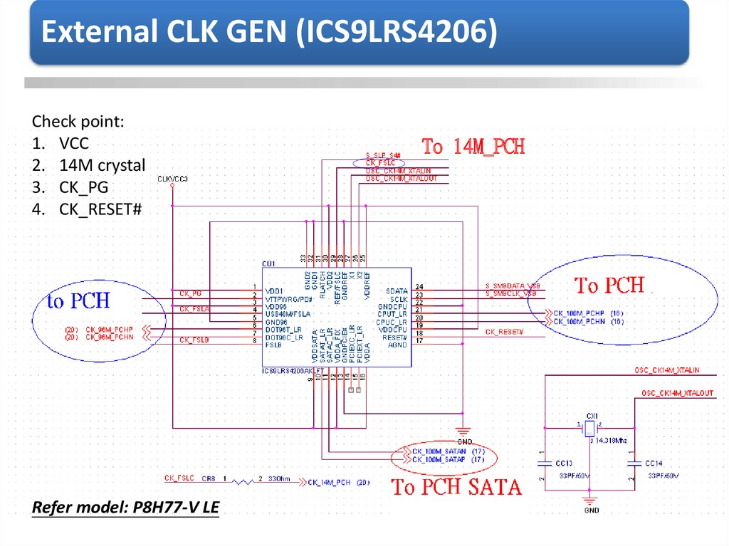
External CLK GEN (ICS9LRS4206)Check point:
1. VCC
2. 14M crystal
3. CK_PG
4. CK_RESET#
Refer model: P8H77-V LE
To 14M_PCH
16.
Ivy 7 Series – Agenda• Platform Structure
CPU feature introduce
Intel 7 series chipset architecture
Critical Power Flow
Clock Distribution
Power Sequence
Problem Debug
Can’t power on
Power auto shutdown
All dots, zero, and no display
Power part
17.
P9X79 DeluxePower
on sequence
- Power Sequence (1)
2
Battery
1
+BAT_3V
3V_ATX
SR107
S_DSWVRMEN
SR106
S_INTVRMEN
SR79
S_SRTCRST#
SR75
S_RTCRST#
3
4
Power
Supply
5
SIO
6
S_RTCRST #
O_RSMRST#
O2_RSMRST#
6
S_RTCRST#
O_RSMRST#
O2_RSMRST#
7
P_+VTTCCIO_REF_10
P_+1.8SFR_REF_10
P_+VCCSA_REF_10
O_PSON#
O2_CUT_PSON#
Refer model: P8Z77-V DELUXE
8
O2_PSON#
18.
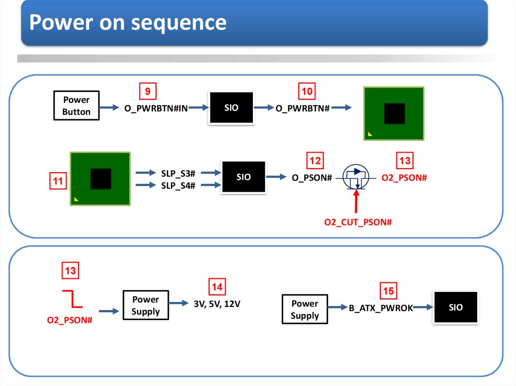
P9X79 DeluxePower
on sequence
- Power Sequence (3)
Power
Button
9
10
SIO
O_PWRBTN#IN
O_PWRBTN#
12
SLP_S3#
SLP_S4#
11
SIO
13
O_PSON#
O2_PSON#
O2_CUT_PSON#
13
14
O2_PSON#
Power
Supply
3V, 5V, 12V
15
Power
Supply
B_ATX_PWROK
SIO
19.
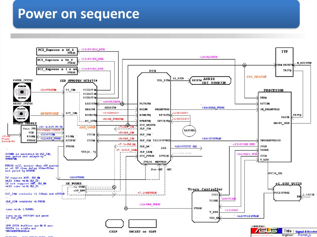
Power on sequence20.
Ivy 7 Series – Agenda• Platform Structure
CPU feature introduce
Intel 7 series chipset architecture
Critical Power Flow
Clock Distribution
Power Sequence
Problem Debug
Can’t power on
Power auto shutdown
All dots, zero, and no display
Power part
21.
Debug - Can’t power on (1)1. Check SIO power sequence and working condition:
+3V_BAT
+3VSB_ATX
+3VSB_ATX
O_IOPWRBTN# (D)
PWRBTN#
PANEL (B)
O_PWRBTN#_R (C)
SLP_S3# (E)
O_RSTCON#
SIO
O_SKTOCC
PCH
SLP_S4# (E)
O_3VSBSW#
RSMRST# (A)
PSON# (F)
ATX_PSON# (G)
22.
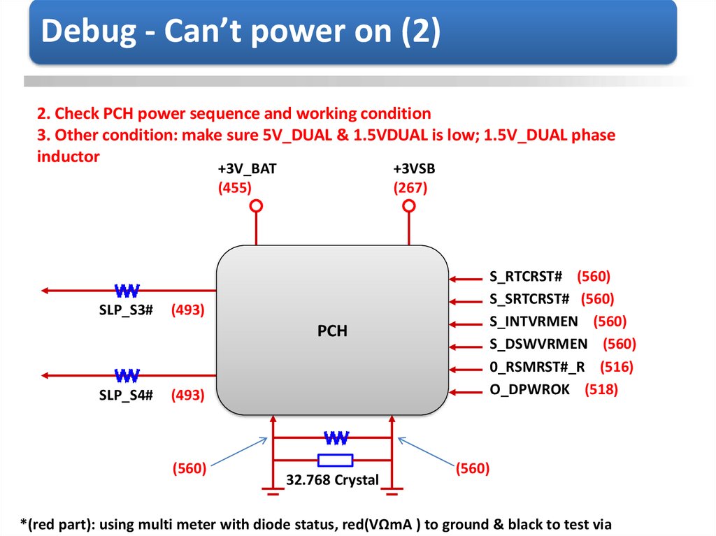
Debug - Can’t power on (2)2. Check PCH power sequence and working condition
3. Other condition: make sure 5V_DUAL & 1.5VDUAL is low; 1.5V_DUAL phase
inductor
+3V_BAT
(455)
SLP_S3#
+3VSB
(267)
S_RTCRST# (560)
S_SRTCRST# (560)
S_INTVRMEN (560)
S_DSWVRMEN (560)
0_RSMRST#_R (516)
O_DPWROK (518)
(493)
PCH
SLP_S4#
(493)
(560)
32.768 Crystal
(560)
*(red part): using multi meter with diode status, red(VΩmA ) to ground & black to test via
23.
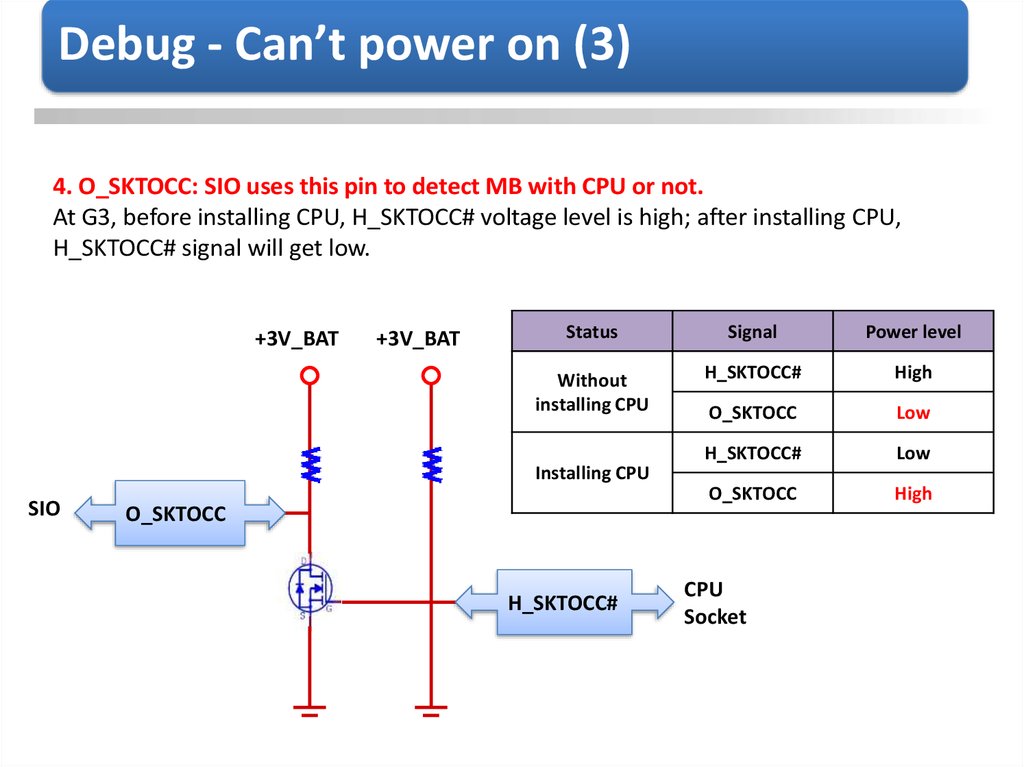
Debug - Can’t power on (3)4. O_SKTOCC: SIO uses this pin to detect MB with CPU or not.
At G3, before installing CPU, H_SKTOCC# voltage level is high; after installing CPU,
H_SKTOCC# signal will get low.
+3V_BAT
+3V_BAT
Status
Signal
Power level
Without
installing CPU
H_SKTOCC#
High
O_SKTOCC
Low
H_SKTOCC#
Low
O_SKTOCC
High
Installing CPU
SIO
O_SKTOCC
H_SKTOCC#
CPU
Socket
24.
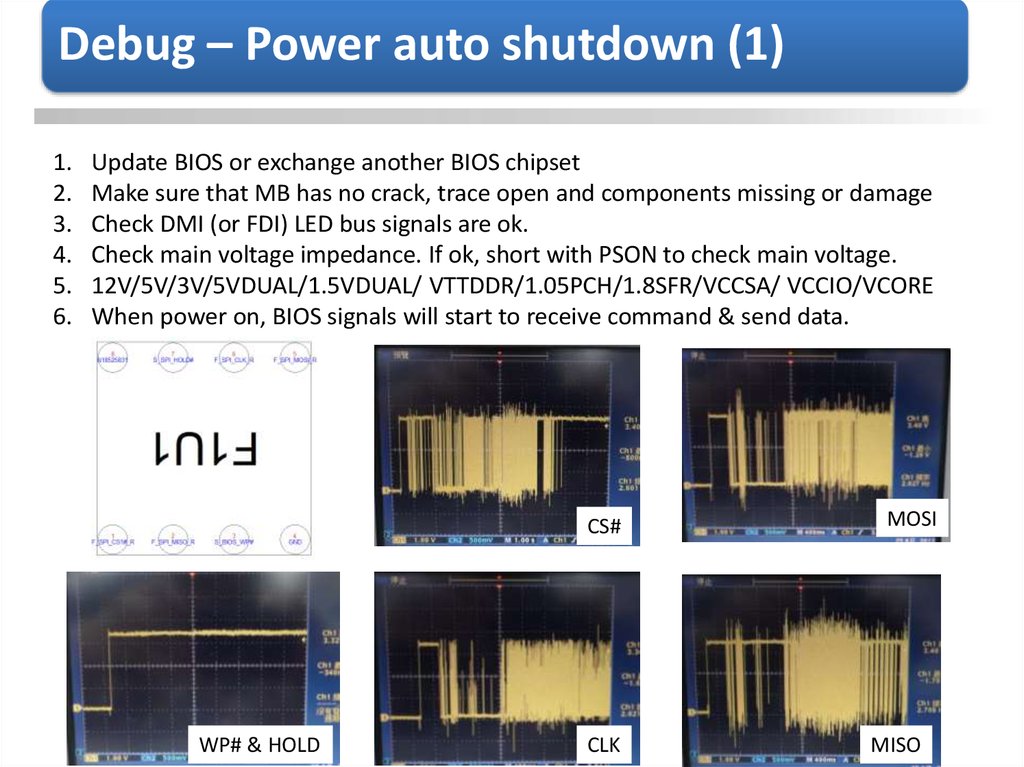
Debug – Power auto shutdown (1)1.
2.
3.
4.
5.
6.
Update BIOS or exchange another BIOS chipset
Make sure that MB has no crack, trace open and components missing or damage
Check DMI (or FDI) LED bus signals are ok.
Check main voltage impedance. If ok, short with PSON to check main voltage.
12V/5V/3V/5VDUAL/1.5VDUAL/ VTTDDR/1.05PCH/1.8SFR/VCCSA/ VCCIO/VCORE
When power on, BIOS signals will start to receive command & send data.
CS#
WP# & HOLD
CLK
MOSI
MISO
25.
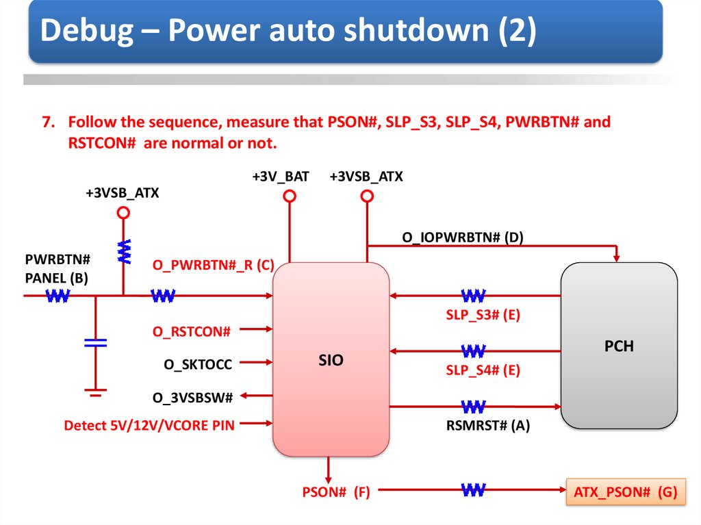
Debug – Power auto shutdown (2)7. Follow the sequence, measure that PSON#, SLP_S3, SLP_S4, PWRBTN# and
RSTCON# are normal or not.
+3V_BAT
+3VSB_ATX
+3VSB_ATX
O_IOPWRBTN# (D)
PWRBTN#
PANEL (B)
O_PWRBTN#_R (C)
SLP_S3# (E)
O_RSTCON#
O_SKTOCC
SIO
PCH
SLP_S4# (E)
O_3VSBSW#
Detect 5V/12V/VCORE PIN
RSMRST# (A)
PSON# (F)
ATX_PSON# (G)
26.
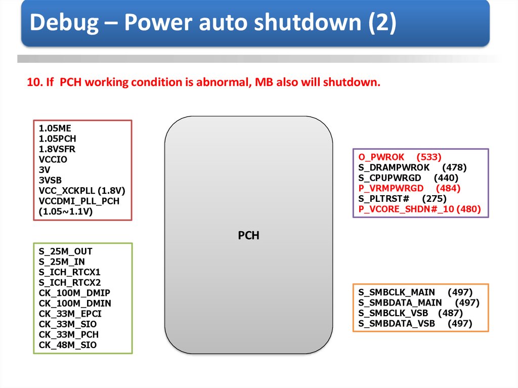
Debug – Power auto shutdown (2)10. If PCH working condition is abnormal, MB also will shutdown.
1.05ME
1.05PCH
1.8VSFR
VCCIO
3V
3VSB
VCC_XCKPLL (1.8V)
VCCDMI_PLL_PCH
(1.05~1.1V)
O_PWROK (533)
S_DRAMPWROK (478)
S_CPUPWRGD (440)
P_VRMPWRGD (484)
S_PLTRST# (275)
P_VCORE_SHDN#_10 (480)
PCH
S_25M_OUT
S_25M_IN
S_ICH_RTCX1
S_ICH_RTCX2
CK_100M_DMIP
CK_100M_DMIN
CK_33M_EPCI
CK_33M_SIO
CK_33M_PCH
CK_48M_SIO
S_SMBCLK_MAIN (497)
S_SMBDATA_MAIN (497)
S_SMBCLK_VSB (487)
S_SMBDATA_VSB (497)
27.
Debug – Power auto shutdown (3)Problem with power shutdown: THERMAL signals, voltage, PCH working condition and
the power sequence (power ok signals)
8. If H_THERMTRIP# is low, P_VCORE_SHDN#_10 will pull low to PCH.
9. If VCORE is abnormal, VRM IC will also use P_VCORE_SHDN#_10 to pull low.
VCCIO
+3V
P_VCORE_SHDN#_10
VRM
IC
PCH
CPU
H_THERMTRIP#
28.
Debug – All dots, zero, and no displayBefore 00:
1. Power on
2. Power/CLK/RST
3. CPURST#
DMI
FDI
After 00 and CPURST#:
1. CPU to PCH (DMI)
2. PCH to BIOS (SPI)
3. SPI to PCH (SPI)
4. PCH to CPU (DMI)
PCH to MEMORY (SMB)
5. CPU to MEMORY
6. PCH to SIO (LPC)
PCH to EC
7. PCH to DEVICE
8. CPU to PCH (FDI)
9. PCH to DVI/VGA/HDMI
CPU to PCIEX16
CPU
PCIEX16
SMB
DVI
SATA
VGA
USB
HDMI
LAN
USB
3.0
Audio
SPI
LPC
SIO
O2_SMB
29.
Debug – All dots, zero, and no displayMeasure BUS:
1. DMI:
H_DMI_RXN/P[0:3]
H_DMI_TXN/P[0:3]
S_DMICOMP
S_DMIRBIAS
VCCDMI_PLL_PCH
2. FDI:
H_FDI_INT
H_FDI_COMP
H_FDI_FSYNC[0:1]
H_FDI_LSYNC[0:1]
H_FDI_TXN/P[0:7]
D3A_CLKP/N[0:1]
D3A_CS#[0:1]
D3A_ODT[0:1]
D3A_CKE[0:1]
D3A_WE#
D3A_RAS#
D3A_CAS#
DMI
4. Memory to CPU
D3A_DQ[0:63]
D3A_MA[0:15]
D3A_DQSN/P[0:7]
D3A_BA[0:2]
D3_RESET#
FDI
3. SMB:
S_SMBCLK_MAIN
S_SMBDATA_MAIN
S_SMBCLK_PCI
S_SMBDATA_PCI
CPU
SMB
30.
Debug – All dots, zero, and no displayChipset (EC C.SEPT036)
F_FRAME#
F_SERIRQ#
F_LAD [0:3]
C_PCI_EC
S_PLTRST
O2_VREF
3VSB
O2_VDDA (O2_3.2V)
LPC
ADC
SMBUS
FAN
O2_SMB1_CLK/DATA
O2_SMB2_CLK/DATA
24M Crystal
CLOCK
O2_PWM1 (VCCSA)
O2_PWM2 (VCCIO)
O2_PWM3 (1.8SFR)
PWM
Refer model: P8Z77-V DELUXE
EC
C.SEPT036
O2_AD0
O2_AD1
O2_AD2
O2_AD3
(1.05PCH)
(VCCIO)
(1.8SFR)
(1.5DUAL)
O2_SEN_CPUOPT
O2_OP_MODE
OP_MODE
Control
O2_RSMRST#
O2_CUT_PSON#
O2_VAUX_OUT
O_PWRBTN#IN_R
O2_RSTCON#_R
O2_VRMPWRGD
VRMPWRGD
S_SLPS3#/S4#
O_PWROK
J_SILENT#
31.
Debug – All dots, zero, and no displayChipset (EC C.SKB3722)
Intel input voltage
Output
voltage
Refer model: P8Z77-V LE
32.
Debug – All dots, zero, and no displayChipset (EC C.SKB3722)
EC of S3, S4 signals
will change with
different status.
Before boot up, EC will
install LPC signal and
sent ECPG for PWROK.
After boot up, BIOS
will through LPC to
let EC over voltage
Refer model: P8Z77-V LE
33.
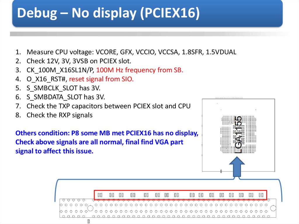
Debug – No display (PCIEX16)1.
2.
3.
4.
5.
6.
7.
8.
Measure CPU voltage: VCORE, GFX, VCCIO, VCCSA, 1.8SFR, 1.5VDUAL
Check 12V, 3V, 3VSB on PCIEX slot.
CK_100M_X16SL1N/P, 100M Hz frequency from SB.
O_X16_RST#, reset signal from SIO.
S_SMBCLK_SLOT has 3V.
S_SMBDATA_SLOT has 3V.
Check the TXP capacitors between PCIEX slot and CPU
Check the RXP signals
Others condition: P8 some MB met PCIEX16 has no display,
Check above signals are all normal, final find VGA part
signal to affect this issue.
34.
Debug – No display (VGA)1. FDI and DMI Bus, make sure that all LED lights are normal
2. CPU voltage: VCORE, GFX, VCCIO, VCCSA, 1.8SFR, 1.5VDUAL
3. P_GFX_OK_10, when debug code run to b2, P_GFX_OK_10 will pull high to 3V, at
the same time, GFX power will drop from 1V to 0.4~0.5V
4. +5V_D_VGA has 5V
5. Check the RGB GND impedance (77 ohm)
6. Check S_VGA_VSYNC and S_VGA_HYSNC GND impedance (500 ohm)
7. Check VGA_DDC_CLK and VGA_DDC_DATA impedance (538 ohm)
8. Check PCH V_3P3_DAC_FB (3V)
9. S_DAC_IREF(0.6), after b2 code, this signal’s power level will raise up
10. 25M Hz crystal
11. Other device also will affect this problem
EX: P8P67 LE halt at b2
Exchange USB3.0 IC (ASM1042)
To solve this case
35.
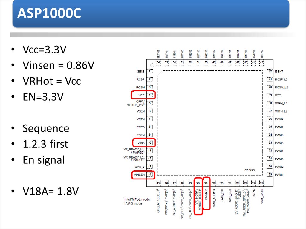
ASP1000CVcc=3.3V
Vinsen = 0.86V
VRHot = Vcc
EN=3.3V
• Sequence
• 1.2.3 first
• En signal
• V18A= 1.8V
36.
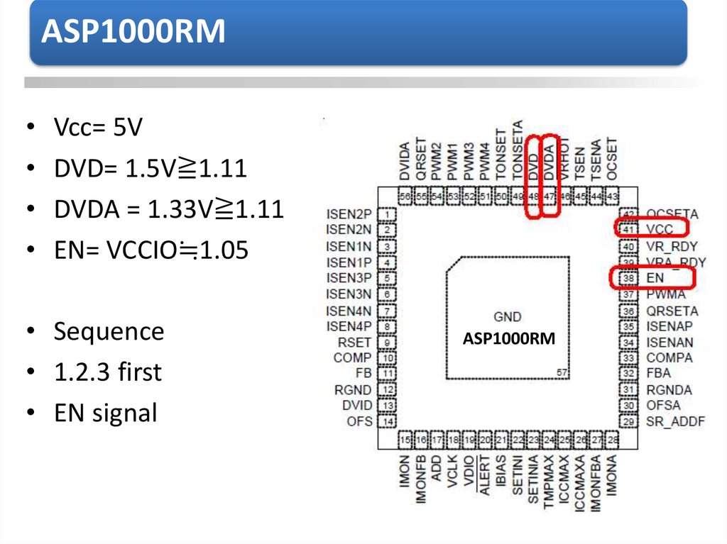
ASP1000RMVcc= 5V
DVD= 1.5V≧1.11
DVDA = 1.33V≧1.11
EN= VCCIO≒1.05
• Sequence
• 1.2.3 first
• EN signal
ASP1000RM
37.
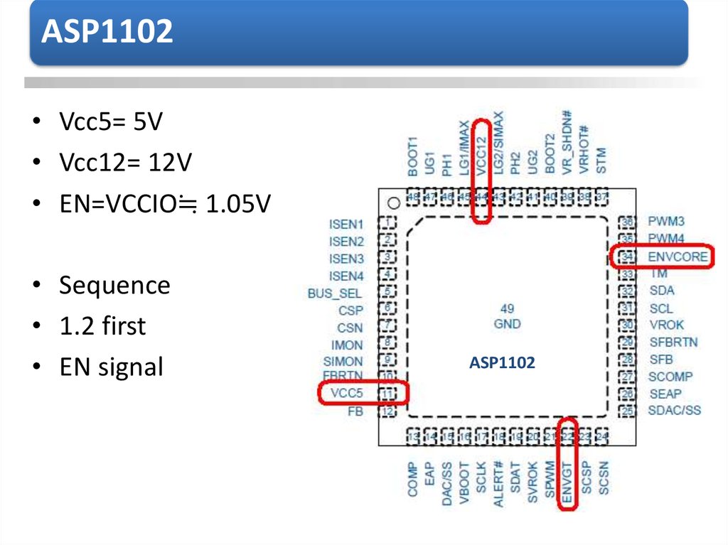
ASP1102• Vcc5= 5V
• Vcc12= 12V
• EN=VCCIO≒ 1.05V
• Sequence
• 1.2 first
• EN signal
ASP1102
38.
VCORE Driver (ASP0A13)ASP0A13
39.
VCORE Driver (ASP0A13)RT9611
IR8510
40.
Debug - Vcore RepairingVcore voltage output of each phase must have the correct waveform
Empty board boot to Vcore is about 1V boot voltage .
After installing CPU, it is set with the SVID voltage, so the value is different.
VCORE run normally, but still halts at 00=>check PG signals.
41.
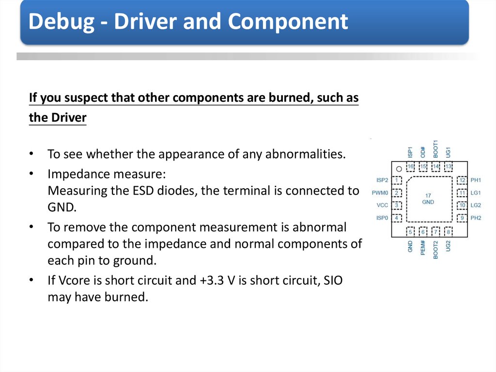
Debug - Driver and ComponentIf you suspect that other components are burned, such as
the Driver
• To see whether the appearance of any abnormalities.
• Impedance measure:
Measuring the ESD diodes, the terminal is connected to
GND.
• To remove the component measurement is abnormal
compared to the impedance and normal components of
each pin to ground.
• If Vcore is short circuit and +3.3 V is short circuit, SIO
may have burned.
42.
Debug – 5VSB1. Clear COMS and let MB at load default status
2. Check +5VSB_ATX
3. Check O_DEEPS5 and PQ305
high
low
low
43.
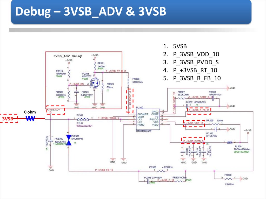
Debug – 3VSB_ADV & 3VSB1.
2.
3.
4.
5.
0 ohm
3VSB
5VSB
P_3VSB_VDD_10
P_3VSB_PVDD_S
P_+3VSB_RT_10
P_3VSB_R_FB_10
44.
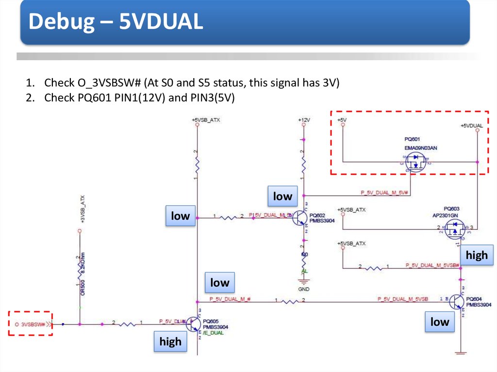
Debug – 5VDUAL1. Check O_3VSBSW# (At S0 and S5 status, this signal has 3V)
2. Check PQ601 PIN1(12V) and PIN3(5V)
low
low
high
low
low
high
45.
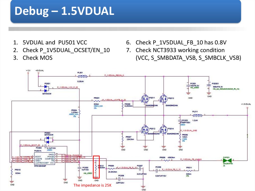
Debug – 1.5VDUAL1. 5VDUAL and PU501 VCC
2. Check P_1V5DUAL_OCSET/EN_10
3. Check MOS
The impedance is 25K
6. Check P_1V5DUAL_FB_10 has 0.8V
7. Check NCT3933 working condition
(VCC, S_SMBDATA_VSB, S_SMBCLK_VSB)
46.
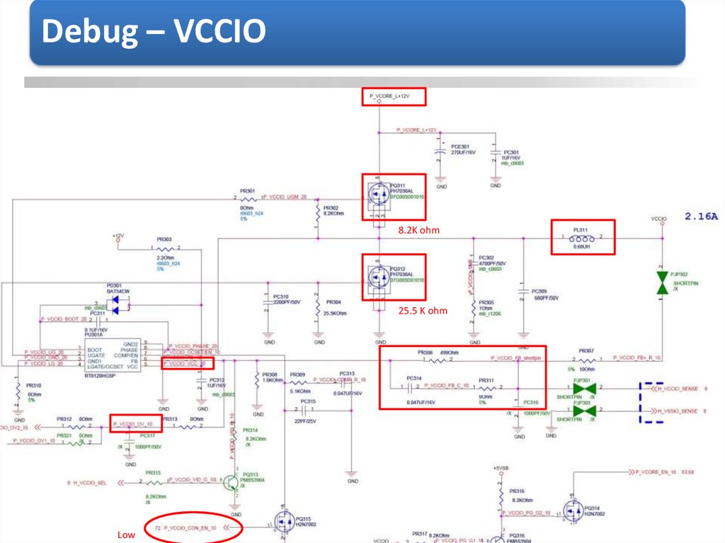
Debug – VCCIO8.2K ohm
25.5 K ohm
Low
47.
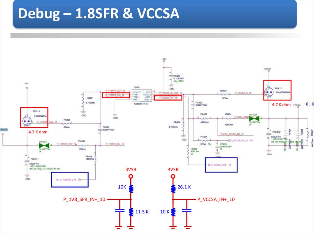
Debug – 1.8SFR & VCCSA4.7 K ohm
4.7 K ohm
3VSB
3VSB
10K
26.1 K
P_1V8_SFR_IN+_10
P_VCCSA_IN+_10
11.5 K
10 K
48.
Q&AThank You!