


 Информатика
Похожие презентации:


")


Unit 2. Computer System’s Silicon miracles: How GPUs are made
1.
Unit 2 Computer System’sSilicon Miracles: How GPUs are made
Free Powerpoint Templates
2.
Aims & Objectives:• This lesson describes how using
some of the most advanced and
intricate engineering modes and
mechanisms
• Silison can be transformed into
some of the most Powerful
General/Graphical Processing
units we have ever seen
Free Powerpoint Templates
Page 2
3.
Sand to Silicon:• Silicon is one of the few chemical
elements known as aa Matalloid
• This means it has the neccessary
properties to form semiconductors
• These semiconductors are the basis
of all digital electronics
• For silicon production ‘Silica’ sand is
required, this sand is made of
mainly silicon dioxide
• Silica sand is heated to 2000
degrees centigrade in the presence
Powerpoint Templates
of Free
carbon
Page 3
4.
Sand to Silicon:• The carbon reacts with the oxygen
in the silica to produce elemental
silicon
• The metallurgical grade silicon is
99% pure
• For th GPU this silicon needs to
further purified (1 in 1,000,000
pure)
• Purification is achieved by reacting
silicon with hydrogen chloride
• The silicon compound is extracted
by fractional distilation and reintorduced to hydrogen
Free Powerpoint Templates
Page 4
5.
From silicon to wafers…Silicon wafers are usually 300mm in diameter
and 0/775mm thick
Rather than being composed of lots of small
crystals that would have a negative impact on
the silicons electronic properties and to avoid
defects silicon must be grown as a single
crystal
Pure silicon is melted at just above its melting
point of 1,414 degree’s centigrade
A tiny crystal of silicon is dipped into the
molton silicon and slowly withdrawn
(millimeters per hour)
A monocrystaline rod, called a boule is
produced
It is sliced up using a wire saw
The wafers are then ground and polished so
that they are flat within two thousandths of a
Free Powerpoint Templates
millimeter
Page 5
6.
The General / GraphicalProcessing Unit:
• Engineers have now managed to design
and build machines with components
measuing as little as 40nm across…
• A Nanometer measure one-thousandth
the diameter of a human hair
• A powerful Intel i7 sandbridge CPU
boasts just short of one billion
transistors
• A leading edge general processing
unit like AMDs Cayman, used in the
Radeon HD 6970 graphics card clocks up
a massive 2.64 billion transistors
Free Powerpoint Templates
Page 6
7.
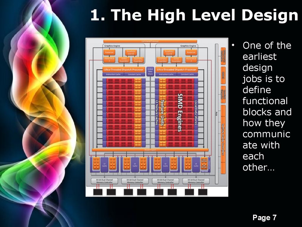
1. The High Level Design• One of the
earliest
design
jobs is to
define
functional
blocks and
how they
communic
ate with
each
other…
Free Powerpoint Templates
Page 7
8.
2. Floorplan and Netlist• The floorplan must now be defined
• This is a physical representation that will take account of
how large each block is expected to be and where it
should be positioned relative to other blocks
• Account is taken of how many signals pass between the
blocks with the aim of reducing the lengths of the
pathways
• OtherFree
engineers
work Templates
on the component level design of
Powerpoint
Page 8
each of the blocks.
9.
3. Circuit verificationand emulation
• Designs as complicated as a GPU are never
100 per cent correct on the first attempt
• So the design is verified and emulated - a
hugely processor-intensive operation that
requires supercomputing resources
• Verification involves testing individual blocks
with perhaps thousands of tests per block
• Each time anything fails, the design team
backtracks to correct the errors and then
performs a full set of simulation tests to make
sure the remedial action hadn't broken
something that previously worked correctly
Free Powerpoint Templates
Page 9
10.
3. Circuit verificationand emulation
• Once all the individual blocks are operational,
the team moves to emulation
• This means exercising the GPU as a whole,
but given the amount of processing time
needed to simulate a multi-billion transistor
chip, these tests might initially be nothing
more complicated than drawing a single pixel
• In addition to functional testing, emulation also
ensures that the chip meets its requirements
in terms of processing speed.
Free Powerpoint Templates
Page 10
11.
4. Making the masks• With the simulation out of the way the
designers know that the circuit connections
are correct
• However, no thought has been given to where
the components go on the chip
• This is carried out using a special CAD
package, driven by the floor-plan
• This largely automated process places each
component and routes the copper tracks that
will ultimately connect them all together
• The culmination of this process is a major
milestone referred to as 'tape out', and marks
the transition from design to fabrication
Free Powerpoint Templates
Page 11
12.
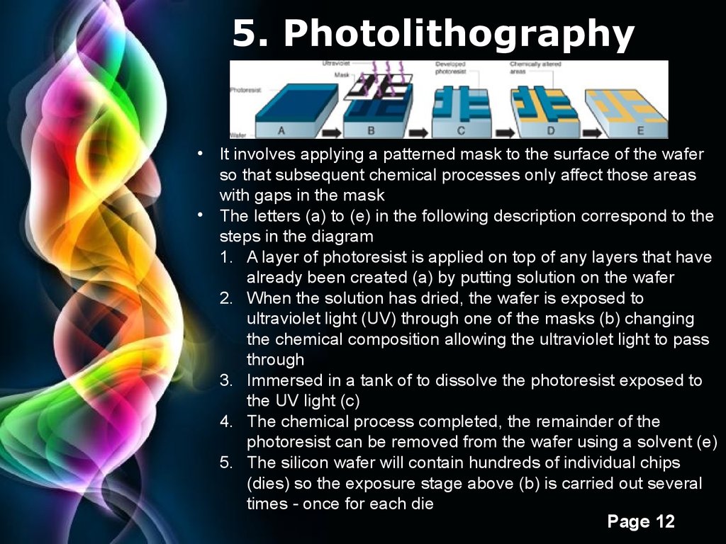
5. Photolithography• It involves applying a patterned mask to the surface of the wafer
so that subsequent chemical processes only affect those areas
with gaps in the mask
• The letters (a) to (e) in the following description correspond to the
steps in the diagram
1. A layer of photoresist is applied on top of any layers that have
already been created (a) by putting solution on the wafer
2. When the solution has dried, the wafer is exposed to
ultraviolet light (UV) through one of the masks (b) changing
the chemical composition allowing the ultraviolet light to pass
through
3. Immersed in a tank of to dissolve the photoresist exposed to
the UV light (c)
4. The chemical process completed, the remainder of the
photoresist can be removed from the wafer using a solvent (e)
5. The silicon wafer will contain hundreds of individual chips
(dies) so the exposure stage above (b) is carried out several
times
- once
for each die
Free
Powerpoint
Templates
Page 12
13.
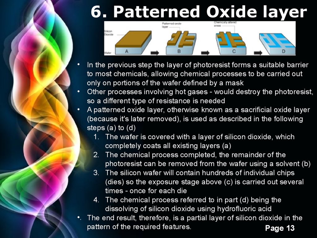
6. Patterned Oxide layer• In the previous step the layer of photoresist forms a suitable barrier
to most chemicals, allowing chemical processes to be carried out
only on portions of the wafer defined by a mask
• Other processes involving hot gases - would destroy the photoresist,
so a different type of resistance is needed
• A patterned oxide layer, otherwise known as a sacrificial oxide layer
(because it's later removed), is used as described in the following
steps (a) to (d)
1. The wafer is covered with a layer of silicon dioxide, which
completely coats all existing layers (a)
2. The chemical process completed, the remainder of the
photoresist can be removed from the wafer using a solvent (b)
3. The silicon wafer will contain hundreds of individual chips
(dies) so the exposure stage above (c) is carried out several
times - once for each die
4. The chemical process referred to in part (d) being the
dissolving of silicon dioxide using hydrofluoric acid
•. The end result, therefore, is a partial layer of silicon dioxide in the
Powerpoint
Templates
pattern of Free
the required
features.
Page 13
14.
7. Creating the transistors• A MOSFET (the type of transistor used in
GPUs) is an electronic switch
• It is an electronic component that uses a
signal on one circuit to control the flow of
current in another
• This is the most fundamental requirement in
digital electronics
• Here we see how an n-channel MOSFET is
created, but p-channel MOSFETs are also
required.
• They differ only in that one has n-type
material
where theTemplates
other has p-type, and vice
Free Powerpoint
Page 14
versa
15.
7. Creating the Transistors• In the following description, changes are
made selectively to parts of the wafer by use
of either a layer of photoresist or a patterned
oxide layer
• The wafer is bombarded with phosphorous
ions that implant themselves into the silicon
through the gaps in the photoresist to create
so-called wells of n-type material
• This is a modified form of silicon that has
additional electrodes to carry an electrical
current
Free Powerpoint Templates
Page 15
16.
7. Creating the Transistors• Two smaller islands of p-type material are
created within the n-type wells
• These form the two electrodes known as the
source and the drain of the MOSFETs
• Then, a very thin insulating layer of silicon
dioxide, just a few molecules thick, is
deposited on the surface of the silicon
between the source and the drain
• This is done in a furnace filled with gases to
chemically modify the silicon
• Finally, a layer of silicon is applied over the
oxide layer to create the MOSFETs' third and
final electrode, which is called the gate
Free Powerpoint Templates
Page 16
17.
8. Connecting Everything• We now have a wafer comprising several dies,
each of which contains billions of transistors, but
to convert these from isolated components into
a working circuit they have to be connected
using copper tracks
• First, an insulating layer of silicon dioxide is
applied to the wafer so that the interconnecting
tracks don't short all the MOSFETs together
• Next, holes are etched in the silicon dioxide so
that connections can be made to the MOSFETs'
electrodes
• Then, trenches in the shape of the tracks are
etched into the silicon dioxide before a layer of
copper is applied by electro-plating
Free Powerpoint Templates
Page 17
18.
8. Connecting Everything• This covers the entire surface of the silicon dioxide, and
fills the trenches and the holes to make contact with the
MOSFETs.
• Finally, the excess copper is removed using a process
called chemical-mechanical polishing so that copper
only remains in the trenches and holes
• A single layer of copper interconnections isn't enough to
create a viable circuit
• it isn't possible to connect everything in a single layer
without making shorts, additional layers are used, each
created in the same way as the first copper layer
• Increasing the number of layers can reduce the size of
the chip, and some layers have to be dedicated to
providing power, so ten or more layers isn't unusual in
top-end chips.
Free Powerpoint Templates
Page 18
19.
9. Testing• The initial manufacturing processes are now
complete to the extent that the wafer will
contain several hundred dies
• next is to test the dies one at a time, this is
carried out using a sophisticated piece of
equipment called a wafer prober, which
makes electrical contact with microscopic
pads on the dies
• In this fully automated process, the machine
remembers which of the dies passed the
test
• Typically, for a state-of-the-art chip, the yield
is in the 50-60% area
Free Powerpoint Templates
Page 19
20.
10. PackagingOnce testing is complete, the wafer is sawn up into
individual dies and the non-functional ones are
discarded
The final step is to take the working dies - tiny
rectangles of silicon that are far too flimsy to be used
as regular electronic components - and package
them into what most people think of as a chip, ready
to be soldered onto a circuit board
This involves bonding the die onto a substrate, and
making connections between the minuscule pads on
the die and the somewhat larger solder bumps that
will eventually be used to make the electrical
connections on a graphics card
A final functional test is carried out to ensure that the
packing has been successful, and this miracle of
digital technology is then ready to be shipped to the
Free Powerpoint Templates
graphics
card manufacturing facility
Page 20